EP1599068A1 - Thermally excited sound wave generating device - Google Patents
Thermally excited sound wave generating device Download PDFInfo
- Publication number
- EP1599068A1 EP1599068A1 EP04715490A EP04715490A EP1599068A1 EP 1599068 A1 EP1599068 A1 EP 1599068A1 EP 04715490 A EP04715490 A EP 04715490A EP 04715490 A EP04715490 A EP 04715490A EP 1599068 A1 EP1599068 A1 EP 1599068A1
- Authority
- EP
- European Patent Office
- Prior art keywords
- generating device
- sound wave
- wave generating
- insulation layer
- heat
- Prior art date
- Legal status (The legal status is an assumption and is not a legal conclusion. Google has not performed a legal analysis and makes no representation as to the accuracy of the status listed.)
- Withdrawn
Links
Images


Classifications
-
- H—ELECTRICITY
- H04—ELECTRIC COMMUNICATION TECHNIQUE
- H04R—LOUDSPEAKERS, MICROPHONES, GRAMOPHONE PICK-UPS OR LIKE ACOUSTIC ELECTROMECHANICAL TRANSDUCERS; DEAF-AID SETS; PUBLIC ADDRESS SYSTEMS
- H04R23/00—Transducers other than those covered by groups H04R9/00 - H04R21/00
- H04R23/002—Transducers other than those covered by groups H04R9/00 - H04R21/00 using electrothermic-effect transducer
-
- B—PERFORMING OPERATIONS; TRANSPORTING
- B06—GENERATING OR TRANSMITTING MECHANICAL VIBRATIONS IN GENERAL
- B06B—METHODS OR APPARATUS FOR GENERATING OR TRANSMITTING MECHANICAL VIBRATIONS OF INFRASONIC, SONIC, OR ULTRASONIC FREQUENCY, e.g. FOR PERFORMING MECHANICAL WORK IN GENERAL
- B06B1/00—Methods or apparatus for generating mechanical vibrations of infrasonic, sonic, or ultrasonic frequency
- B06B1/02—Methods or apparatus for generating mechanical vibrations of infrasonic, sonic, or ultrasonic frequency making use of electrical energy
-
- G—PHYSICS
- G10—MUSICAL INSTRUMENTS; ACOUSTICS
- G10K—SOUND-PRODUCING DEVICES; METHODS OR DEVICES FOR PROTECTING AGAINST, OR FOR DAMPING, NOISE OR OTHER ACOUSTIC WAVES IN GENERAL; ACOUSTICS NOT OTHERWISE PROVIDED FOR
- G10K15/00—Acoustics not otherwise provided for
- G10K15/04—Sound-producing devices
Definitions
- the invention of this application relates to a thermally induced sound wave generating device. More specifically, the invention of this application relates to a new thermally induced sound wave generating device that creates compressional wave of the air by giving heat to the air to generate sound waves and is useful for an ultrasonic sound source, a speaker sound source, an actuator, and the like.
- ultrasonic wave generating devices have been known. All of these conventional ultrasonic wave generating devices convert some mechanical vibration into vibration of the air except special ones that use electric spark, fluid vibration, and the like.
- a method of using such mechanical vibration although there are a moving conductor type, a capacitor type, and the like, a method utilizing a piezoelectric element is mainly used in an ultrasonic region.
- electrodes are formed on both surfaces of barium titanate serving as a piezoelectric material and an ultrasonic electric signal is applied between the electrodes, whereby mechanical vibration is generated and the vibration is transmitted to a medium such as the air to generate ultrasonic waves.
- the pressure wave generating device includes a substrate, a heat insulation layer provided on the substrate, and a heating element thin film that is provided on the heat insulation layer and driven electrically.
- the heat insulation layer such as a porous layer or a polymeric layer having extremely small thermal conductivity for heat generated from the heating element thin film, a temperature change in an air layer on the surface of a heating element is increased to generate ultrasonic sounds.
- the device Since the proposed device does not involve mechanical vibration, the device has characteristics that a frequency band is wide, the device is less susceptible to influences of an ambient environment, and it is relatively easy to fine and array the device.
- a change in surface temperature at the time when an AC current is applied to the electrically-driven heating element thin film is given by the following expression (1) when thermal conductivity of the heat insulation layer is set as ⁇ , a heat capacity per volume thereof is set as C, and an angular frequency thereof is set as ⁇ , and there is output and input of energy per a unit area of q( ⁇ )[W/cm 2 ].
- T( ⁇ ) (1-j)/ 2 ⁇ 1/ ⁇ C ⁇ q( ⁇ )
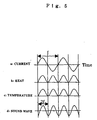
- a temperature change of the air is caused (Fig. 5-c) by heat exchange of heat (Fig. 5-b), which is generated from the heating element thin film by an electric current (Fig. 5-a) with a frequency f supplied from a signal source for generating a signal of an ultrasonic frequency, with the air that is a medium around the heating element thin film.
- a frequency f supplied from a signal source for generating a signal of an ultrasonic frequency
- the sound pressure to be generated is larger as the thermal conductivity ⁇ and the heat capacity per volume C of the thermal insulation layer are smaller, and is proportional to the output and input q( ⁇ ) of energy per a unit area, that is, input electric power.
- thermal contrast of the heat insulation layer and the substrate plays an important role.
- the sound wave generating device based on thermal induction, under the present situation, no actual prospects are opened up from the viewpoint of improvement in performance thereof concerning an issue of how a multilayer structure thereof should be and concerning a specific form thereof.
- the sound wave generating device does not involve mechanical vibration at all and has many characteristics, there is a problem in that, when it is attempted to obtain practical output, Joule heat generated by an increase in input power also increases due to increase of input power, it is impossible to permit heat of a DC component to escape completely, and it is impossible to increase a temperature change in the heating element thin film.
- a level of a sound pressure to be generated is about 0.1 Pa at the maximum, which is not a satisfactory level. Therefore, further improvement in the performance has been desired.
- the invention of this application provides, as a device for solving the problems, a thermally induced sound wave generating device including: a thermally conductive substrate; a heat insulation layer formed on one surface of the substrate; and a heating element thin film formed on the heat insulation layer and in the form of an electrically driven metal film, and wherein when thermal conductivity of the thermally conductive substrate is set as ⁇ S and a heat capacity thereof is set as C S , and thermal conductivity of the heat insulation layer is set as ⁇ I , and its capacity is set as C I , relation of 1/100 ⁇ I C I / ⁇ S C S and ⁇ S C S ⁇ 100 ⁇ 10 6 is realized.
- the invention provides the thermally induced sound wave generating device that is characterized in that the thermally conductive substrate consists of a semiconductor or metal.
- the invention provides the thermally induced sound wave generating device that is characterized in that the thermally conductive substrate consists of a ceramics substrate.
- the inventors repeated studies earnestly paying attention to thermal contrast of the heat insulation layer and the substrate in order to solve the problems and, as a result of the studies, the invention of this application is derived.
- the invention is completed on the basis of a totally unexpected new knowledge that performance is improved by selecting materials for the thermally conductive substrate and the heat insulation layer such that the relation described above is realized.
- the invention of this application provides the thermally induced sound wave generating device that is characterized in that the heat insulation layer is a porous silicon layer that is formed on one surface of the thermally conductive substrate by anodizing polycrystalline silicon.
- the invention provides the thermally induced sound wave generating device that is characterized in that the porous silicon layer has silicon grains of a columnar structure at least in a part in the porous silicon layer.
- the invention is derived from the result of the earnest studies by the inventors and is completed on the basis of a totally unexpected new knowledge that, by using the porous silicon layer, which is formed by making polycrystalline silicon porous, as the heat insulation layer, a part of the porous silicon layer plays a role of permitting heat of a DC component to escape to the substrate side efficiently.
- the invention of this application provides the thermally induced sound wave generating device that is characterized in that, in the porous silicon layer, dielectric films are formed on surfaces of nanocrystalline silicon.
- the invention provides the thermally induced sound wave generating device, characterized in that the dielectric films are oxide films.
- the invention provides the thermally induced sound wave generating device that is characterized in that the dielectric films are nitride films.
- the invention provides the thermally induced sound wave generating device that is characterized in that the dielectric films are formed according to heat treatment.
- the invention provides the thermally induced sound wave generating device that is characterized in that the dielectric films are formed according to electrochemical treatment.
- a thermally induced sound generating device that is characterized by including: a thermally conductive substrate; a heat insulation layer consisting of a porous silicon layer that is formed on one surface on the substrate; and a heating element thin film consisting of a metal film that is formed on the heat insulation layer and driven electrically, it is possible to decrease thermal conductivity ⁇ in a heat insulation layer and it is possible to increase a generated sound pressure by forming dielectric films on surfaces of nanocrystalline silicon of the porous silicon layer.
- Fig. 1 is a sectional view illustrating an embodiment mode of a thermally induced sound wave generating device according to the invention of this application.
- the thermally induced sound wave generating device includes: a thermally conductive substrate (1), a heat insulation layer (2) consisting of a porous silicon layer that is formed on one surface of the substrate, and a heating element thin film (3) consisting of a metal film that is formed on the heat insulation layer (2) and driven electrically.
- a thickness of a thermally insulating layer having thermal conductivity a and a heat capacity per volume C is set to L and there is a thermally conductive substrate having sufficiently large ⁇ and C below the thermally insulating layer, if the heat insulation layer has a thickness (a thermal diffusion length) of a degree represented by the expression (3), it is possible to insulate an AC component of generated heat and permit heat of a DC component, which is generated because of a heat capacity of a heating element, to escape to the substrate having large thermal conductivity.
- materials for the heat insulation layer and the substrate are selected and combined such that ⁇ I C I is within a range of 1/100 ⁇ I C I / ⁇ S C S and ⁇ S C S ⁇ 100 ⁇ 10 6 .
- ⁇ I C I is within a range of 1/100 ⁇ I C I / ⁇ S C S and ⁇ S C S ⁇ 100 ⁇ 10 6 .
- ⁇ C of a solid body generally takes values in ranges indicated in Table 1 in cases of metal, a semiconductor, an inorganic insulator, and resin.
- the porous silicon is a porous body of silicon that can be formed by, for example, subjecting a silicon surface to anodic oxidation treatment in a hydrogen fluoride solution. It is possible to obtain a desired porosity and a desired depth (thickness) by appropriately setting an electric current density and treatment time.
- the porous silicon is a porous material and shows extremely small values in both thermal conductivity and a heat capacity compared with silicon according to a quantum effect (a phonon confinement effect) of nano-sized silicon.
- the polyimide, the porous silicon, the polystyrene foam, and the like can be used as the heat insulation layer.
- the combination of these heat insulating materials is only an example and a combination of heat insulating materials can be selected appropriately.
- heat insulating materials, from which the heat insulation layers can be manufactured in an easy manufacturing process such as fining/arraying treatment, are selected.
- the heat insulation layer (2) consisting of the porous silicon layer by subjecting the silicon surface to the anodic oxidation treatment in a hydrogen fluoride solution.
- a desired porosity and a desired depth (thickness) by appropriately setting an electric current density and treatment time.
- the porous silicon is a porous material and shows extremely small values in both thermal conductivity and a heat capacity compared with silicon according to a quantum effect (a phonon confinement effect) of nano-sized silicon.
- the porous silicon with a porosity of about 70% has the thermal conductivity ⁇ of 0.12 W/mK and the heat capacity C of 0.06 ⁇ 10 6 J/m 3 K.
- the silicon it is possible to use polycrystalline silicon rather than single crystalline silicon.
- the polycrystalline silicon can be formed by, for example, the plasma CVD method. However, a method of formation is not specifically limited.
- the polycrystalline silicon may be formed according to the catalyst CVD method or may be obtained by forming a film of amorphous silicon according to the plasma CVD method and, then, applying laser anneal to the amorphous silicon film as heating treatment to thereby polycrystallize the amorphous silicon film.
- the polycrystalline silicon is treated according to the anodic oxidation method, as shown in Fig.
- thermal conductivity of SiO 2 and Si 3 N 4 which were insulating materials, was small compared with thermal conductivity of the silicon that was a skeleton of the porous silicon.
- the inventors found that it was possible to reduce the thermal conductivity ⁇ of the porous silicon by forming dielectric films on surfaces of nanocrystalline silicon forming the porous silicon and decreasing thermal conductivity of the skeleton portions.
- heat capacities C of these insulating materials is large compared with that of the silicon, it is necessary to appropriately select a thickness of the dielectric films to be formed on the surfaces of the silicon crystals such that the ⁇ C value are small.
- a method of forming these dielectric films is not specifically limited, it is preferable to form the dielectric films according to, for example, heat treatment or electrochemical treatment. It is possible to perform the heat treatment by applying heat under an oxygen atmosphere or a nitrogen atmosphere. A temperature condition, a temperature rise condition, and the like at that point are selected appropriately depending on a material of a substrate to be used or the like. For example, it is possible to perform thermal oxidation treatment in a temperature range of 800 °C to 950 °C for 0.5 to 5 hours. It is possible to perform the electrochemical oxidation treatment by feeding a constant current between the substrate and a counter electrode for a predetermined time in an electrolyte solution such as a sulfuric acid aqueous solution. It is possible to select a current value, a conducting time, and the like at that point appropriately according to a thickness of an oxide film desired to be formed.
- heat treatment by applying heat under an oxygen atmosphere or a nitrogen atmosphere.
- a temperature condition, a temperature rise condition, and the like at that point are
- thermally conductive substrate (1) in order to permit heat of a DC component to escape, it is preferable to use a material having large thermal conductivity ⁇ and it is most preferable to use metal.
- substrates having high thermal conductivity of copper and aluminum are selected.
- the substrate (1) is not limited to these, and it is possible to use a semiconductor substrate such as a silicon substrate.
- a ceramic substrate such as glass.
- a heat radiation fin may be formed on a rear surface thereof in order to improve heat radiation efficiency.
- a material for the heating element thin film (3) is not specifically limited as long as the heating element thin film (3) is a metal film.
- a metal film For example, single metal such as W, Mo, Ir, Au, Al, Ni, Ti, or Pt or a laminated structure of these pieces of metal is used. It is possible to form the heating element thin film (3) according to vacuum evaporation, sputtering, or the like. In addition, it is preferable to make a thickness of the heating element thin film (3) as small as possible in order to reduce a heat capacity. However, it is possible to select the thickness in a range of 10 nm to 100 nm in order to have an appropriate resistance.
- Electric power of 50 kHz and 1 W/cm 2 was supplied to the heating element thin films of the elements obtained in the first to the third embodiments and the first and the second comparative examples to measure output sound pressures with a microphone at a distance of 10 mm from the elements.
- Ultrasonic waves of 100 kHz were generated from the respective elements of the first to the third embodiments and the first and the second comparative examples. It is seen from Table 2 that a sound pressure increases for a combination of 1/100 ⁇ I C I / ⁇ S C S and ⁇ S C S ⁇ 100 ⁇ 10 6 .
- a film of polycrystalline silicon was formed in a thickness of 3 ⁇ m on a surface of a substrate of pure copper with a thickness of 1 mm according to the plasma CVD method.
- W was formed in a thickness of 50 nm as a heating element thin film on the porous silicon layer according to the sputtering method to manufacture an element with an area of 5 mm 2 .
- An element was manufactured in the same manner as the fifth embodiment except that the treatment was performed in a nitrogen atmosphere as heat treatment to form a dielectric film consisting of Si 2 N 4 .
- An element was manufacture in the same manner as the fifth embodiment except that the electrochemical oxidation treatment was performed to form a dielectric film consisting of SiO 2 . More specifically, the treatment was performed at a current density of 5 mA/cm 2 for 10 minutes with a platinum electrode as a counter electrode in a 1M sulfuric acid aqueous solution.
- An element was manufactured in the same manner as the fifth embodiment except that the thermal oxidation treatment was not performed.
- the thermal conductivity ⁇ and the heat capacity C of the porous silicon layer were measured for the fifth to the seventh embodiments and the fourth comparative example according to an photo-acoustic method.
- electric power of 50 kHz and 1 W/cm 2 was supplied to the heating element thin films of the obtained elements to measure output sound pressures with a microphone at a distance of 10 mm from the elements.
- the thermally induced sound wave generating device including the thermally conductive substrate, the heat insulation layer consisting of the porous silicon layer formed on one surface on the substrate, and the heating element thin film consisting of a metal film that is formed on the heat insulation layer and driven electrically, by forming the insulating film on the surfaces of the silicon crystals of the porous silicon layer, it is possible to decrease the thermal conductivity ⁇ in the heat insulation layer and it is possible to increase a generated sound pressure.
- the thermally induced sound wave generating device includes: the thermally conductive substrate; the heat insulation layer formed on one surface of the substrate; and the heating element thin film consisting of a metal film that is formed on the heat insulation layer and driven electrically, and, when thermal conductivity of the thermally conductive substrate is set as ⁇ S , a heat capacity thereof is set as C S , thermal conductivity of the heat insulation layer is set as ⁇ I , and a heat capacity thereof is set as C I , materials for the thermally conductive substrate and the heat insulation layer are selected such that a relation of 1/100 ⁇ I C I / ⁇ S C S and ⁇ S C S ⁇ 100 ⁇ 10 6 is realized. Consequently, it is possible to improve an output sound pressure characteristic significantly.
- the porous silicon layer which is formed by making polycrystalline silicon porous, is used as the heat insulation layer. Consequently, since the silicon grains of the columnar structure permit heat of a DC component to escape to the substrate side efficiently, it is possible to generate sound waves efficiently even for high power output.
- the thermally induced sound wave generating device including: the thermally conductive substrate; the heat insulation layer consisting of the porous silicon layer that is formed on one surface on the substrate; and the heating element thin film consisting of a metal film that is formed on the heat insulation layer and driven electrically, dielectric films are formed on surfaces of nanocrystalline silicon of the porous silicon layer. Consequently, it is possible to decrease thermal conductivity ⁇ in a heat insulation layer and it is possible to increase a generated sound pressure.
Landscapes
- Engineering & Computer Science (AREA)
- Physics & Mathematics (AREA)
- Acoustics & Sound (AREA)
- Signal Processing (AREA)
- Multimedia (AREA)
- Mechanical Engineering (AREA)
- Transducers For Ultrasonic Waves (AREA)
- Electrostatic, Electromagnetic, Magneto- Strictive, And Variable-Resistance Transducers (AREA)
- Apparatuses For Generation Of Mechanical Vibrations (AREA)
Abstract
A thermally induced sound wave generating device comprising a
thermally conductive substrate, a head insulation layer formed on one surface
of the substrate, and a heating element thin film formed on the heat insulation
layer and in the form of an electrically driven metal film, and wherein when
the heat conductivity of the thermally conductive substrate is set as αs, and its
heat capacity is set as CS, and the thermal conductivity of the heat insulation
layer is set as αI and its heat capacity is set as CI, relation of 1/100≥αICI/αSCS
and αSCS≥100×106 is realized. This is a new technical means capable of
greatly improving the function of a pressure generating device based on
thermal induction.
Description
The invention of this application relates to a thermally induced sound
wave generating device. More specifically, the invention of this application
relates to a new thermally induced sound wave generating device that creates
compressional wave of the air by giving heat to the air to generate sound waves
and is useful for an ultrasonic sound source, a speaker sound source, an
actuator, and the like.
Conventionally, various ultrasonic wave generating devices have been
known. All of these conventional ultrasonic wave generating devices convert
some mechanical vibration into vibration of the air except special ones that use
electric spark, fluid vibration, and the like. As a method of using such
mechanical vibration, although there are a moving conductor type, a capacitor
type, and the like, a method utilizing a piezoelectric element is mainly used in
an ultrasonic region. For example, electrodes are formed on both surfaces of
barium titanate serving as a piezoelectric material and an ultrasonic electric
signal is applied between the electrodes, whereby mechanical vibration is
generated and the vibration is transmitted to a medium such as the air to
generate ultrasonic waves. However, in sound generating devices utilizing
such mechanical vibration, since the sound generating devices have inherent
resonance frequencies to the sound generating devices, there are problems in
that frequency bands are narrow, the sound generating devices are susceptible
to influences of an ambient environment (temperature, vibration) and the like,
and it is difficult to fine and array the sound generating devices.
On the other hand, a pressure wave generating device based on a new
generation principle, which does not involve mechanical vibration at all, has
been proposed (JP-A-11-300274) (Nature 400 (1999) 853-855). In this proposal,
specifically, the pressure wave generating device includes a substrate, a heat
insulation layer provided on the substrate, and a heating element thin film that
is provided on the heat insulation layer and driven electrically. By providing
the heat insulation layer such as a porous layer or a polymeric layer having
extremely small thermal conductivity for heat generated from the heating
element thin film, a temperature change in an air layer on the surface of a
heating element is increased to generate ultrasonic sounds. Since the proposed
device does not involve mechanical vibration, the device has characteristics
that a frequency band is wide, the device is less susceptible to influences of an
ambient environment, and it is relatively easy to fine and array the device.
Considering a generation principle for such a pressure generating device based
on thermal induction, a change in surface temperature at the time when an AC
current is applied to the electrically-driven heating element thin film is given
by the following expression (1) when thermal conductivity of the heat
insulation layer is set as α, a heat capacity per volume thereof is set as C, and
an angular frequency thereof is set as ω, and there is output and input of
energy per a unit area of q(ω)[W/cm2].
T(ω)=(1-j)/2 ×1/ωαC ×q(ω)
In addition, a sound pressure generated at that point is given by the
following expression (2).
P(ω) = A × 1 / αC × q(ω)
In short, as shown in Fig. 5, a temperature change of the air is caused
(Fig. 5-c) by heat exchange of heat (Fig. 5-b), which is generated from the
heating element thin film by an electric current (Fig. 5-a) with a frequency f
supplied from a signal source for generating a signal of an ultrasonic frequency,
with the air that is a medium around the heating element thin film. This
generates a compressional wave of the air, whereby a sound wave with a
frequency 2f is generated (Fig. 5-d).
Here, it is seen from the expression (2) that the sound pressure to be
generated is larger as the thermal conductivity α and the heat capacity per
volume C of the thermal insulation layer are smaller, and is proportional to the
output and input q(ω) of energy per a unit area, that is, input electric power.
Moreover, thermal contrast of the heat insulation layer and the substrate plays
an important role. When a thickness of the heat insulation layer having the
thermal conductivity α and the heat capacity per volume C is set as L and there
is a thermally conducive substrate having sufficiently large α and C below the
heat insulation layer, if the heat insulation layer has a thickness (a thermal
diffusion length) of a degree represented by the following expression (3),
L=(2α/ωC)0.5
it is possible to insulate an AC component of generated heat and permit heat of
a DC component, which is generated because of a heat capacity of the heating
element, to escape to the substrate having the large thermal conductivity
efficiently.
However, in the sound wave generating device based on thermal
induction, under the present situation, no actual prospects are opened up from
the viewpoint of improvement in performance thereof concerning an issue of
how a multilayer structure thereof should be and concerning a specific form
thereof. Although the sound wave generating device does not involve
mechanical vibration at all and has many characteristics, there is a problem in
that, when it is attempted to obtain practical output, Joule heat generated by
an increase in input power also increases due to increase of input power, it is
impossible to permit heat of a DC component to escape completely, and it is
impossible to increase a temperature change in the heating element thin film.
A level of a sound pressure to be generated is about 0.1 Pa at the
maximum, which is not a satisfactory level. Therefore, further improvement
in the performance has been desired.
Thus, it is an object of the invention of this application to provide new
technical means that can realize significant improvement in performance for a
pressure generating device based on thermal induction that does not involve
mechanical vibration and has many characteristics.
Firstly, the invention of this application provides, as a device for
solving the problems, a thermally induced sound wave generating device
including: a thermally conductive substrate; a heat insulation layer formed on
one surface of the substrate; and a heating element thin film formed on the
heat insulation layer and in the form of an electrically driven metal film, and
wherein when thermal conductivity of the thermally conductive substrate is set
as αS and a heat capacity thereof is set as CS, and thermal conductivity of the
heat insulation layer is set as αI, and its capacity is set as CI, relation of
1/100≥αICI/αSCS and αSCS≥100×106 is realized.
Secondly, the invention provides the thermally induced sound wave
generating device that is characterized in that the thermally conductive
substrate consists of a semiconductor or metal. Thirdly, the invention
provides the thermally induced sound wave generating device that is
characterized in that the thermally conductive substrate consists of a ceramics
substrate.
As described above, the inventors repeated studies earnestly paying
attention to thermal contrast of the heat insulation layer and the substrate in
order to solve the problems and, as a result of the studies, the invention of this
application is derived. The invention is completed on the basis of a totally
unexpected new knowledge that performance is improved by selecting
materials for the thermally conductive substrate and the heat insulation layer
such that the relation described above is realized.
Fourthly, the invention of this application provides the thermally
induced sound wave generating device that is characterized in that the heat
insulation layer is a porous silicon layer that is formed on one surface of the
thermally conductive substrate by anodizing polycrystalline silicon. Fifthly,
the invention provides the thermally induced sound wave generating device
that is characterized in that the porous silicon layer has silicon grains of a
columnar structure at least in a part in the porous silicon layer.
As described above, the invention is derived from the result of the
earnest studies by the inventors and is completed on the basis of a totally
unexpected new knowledge that, by using the porous silicon layer, which is
formed by making polycrystalline silicon porous, as the heat insulation layer, a
part of the porous silicon layer plays a role of permitting heat of a DC
component to escape to the substrate side efficiently.
Sixthly, the invention of this application provides the thermally
induced sound wave generating device that is characterized in that, in the
porous silicon layer, dielectric films are formed on surfaces of nanocrystalline
silicon. Seventhly, the invention provides the thermally induced sound wave
generating device, characterized in that the dielectric films are oxide films.
Eighthly, the invention provides the thermally induced sound wave generating
device that is characterized in that the dielectric films are nitride films.
Ninthly, the invention provides the thermally induced sound wave generating
device that is characterized in that the dielectric films are formed according to
heat treatment. Tenthly, the invention provides the thermally induced sound
wave generating device that is characterized in that the dielectric films are
formed according to electrochemical treatment.
The inventors repeated studies earnestly in order to solve the problems
and, as a result of the studies, these inventions are completed on the basis of a
totally unexpected new knowledge that, in a thermally induced sound
generating device that is characterized by including: a thermally conductive
substrate; a heat insulation layer consisting of a porous silicon layer that is
formed on one surface on the substrate; and a heating element thin film
consisting of a metal film that is formed on the heat insulation layer and driven
electrically, it is possible to decrease thermal conductivity α in a heat
insulation layer and it is possible to increase a generated sound pressure by
forming dielectric films on surfaces of nanocrystalline silicon of the porous
silicon layer.
The invention of this application has the characteristics as described
above. An embodiment mode of the invention will be hereinafter explained.
Fig. 1 is a sectional view illustrating an embodiment mode of a
thermally induced sound wave generating device according to the invention of
this application. In an example of Fig. 1, the thermally induced sound wave
generating device includes: a thermally conductive substrate (1), a heat
insulation layer (2) consisting of a porous silicon layer that is formed on one
surface of the substrate, and a heating element thin film (3) consisting of a
metal film that is formed on the heat insulation layer (2) and driven
electrically.
When a thickness of a thermally insulating layer having thermal
conductivity a and a heat capacity per volume C is set to L and there is a
thermally conductive substrate having sufficiently large α and C below the
thermally insulating layer, if the heat insulation layer has a thickness (a
thermal diffusion length) of a degree represented by the expression (3), it is
possible to insulate an AC component of generated heat and permit heat of a
DC component, which is generated because of a heat capacity of a heating
element, to escape to the substrate having large thermal conductivity.
In order to make a flow of this heat more efficient, as shown in Fig. 2,
materials for the heat insulation layer and the substrate are selected and
combined such that αICI is within a range of 1/100≥αICI/αSCS and
αSCS≥100×106. Here, when the materials are combined under a condition of
1/100<αICI/αSCS and/or αSCS<100×106, it is impossible to permit the heat of the
DC component to escape to the substrate side sufficiently and heat accumulates
in the heating element metal thin film. Thus, it is impossible to obtain a
sufficient temperature change with respect to input and the characteristics of
the thermally induced sound wave generating device are deteriorated. In
addition, although a lower limit of a value of αICI/αSCS and an upper limit of
αSCS are not specifically provided, practical limits are values of a combination
of metal and a high performance heat insulating material that have largest
contrast.
αC values of various materials are listed specifically in Table 1.
| Thermal conductivity α, Heat capacity C | |||
| Type Type | Thermal conductivity α (W/mK) | Heat capacity C (106 J/m3K) | αC (×106) |
| Copper | 398 | 3.5 | 1393 |
| Silicon | 168 | 1.67 | 286 |
| Al2O3 | 30 | 3.1 | 93 |
| SiO2 | 1.4 | 2.27 | 3.2 |
| Polyimide | 0.16 | 1.6 | 0.26 |
| Porous silicon | 0.12 | 0.5 | 0.06 |
| Polystyrene foam | 0.04 | 0.045 | 0.0018 |
αC of a solid body generally takes values in ranges indicated in Table 1
in cases of metal, a semiconductor, an inorganic insulator, and resin. Here,
the porous silicon is a porous body of silicon that can be formed by, for
example, subjecting a silicon surface to anodic oxidation treatment in a
hydrogen fluoride solution. It is possible to obtain a desired porosity and a
desired depth (thickness) by appropriately setting an electric current density
and treatment time. The porous silicon is a porous material and shows
extremely small values in both thermal conductivity and a heat capacity
compared with silicon according to a quantum effect (a phonon confinement
effect) of nano-sized silicon.
More specifically, it is seen from Table 1 that, for example, when
copper or silicon is used as the substrate, the polyimide, the porous silicon, the
polystyrene foam, and the like can be used as the heat insulation layer. The
combination of these heat insulating materials is only an example and a
combination of heat insulating materials can be selected appropriately.
However, preferably, heat insulating materials, from which the heat insulation
layers can be manufactured in an easy manufacturing process such as
fining/arraying treatment, are selected.
As described above, it is possible to obtain the heat insulation layer (2)
consisting of the porous silicon layer by subjecting the silicon surface to the
anodic oxidation treatment in a hydrogen fluoride solution. In that case, it is
possible to obtain a desired porosity and a desired depth (thickness) by
appropriately setting an electric current density and treatment time. The
porous silicon is a porous material and shows extremely small values in both
thermal conductivity and a heat capacity compared with silicon according to a
quantum effect (a phonon confinement effect) of nano-sized silicon. More
specifically, whereas the silicon has the thermal conductivity α of 168 W/mK
and the heat capacity C of 1.67×10⁶J/m3K, the porous silicon with a porosity of
about 70% has the thermal conductivity α of 0.12 W/mK and the heat capacity
C of 0.06×10⁶J/m3K.
As the silicon, it is possible to use polycrystalline silicon rather than
single crystalline silicon. The polycrystalline silicon can be formed by, for
example, the plasma CVD method. However, a method of formation is not
specifically limited. The polycrystalline silicon may be formed according to
the catalyst CVD method or may be obtained by forming a film of amorphous
silicon according to the plasma CVD method and, then, applying laser anneal
to the amorphous silicon film as heating treatment to thereby polycrystallize
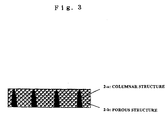
the amorphous silicon film. When the polycrystalline silicon is treated
according to the anodic oxidation method, as shown in Fig. 3, it is possible to
form a porous structure (2-b) in which fine columnar structures (2-a), which
are aggregates of grains (crystal particles), are present and silicon nano-sized
silicon crystals are present among the fine columnar structures. It is
considered that this is because an anodic oxidation reaction of the
polycrystalline silicon progresses preferentially in boundaries of the grains,
that is, anodic oxidation progresses in a depth direction among columns of the
columnar structure, and the columnar silicon grains still remain even after the
anodic oxidation. By adopting such a structure, it is possible to permit heat to
escape to the substrate side efficiently in the part of the columnar structure
while maintaining a macroscopic function as the heat insulation layer.
It is needless to mention that a size and a rate per a unit volume of
presence of the silicon grains of this columnar structure change depending on
conditions of the anodic oxidation. In the invention of this application, such
presence of the silicon grain is presented as a more preferable form.
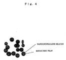
In addition, the inventors of this application paid attention to the fact
that thermal conductivity of SiO2 and Si3N4, which were insulating materials,
was small compared with thermal conductivity of the silicon that was a
skeleton of the porous silicon. In short, as shown in Fig. 4, the inventors
found that it was possible to reduce the thermal conductivity α of the porous
silicon by forming dielectric films on surfaces of nanocrystalline silicon
forming the porous silicon and decreasing thermal conductivity of the skeleton
portions. However, since heat capacities C of these insulating materials is
large compared with that of the silicon, it is necessary to appropriately select a
thickness of the dielectric films to be formed on the surfaces of the silicon
crystals such that the αC value are small.
Although a method of forming these dielectric films is not specifically
limited, it is preferable to form the dielectric films according to, for example,
heat treatment or electrochemical treatment. It is possible to perform the heat
treatment by applying heat under an oxygen atmosphere or a nitrogen
atmosphere. A temperature condition, a temperature rise condition, and the
like at that point are selected appropriately depending on a material of a
substrate to be used or the like. For example, it is possible to perform thermal
oxidation treatment in a temperature range of 800 °C to 950 °C for 0.5 to 5
hours. It is possible to perform the electrochemical oxidation treatment by
feeding a constant current between the substrate and a counter electrode for a
predetermined time in an electrolyte solution such as a sulfuric acid aqueous
solution. It is possible to select a current value, a conducting time, and the
like at that point appropriately according to a thickness of an oxide film
desired to be formed.
As the thermally conductive substrate (1), in order to permit heat of a
DC component to escape, it is preferable to use a material having large thermal
conductivity α and it is most preferable to use metal. For example, substrates
having high thermal conductivity of copper and aluminum are selected.
However, the substrate (1) is not limited to these, and it is possible to use a
semiconductor substrate such as a silicon substrate. In addition, it is also
possible to use a ceramic substrate such as glass. As a form of the substrate, a
heat radiation fin may be formed on a rear surface thereof in order to improve
heat radiation efficiency.
Next, a material for the heating element thin film (3) is not specifically
limited as long as the heating element thin film (3) is a metal film. For
example, single metal such as W, Mo, Ir, Au, Al, Ni, Ti, or Pt or a laminated
structure of these pieces of metal is used. It is possible to form the heating
element thin film (3) according to vacuum evaporation, sputtering, or the like.
In addition, it is preferable to make a thickness of the heating element thin
film (3) as small as possible in order to reduce a heat capacity. However, it is
possible to select the thickness in a range of 10 nm to 100 nm in order to have
an appropriate resistance.
Thus, embodiments will be described below to explain the invention of
this application more in detail. It is needless to mention that the invention is
not limited by the following embodiments.
A film of Al was formed 300 nm as a contact electrode for anodic
oxidation treatment on a rear surface of a P-type (100) single crystalline silicon
substrate (80 to 120 Ωcm) (αSCS=286×106) according to vacuum evaporation.
Thereafter, this substrate was subjected to the anodic oxidation treatment at a
current density of 100 mA/cm2 for eight minutes with platinum as a counter
electrode in a solution of HF(55%):EtOH=1:1 to form a porous silicon layer
(αICI=0.06×10⁶) with a thickness of about 50 µm. Finally, W was formed in a
thickness of 50 nm as a heating element thin film on the porous silicon layer
according to the sputtering method to manufacture an element with an area of
5 mm2.
A layer (αICI=0.26×10⁶) coated with polyimide in a thickness of 50 µm
was formed on an upper surface of a substrate of pure copper (thickness 1 mm)
(αSCS=1393×106). Finally, W was formed in a thickness of 50 nm as a heating
element thin film on the polyimide according to the sputtering method to
manufacture an element with an area of 5 mm2.
An SiO2 layer (α1C1=3.2×10⁶) with a thickness of 2 µm was formed on
an upper surface of a substrate of pure copper (thickness 1 mm)
(αsCs=1393×106) according to the sputtering method. Finally, W was formed
in a thickness of 50 nm as a heating element thin film on the SiO2 according to
the sputtering method to manufacture an element with an area of 5 mm2.
An Al2O3 film (αICI=93×106) with a thickness of 2 µm was formed on
an upper surface of a P-type (100) single crystalline silicon substrate (80 to 120
Ωcm) (αSCS=286×106) according to the sputtering method. Finally, W was
formed in a thickness of 50 nm as a heating element thin film on the Al2O3 film
according to the sputtering method to manufacture an element with an area of
5 mm2.
A layer (αICI=0.0018×10⁶) coated with polystyrene foam in a thickness
of 100 µm was formed on an upper surface of soda glass (αSCS=1393×106) with
a thickness of 1.1 mm. Finally, W was formed in a thickness of 50 nm as a
heating element thin film on the polystyrene foam according to the sputtering
method to manufacture an element with an area of 5 mm2.
Electric power of 50 kHz and 1 W/cm2 was supplied to the heating
element thin films of the elements obtained in the first to the third
embodiments and the first and the second comparative examples to measure
output sound pressures with a microphone at a distance of 10 mm from the
elements.
A result of the measurement is shown in Table 2.
| No. | Substrate | Heat insulation layer | αICI/αsCs | αsCs (×106) | Output sound pressure (Pa) | |
| First embodiment | Silicon | | 1/4764 | 280 | 0.28 | |
| Second | Copper | Polyimide | 1/5358 | 1393 | 0.17 | |
| Third | Copper | SiO | 2 | 1/435 | 1393 | 0.11 |
| First comparative example | Silicon | Al2O3 | 1/3.1 | 280 | 0.01 | |
| Second comparative example | SiO2 | Polystyrene foam | 1/1778 | 3.2 | 0.03 |
Ultrasonic waves of 100 kHz were generated from the respective
elements of the first to the third embodiments and the first and the second
comparative examples. It is seen from Table 2 that a sound pressure increases
for a combination of 1/100≥αICI/αSCS and αSCS≥100×106.
A film of polycrystalline silicon was formed in a thickness of 3 µm on a
surface of a substrate of pure copper with a thickness of 1 mm according to the
plasma CVD method.
Thereafter, this substrate was subjected to the anodic oxidation
treatment at a current density of 20 mA/cm2 for three minutes with platinum as
a counter electrode in a solution of HF(55%):EtOH=1:1 to form a porous
silicon layer. Finally, W was formed in a thickness of 50 nm as a heating
element thin film on the porous silicon layer according to the sputtering
method to manufacture an element with an area of 5 mm2. When the porous
silicon layer of the obtained element was observed, a columnar structure of
silicon grains was observed. Moreover, electric power of 50 kHz and 50 W/cm2
was supplied to the heating element thin film of the obtained element to
measure an output sound pressure with a microphone at a distance of 10 mm
from the element. As a result, generation of an ultrasonic wave of 100 kHz
was confirmed and the sound pressure output was 5.8 Pa. A steady-state
temperature on the surface of the element at that point was about 50 °C.
A film of Al was formed 300 nm as a contact electrode for anodic
oxidation treatment on a rear surface of a P-type (100) single crystalline silicon
substrate (3 to 20 Ωcm) according to vacuum evaporation. Thereafter, this
substrate was subjected to the anodic oxidation treatment at a current density
of 20 mA/cm2 for three minutes with platinum as a counter electrode in a
solution of HF(55%):EtOH=1:1 to form a porous silicon layer with a thickness
of about 3 µm. Finally, W was formed in a thickness of 50 nm as a heating
element thin film on the porous silicon layer according to the sputtering
method to manufacture an element with an area of 5 mm2. When the porous
silicon layer of the obtained element was observed, a columnar structure of
silicon grains was not observed specifically. Moreover, electric power of 50
kHz and 50 W/cm2 was supplied to the heating element thin film of the
obtained element to measure an output sound pressure with a microphone at a
distance of 10 mm from the element. As a result, generation of an ultrasonic
wave of 100 kHz was confirmed and the sound pressure output was 3.8 Pa. A
steady-state temperature on the surface of the element at that point was about
80 °C.
It was also confirmed from the above that, in the thermally induced
sound wave generating device according to the invention of this application, by
using the porous silicon layer, which was formed by making polycrystalline
silicon porous, as the heat insulation layer, since that portion permits heat of a
DC component to escape to the substrate side efficiently, it was possible to
generate sound waves efficiently even for high power output.
A film of Al was formed 300 nm as a contact electrode for anodic
oxidation treatment on a rear surface of a P-type (100) single crystalline silicon
substrate (3 to 20 Ωcm) according to vacuum evaporation. Thereafter, this
substrate was subjected to the anodic oxidation treatment at a current density
of 20 mA/cm2 for forty minutes with platinum as a counter electrode in a
solution of HF(55%):EtOH=1:1 to form a porous silicon layer with a thickness
of about 50 µm. Thereafter, the substrate was subjected to the thermal
oxidation treatment at 900 °C for ten minutes in an oxygen atmosphere to form
dielectric films consisting of SiO2 on surfaces of nanocrystalline silicon.
Finally, W was formed in a thickness of 50 nm as a heating element thin film on
the porous silicon layer according to the sputtering method to manufacture an
element with an area of 5 mm2.
An element was manufactured in the same manner as the fifth
embodiment except that the treatment was performed in a nitrogen atmosphere
as heat treatment to form a dielectric film consisting of Si2N4.
An element was manufacture in the same manner as the fifth
embodiment except that the electrochemical oxidation treatment was
performed to form a dielectric film consisting of SiO2. More specifically, the
treatment was performed at a current density of 5 mA/cm2 for 10 minutes with
a platinum electrode as a counter electrode in a 1M sulfuric acid aqueous
solution.
An element was manufactured in the same manner as the fifth
embodiment except that the thermal oxidation treatment was not performed.
The thermal conductivity α and the heat capacity C of the porous
silicon layer were measured for the fifth to the seventh embodiments and the
fourth comparative example according to an photo-acoustic method. In
addition, electric power of 50 kHz and 1 W/cm2 was supplied to the heating
element thin films of the obtained elements to measure output sound pressures
with a microphone at a distance of 10 mm from the elements.
A result of the measurement is shown in Table 3.
| No. | Thermal conductivity α (W/mk) | Heat capacity C (106 J/m3K) | αC (×106) | Output sound pressure (Pa) |
| Fifth embodiment | 0.1 | 1.2 | 0.12 | 0.25 |
| Sixth embodiment | 0.3 | 1.3 | 0.39 | 0.14 |
| Seventh embodiment | 0.1 | 1.1 | 0.11 | 0.26 |
| Fourth comparative example | 1.1 | 0.7 | 0.77 | 0.10 |
Ultrasonic waves of 100 kHz were generated from the respective
elements. From Table 3, by forming the dielectric layer, although the heat
capacity C increases slightly, the thermal conductivity decreases and, as a
result, a value of αC decreases. Therefore, the output sound pressure to be
generated increased.
Consequently, in the thermally induced sound wave generating device
according to the invention of this application, in the thermally induced sound
wave generating device including the thermally conductive substrate, the heat
insulation layer consisting of the porous silicon layer formed on one surface on
the substrate, and the heating element thin film consisting of a metal film that
is formed on the heat insulation layer and driven electrically, by forming the
insulating film on the surfaces of the silicon crystals of the porous silicon layer,
it is possible to decrease the thermal conductivity α in the heat insulation layer
and it is possible to increase a generated sound pressure.
As described above in detail, in the thermally induced sound wave
generating device according to the invention of this application, the thermally
induced sound wave generating device includes: the thermally conductive
substrate; the heat insulation layer formed on one surface of the substrate; and
the heating element thin film consisting of a metal film that is formed on the
heat insulation layer and driven electrically, and, when thermal conductivity of
the thermally conductive substrate is set as αS, a heat capacity thereof is set as
CS, thermal conductivity of the heat insulation layer is set as αI, and a heat
capacity thereof is set as CI, materials for the thermally conductive substrate
and the heat insulation layer are selected such that a relation of
1/100≥αICI/αSCS and αSCS≥100×106 is realized. Consequently, it is possible to
improve an output sound pressure characteristic significantly.
In addition, in the thermally induced sound wave generating device
according to the invention of this application, the porous silicon layer, which is
formed by making polycrystalline silicon porous, is used as the heat insulation
layer. Consequently, since the silicon grains of the columnar structure permit
heat of a DC component to escape to the substrate side efficiently, it is possible
to generate sound waves efficiently even for high power output.
Further, in the thermally induced sound wave generating device
according to the invention of this application, in the thermally induced sound
generating device including: the thermally conductive substrate; the heat
insulation layer consisting of the porous silicon layer that is formed on one
surface on the substrate; and the heating element thin film consisting of a
metal film that is formed on the heat insulation layer and driven electrically,
dielectric films are formed on surfaces of nanocrystalline silicon of the porous
silicon layer. Consequently, it is possible to decrease thermal conductivity α
in a heat insulation layer and it is possible to increase a generated sound
pressure.
Claims (10)
- A thermally induced sound wave generating device comprising: a thermally conductive substrate; a heat insulation layer formed on one surface of the substrate; and a heating element thin film formed on the heat insulation layer and in the form of an electrically driven metal film, and wherein when thermal conductivity of the thermally conductive substrate is set as αS and its heat capacity is set as CS, and thermal conductivity of the heat insulation layer is set as αI and its heat capacity is set as CI, relation of 1/100≥αICI/αSCS and αSCS≥100×106 is realized.
- A thermally induced sound wave generating device according to claim 1, characterized in that the thermally conductive substrate consists of a semiconductor or metal.
- A thermally induced sound wave generating device according to claim 1, characterized in that the thermally conductive substrate consists of a ceramics substrate.
- A thermally induced sound wave generating device according to claim 1, characterized in that the heat insulation layer is a porous silicon layer that is formed on one surface of the thermally conductive substrate by making polycrystalline silicon porous.
- A thermally induced sound wave generating device according to claim 4, characterized in that the porous silicon layer has silicon grains of a columnar structure at least in a part in the porous silicon layer.
- A thermally induced sound wave generating device according to claim 4 or 5, characterized in that, in the porous silicon layer, dielectric films are formed on surfaces of nanocrystalline silicon.
- A thermally induced sound wave generating device according to claim 6, characterized in that the dielectric films are oxide films.
- A thermally induced sound wave generating device according to claim 6, characterized in that the dielectric films are nitride films.
- A thermally induced sound wave generating device according to any one of claims 6 to 9, characterized in that the dielectric films are formed according to heat treatment.
- A thermally induced sound wave generating device according to any one of claims 6 to 9, characterized in that the dielectric films are formed according to electrochemical treatment.
Applications Claiming Priority (7)
| Application Number | Priority Date | Filing Date | Title |
|---|---|---|---|
| JP2003053282 | 2003-02-28 | ||
| JP2003053283 | 2003-02-28 | ||
| JP2003053281 | 2003-02-28 | ||
| JP2003053282 | 2003-02-28 | ||
| JP2003053281 | 2003-02-28 | ||
| JP2003053283 | 2003-02-28 | ||
| PCT/JP2004/002382 WO2004077881A1 (en) | 2003-02-28 | 2004-02-27 | Thermally excited sound wave generating device |
Publications (2)
| Publication Number | Publication Date |
|---|---|
| EP1599068A1 true EP1599068A1 (en) | 2005-11-23 |
| EP1599068A4 EP1599068A4 (en) | 2009-04-22 |
Family
ID=32931134
Family Applications (1)
| Application Number | Title | Priority Date | Filing Date |
|---|---|---|---|
| EP04715490A Withdrawn EP1599068A4 (en) | 2003-02-28 | 2004-02-27 | SOURCE WAVE GENERATION DEVICE WITH THERMIC EXCITATION |
Country Status (5)
| Country | Link |
|---|---|
| US (1) | US20050201575A1 (en) |
| EP (1) | EP1599068A4 (en) |
| JP (1) | JP3808493B2 (en) |
| KR (2) | KR20060095582A (en) |
| WO (1) | WO2004077881A1 (en) |
Cited By (3)
| Publication number | Priority date | Publication date | Assignee | Title |
|---|---|---|---|---|
| EP1761105A4 (en) * | 2004-04-28 | 2009-10-21 | Panasonic Elec Works Co Ltd | PRESSURE GENERATOR AND MANUFACTURING METHOD THEREFOR |
| CN102056066A (en) * | 2009-11-02 | 2011-05-11 | Nxp股份有限公司 | Thermo-acoustic loudspeaker |
| DE102014101287A1 (en) * | 2014-02-03 | 2015-08-06 | Bundesrepublik Deutschland, Vertreten Durch Den Bundesminister Für Wirtschaft Und Energie, Dieser Vertreten Durch Den Präsidenten Der Bundesanstalt Für Materialforschung Und -Prüfung (Bam) | Thermoacoustic ultrasonic transducer |
Families Citing this family (61)
| Publication number | Priority date | Publication date | Assignee | Title |
|---|---|---|---|---|
| JP4649929B2 (en) * | 2004-09-27 | 2011-03-16 | パナソニック電工株式会社 | Pressure wave generator |
| JP4534625B2 (en) * | 2004-06-25 | 2010-09-01 | パナソニック電工株式会社 | Pressure wave generator |
| JP4649889B2 (en) * | 2004-06-25 | 2011-03-16 | パナソニック電工株式会社 | Pressure wave generator |
| JP2006220636A (en) * | 2004-07-27 | 2006-08-24 | Matsushita Electric Works Ltd | Sonic wave sensor |
| JP4682573B2 (en) * | 2004-09-27 | 2011-05-11 | パナソニック電工株式会社 | Pressure wave generator |
| JP2006217059A (en) * | 2005-02-01 | 2006-08-17 | Matsushita Electric Works Ltd | Pressure wave generator |
| JP5221864B2 (en) * | 2005-10-26 | 2013-06-26 | パナソニック株式会社 | Pressure wave generator and manufacturing method thereof |
| WO2007049496A1 (en) | 2005-10-26 | 2007-05-03 | Matsushita Electric Works, Ltd. | Pressure wave generator and process for producing the same |
| US8253578B2 (en) * | 2006-05-12 | 2012-08-28 | Panasonic Corporation | Smoke sensor of the sound wave type including a smoke density estimation unit |
| EP2021706B1 (en) * | 2006-05-30 | 2016-10-12 | LG Electronics, Inc. | Refrigerator |
| JP5116269B2 (en) * | 2006-08-25 | 2013-01-09 | 株式会社ジャパンディスプレイイースト | Image display device |
| JP4817464B2 (en) * | 2006-09-05 | 2011-11-16 | パイオニア株式会社 | Thermoacoustic generator |
| WO2008057004A1 (en) * | 2006-11-10 | 2008-05-15 | Sergey Vladimirovich Shishov | Method for converting electric signals into acoustic oscillations and a multi-functional electric gas-kinetic transducer |
| JP4974672B2 (en) * | 2006-12-28 | 2012-07-11 | 東京エレクトロン株式会社 | Pressure wave generator |
| US9157152B2 (en) * | 2007-03-29 | 2015-10-13 | Tokyo Electron Limited | Vapor deposition system |
| US20090226614A1 (en) * | 2008-03-04 | 2009-09-10 | Tokyo Electron Limited | Porous gas heating device for a vapor deposition system |
| US8068624B2 (en) * | 2008-04-28 | 2011-11-29 | Beijing Funate Innovation Technology Co., Ltd. | Thermoacoustic device |
| US8259968B2 (en) * | 2008-04-28 | 2012-09-04 | Tsinghua University | Thermoacoustic device |
| US8270639B2 (en) * | 2008-04-28 | 2012-09-18 | Tsinghua University | Thermoacoustic device |
| US8249279B2 (en) * | 2008-04-28 | 2012-08-21 | Beijing Funate Innovation Technology Co., Ltd. | Thermoacoustic device |
| US8259967B2 (en) * | 2008-04-28 | 2012-09-04 | Tsinghua University | Thermoacoustic device |
| US8452031B2 (en) * | 2008-04-28 | 2013-05-28 | Tsinghua University | Ultrasonic thermoacoustic device |
| EP2138998B1 (en) * | 2008-06-04 | 2019-11-06 | Tsing Hua University | Thermoacoustic device comprising a carbon nanotube structure |
| CN101656907B (en) * | 2008-08-22 | 2013-03-20 | 清华大学 | Sound box |
| CN101715155B (en) * | 2008-10-08 | 2013-07-03 | 清华大学 | Earphone |
| CN101715160B (en) * | 2008-10-08 | 2013-02-13 | 清华大学 | Flexible sound producing device and sound producing flag |
| US8325947B2 (en) * | 2008-12-30 | 2012-12-04 | Bejing FUNATE Innovation Technology Co., Ltd. | Thermoacoustic device |
| US8300855B2 (en) * | 2008-12-30 | 2012-10-30 | Beijing Funate Innovation Technology Co., Ltd. | Thermoacoustic module, thermoacoustic device, and method for making the same |
| CN101771922B (en) * | 2008-12-30 | 2013-04-24 | 清华大学 | Sounding device |
| TWI382771B (en) * | 2009-01-16 | 2013-01-11 | Beijing Funate Innovation Tech | Thermoacoustic device |
| JP4688977B2 (en) | 2009-06-08 | 2011-05-25 | パナソニック株式会社 | SOUND GENERATOR, ITS MANUFACTURING METHOD, AND SOUND GENERATION METHOD USING SOUND GENERATOR |
| CN101922755A (en) * | 2009-06-09 | 2010-12-22 | 清华大学 | Heating wall |
| CN101943850B (en) * | 2009-07-03 | 2013-04-24 | 清华大学 | Sound-producing screen and projection system using same |
| CN101990152B (en) * | 2009-08-07 | 2013-08-28 | 清华大学 | Thermal sounding device and manufacturing method thereof |
| CN102006542B (en) * | 2009-08-28 | 2014-03-26 | 清华大学 | Sound generating device |
| CN102023297B (en) * | 2009-09-11 | 2015-01-21 | 清华大学 | Sonar system |
| CN102034467B (en) * | 2009-09-25 | 2013-01-30 | 北京富纳特创新科技有限公司 | Sound device |
| CN102056064B (en) * | 2009-11-06 | 2013-11-06 | 清华大学 | Loudspeaker |
| CN102056065B (en) * | 2009-11-10 | 2014-11-12 | 北京富纳特创新科技有限公司 | Sound production device |
| CN102065363B (en) * | 2009-11-16 | 2013-11-13 | 北京富纳特创新科技有限公司 | Sound production device |
| CN106131761B (en) * | 2010-05-10 | 2020-12-29 | 北京富纳特创新科技有限公司 | Thermoacoustic device |
| TWI500331B (en) * | 2010-05-18 | 2015-09-11 | Beijing Funate Innovation Tech | Thermal sounding device |
| KR101989155B1 (en) * | 2012-08-01 | 2019-06-17 | 삼성전자주식회사 | The ultrasonic wave converter, the ultrasonic wave generating apparatus and system including the same |
| CN103841481B (en) | 2012-11-20 | 2017-04-05 | 清华大学 | Earphone |
| CN103841501B (en) | 2012-11-20 | 2017-10-24 | 清华大学 | sound chip |
| CN103841482B (en) | 2012-11-20 | 2017-01-25 | 清华大学 | Earphone set |
| CN103841478B (en) | 2012-11-20 | 2017-08-08 | 清华大学 | Earphone |
| CN103841480B (en) | 2012-11-20 | 2017-04-26 | 清华大学 | Earphone |
| CN103841479B (en) | 2012-11-20 | 2017-08-08 | 清华大学 | earphone |
| CN103841506B (en) | 2012-11-20 | 2017-09-01 | 清华大学 | The preparation method of thermophone array |
| CN103841503B (en) | 2012-11-20 | 2017-12-01 | 清华大学 | sound chip |
| CN103841483B (en) | 2012-11-20 | 2018-03-02 | 清华大学 | earphone |
| CN103841500B (en) | 2012-11-20 | 2018-01-30 | 清华大学 | Thermo-acoustic device |
| CN103841502B (en) | 2012-11-20 | 2017-10-24 | 清华大学 | sound-producing device |
| JP5671101B2 (en) * | 2012-11-20 | 2015-02-18 | ツィンファ ユニバーシティ | Thermoacoustic device and thermoacoustic device array |
| CN103841507B (en) | 2012-11-20 | 2017-05-17 | 清华大学 | Preparation method for thermotropic sound-making device |
| CN103841504B (en) | 2012-11-20 | 2017-12-01 | 清华大学 | Thermophone array |
| US9635468B2 (en) | 2013-03-15 | 2017-04-25 | Board Of Regents, The University Of Texas System | Encapsulated thermoacoustic projector based on freestanding carbon nanotube film |
| US11005263B2 (en) * | 2017-09-27 | 2021-05-11 | Semiconductor Components Industries, Llc | Electro-static discharge (ESD) protection clamp technology |
| EP3724589A4 (en) | 2017-12-14 | 2021-09-01 | Space Charge, LLC | THERMIONIC WAVE GENERATOR (TWG) |
| CN112189347B (en) * | 2018-05-18 | 2022-10-04 | 美商楼氏电子有限公司 | Microphone assembly and method of forming a microphone assembly |
Family Cites Families (6)
| Publication number | Priority date | Publication date | Assignee | Title |
|---|---|---|---|---|
| US4638328A (en) * | 1986-05-01 | 1987-01-20 | Xerox Corporation | Printhead for an ink jet printer |
| JPH03140100A (en) * | 1989-10-26 | 1991-06-14 | Fuji Xerox Co Ltd | Electroacoustic transducing method and apparatus therefor |
| US5515684A (en) * | 1994-09-27 | 1996-05-14 | Macrosonix Corporation | Resonant macrosonic synthesis |
| JP3705926B2 (en) * | 1998-04-23 | 2005-10-12 | 独立行政法人科学技術振興機構 | Pressure wave generator |
| JP2002186097A (en) * | 2000-12-15 | 2002-06-28 | Pioneer Electronic Corp | Speaker |
| US6831394B2 (en) * | 2002-12-11 | 2004-12-14 | General Electric Company | Backing material for micromachined ultrasonic transducer devices |
-
2004
- 2004-02-27 US US10/524,585 patent/US20050201575A1/en not_active Abandoned
- 2004-02-27 WO PCT/JP2004/002382 patent/WO2004077881A1/en not_active Ceased
- 2004-02-27 KR KR1020067016374A patent/KR20060095582A/en not_active Withdrawn
- 2004-02-27 KR KR1020057002570A patent/KR100685684B1/en not_active Expired - Fee Related
- 2004-02-27 EP EP04715490A patent/EP1599068A4/en not_active Withdrawn
- 2004-02-27 JP JP2005502953A patent/JP3808493B2/en not_active Expired - Fee Related
Cited By (6)
| Publication number | Priority date | Publication date | Assignee | Title |
|---|---|---|---|---|
| EP1761105A4 (en) * | 2004-04-28 | 2009-10-21 | Panasonic Elec Works Co Ltd | PRESSURE GENERATOR AND MANUFACTURING METHOD THEREFOR |
| CN102056066A (en) * | 2009-11-02 | 2011-05-11 | Nxp股份有限公司 | Thermo-acoustic loudspeaker |
| EP2326106A1 (en) | 2009-11-02 | 2011-05-25 | Nxp B.V. | Thermo-acoustic loudspeaker |
| CN102056066B (en) * | 2009-11-02 | 2015-04-08 | 楼氏电子亚洲有限公司 | Thermo-acoustic loudspeaker |
| DE102014101287A1 (en) * | 2014-02-03 | 2015-08-06 | Bundesrepublik Deutschland, Vertreten Durch Den Bundesminister Für Wirtschaft Und Energie, Dieser Vertreten Durch Den Präsidenten Der Bundesanstalt Für Materialforschung Und -Prüfung (Bam) | Thermoacoustic ultrasonic transducer |
| DE102014101287B4 (en) * | 2014-02-03 | 2017-09-21 | Bundesrepublik Deutschland, Vertreten Durch Den Bundesminister Für Wirtschaft Und Energie, Dieser Vertreten Durch Den Präsidenten Der Bundesanstalt Für Materialforschung Und -Prüfung (Bam) | Thermoacoustic ultrasonic transducer |
Also Published As
| Publication number | Publication date |
|---|---|
| KR20060095582A (en) | 2006-08-31 |
| EP1599068A4 (en) | 2009-04-22 |
| KR20050047101A (en) | 2005-05-19 |
| JPWO2004077881A1 (en) | 2006-06-08 |
| KR100685684B1 (en) | 2007-02-26 |
| US20050201575A1 (en) | 2005-09-15 |
| WO2004077881A1 (en) | 2004-09-10 |
| JP3808493B2 (en) | 2006-08-09 |
Similar Documents
| Publication | Publication Date | Title |
|---|---|---|
| EP1599068A1 (en) | Thermally excited sound wave generating device | |
| JP3705926B2 (en) | Pressure wave generator | |
| JP6937404B2 (en) | Pre-equilibrium systems and methods using nanodesign porous network structural materials and solid-state devices as energy transducers | |
| CN1698400A (en) | Thermally excited sound wave generating device | |
| WO2008056466A1 (en) | Power generation method employing thermal power generation element, thermal power generation element and method for fabricating the same | |
| TW200300367A (en) | Thermally induced pressure wave generation apparatus | |
| JP4513546B2 (en) | Pressure wave generating element and manufacturing method thereof | |
| TWI243496B (en) | Piezoelectric film element, method of manufacturing the same, and liquid discharge head | |
| JP3845077B2 (en) | Method for manufacturing sound wave generator | |
| WO2019201521A1 (en) | Bulk acoustic wave resonator and method for manufacturing the same | |
| JP3865736B2 (en) | Ultrasonic sound source and ultrasonic sensor | |
| JP2007054831A (en) | Ultrasonic sound source and ultrasonic sensor | |
| JP2006217059A (en) | Pressure wave generator | |
| US11838726B2 (en) | Pressure wave-generating device and method for producing the same | |
| Hirota et al. | Generation of radiation pressure in thermally induced ultrasonic emitter based on nanocrystalline silicon | |
| JP2023109680A (en) | Crystalline film, laminated structure, electronic device, electronic equipment, and manufacturing method thereof | |
| US12280399B2 (en) | Method for manufacturing an acoustic wave transducing unit | |
| TWI401122B (en) | Pressure wave generating device and temperature adjusting method thereof | |
| KR20160069961A (en) | Energy harvesting device, electrocaloric cooling device, method of fabricating the devices and monolithic device having the devices | |
| WO2023145808A1 (en) | Crystal, multilayer structure, electronic device, electronic instrument, and methods respectively for producing these products | |
| JP7651229B2 (en) | Laminated structure, electronic device, electronic equipment and system | |
| JP7651230B2 (en) | Laminated structure, electronic device, electronic equipment and system | |
| US20250011970A1 (en) | Laminated structure, electronic device, electronic apparatus, and method for manufacturing the same | |
| JP2023109682A (en) | Shape memory material, laminated structure, electronic device, electronic equipment, and manufacturing method thereof | |
| JP2024081176A (en) | Film deposition apparatus |
Legal Events
| Date | Code | Title | Description |
|---|---|---|---|
| PUAI | Public reference made under article 153(3) epc to a published international application that has entered the european phase |
Free format text: ORIGINAL CODE: 0009012 |
|
| 17P | Request for examination filed |
Effective date: 20050215 |
|
| AK | Designated contracting states |
Kind code of ref document: A1 Designated state(s): AT BE BG CH CY CZ DE DK EE ES FI FR GB GR HU IE IT LI LU MC NL PT RO SE SI SK TR |
|
| AX | Request for extension of the european patent |
Extension state: AL LT LV MK |
|
| DAX | Request for extension of the european patent (deleted) | ||
| RBV | Designated contracting states (corrected) |
Designated state(s): DE FR GB |
|
| A4 | Supplementary search report drawn up and despatched |
Effective date: 20090319 |
|
| STAA | Information on the status of an ep patent application or granted ep patent |
Free format text: STATUS: THE APPLICATION IS DEEMED TO BE WITHDRAWN |
|
| 18D | Application deemed to be withdrawn |
Effective date: 20090618 |