EP1598859A1 - Substrate processing method - Google Patents
Substrate processing method Download PDFInfo
- Publication number
- EP1598859A1 EP1598859A1 EP04713215A EP04713215A EP1598859A1 EP 1598859 A1 EP1598859 A1 EP 1598859A1 EP 04713215 A EP04713215 A EP 04713215A EP 04713215 A EP04713215 A EP 04713215A EP 1598859 A1 EP1598859 A1 EP 1598859A1
- Authority
- EP
- European Patent Office
- Prior art keywords
- plasma
- substrate
- processing method
- oxide film
- processing
- Prior art date
- Legal status (The legal status is an assumption and is not a legal conclusion. Google has not performed a legal analysis and makes no representation as to the accuracy of the status listed.)
- Withdrawn
Links
Images



Classifications
-
- H—ELECTRICITY
- H10—SEMICONDUCTOR DEVICES; ELECTRIC SOLID-STATE DEVICES NOT OTHERWISE PROVIDED FOR
- H10P—GENERIC PROCESSES OR APPARATUS FOR THE MANUFACTURE OR TREATMENT OF DEVICES COVERED BY CLASS H10
- H10P14/00—Formation of materials, e.g. in the shape of layers or pillars
- H10P14/60—Formation of materials, e.g. in the shape of layers or pillars of insulating materials
- H10P14/65—Formation of materials, e.g. in the shape of layers or pillars of insulating materials characterised by treatments performed before or after the formation of the materials
- H10P14/6502—Formation of materials, e.g. in the shape of layers or pillars of insulating materials characterised by treatments performed before or after the formation of the materials of treatments performed before formation of the materials
- H10P14/6512—Formation of materials, e.g. in the shape of layers or pillars of insulating materials characterised by treatments performed before or after the formation of the materials of treatments performed before formation of the materials by exposure to a gas or vapour
- H10P14/6514—Formation of materials, e.g. in the shape of layers or pillars of insulating materials characterised by treatments performed before or after the formation of the materials of treatments performed before formation of the materials by exposure to a gas or vapour by exposure to a plasma
-
- H—ELECTRICITY
- H10—SEMICONDUCTOR DEVICES; ELECTRIC SOLID-STATE DEVICES NOT OTHERWISE PROVIDED FOR
- H10P—GENERIC PROCESSES OR APPARATUS FOR THE MANUFACTURE OR TREATMENT OF DEVICES COVERED BY CLASS H10
- H10P14/00—Formation of materials, e.g. in the shape of layers or pillars
- H10P14/60—Formation of materials, e.g. in the shape of layers or pillars of insulating materials
-
- H—ELECTRICITY
- H10—SEMICONDUCTOR DEVICES; ELECTRIC SOLID-STATE DEVICES NOT OTHERWISE PROVIDED FOR
- H10P—GENERIC PROCESSES OR APPARATUS FOR THE MANUFACTURE OR TREATMENT OF DEVICES COVERED BY CLASS H10
- H10P14/00—Formation of materials, e.g. in the shape of layers or pillars
- H10P14/60—Formation of materials, e.g. in the shape of layers or pillars of insulating materials
- H10P14/63—Formation of materials, e.g. in the shape of layers or pillars of insulating materials characterised by the formation processes
- H10P14/6302—Non-deposition formation processes
- H10P14/6318—Formation by simultaneous oxidation and nitridation
-
- H—ELECTRICITY
- H10—SEMICONDUCTOR DEVICES; ELECTRIC SOLID-STATE DEVICES NOT OTHERWISE PROVIDED FOR
- H10P—GENERIC PROCESSES OR APPARATUS FOR THE MANUFACTURE OR TREATMENT OF DEVICES COVERED BY CLASS H10
- H10P14/00—Formation of materials, e.g. in the shape of layers or pillars
- H10P14/60—Formation of materials, e.g. in the shape of layers or pillars of insulating materials
- H10P14/65—Formation of materials, e.g. in the shape of layers or pillars of insulating materials characterised by treatments performed before or after the formation of the materials
- H10P14/6516—Formation of materials, e.g. in the shape of layers or pillars of insulating materials characterised by treatments performed before or after the formation of the materials of treatments performed after formation of the materials
- H10P14/6518—Formation of materials, e.g. in the shape of layers or pillars of insulating materials characterised by treatments performed before or after the formation of the materials of treatments performed after formation of the materials by introduction of substances into an already-existing insulating layer
- H10P14/6519—Formation of materials, e.g. in the shape of layers or pillars of insulating materials characterised by treatments performed before or after the formation of the materials of treatments performed after formation of the materials by introduction of substances into an already-existing insulating layer the substance being oxygen
-
- H—ELECTRICITY
- H10—SEMICONDUCTOR DEVICES; ELECTRIC SOLID-STATE DEVICES NOT OTHERWISE PROVIDED FOR
- H10P—GENERIC PROCESSES OR APPARATUS FOR THE MANUFACTURE OR TREATMENT OF DEVICES COVERED BY CLASS H10
- H10P14/00—Formation of materials, e.g. in the shape of layers or pillars
- H10P14/60—Formation of materials, e.g. in the shape of layers or pillars of insulating materials
- H10P14/65—Formation of materials, e.g. in the shape of layers or pillars of insulating materials characterised by treatments performed before or after the formation of the materials
- H10P14/6516—Formation of materials, e.g. in the shape of layers or pillars of insulating materials characterised by treatments performed before or after the formation of the materials of treatments performed after formation of the materials
- H10P14/6518—Formation of materials, e.g. in the shape of layers or pillars of insulating materials characterised by treatments performed before or after the formation of the materials of treatments performed after formation of the materials by introduction of substances into an already-existing insulating layer
- H10P14/6524—Formation of materials, e.g. in the shape of layers or pillars of insulating materials characterised by treatments performed before or after the formation of the materials of treatments performed after formation of the materials by introduction of substances into an already-existing insulating layer the substance being nitrogen
- H10P14/6526—Formation of materials, e.g. in the shape of layers or pillars of insulating materials characterised by treatments performed before or after the formation of the materials of treatments performed after formation of the materials by introduction of substances into an already-existing insulating layer the substance being nitrogen introduced into an oxide material, e.g. changing SiO to SiON
-
- H—ELECTRICITY
- H10—SEMICONDUCTOR DEVICES; ELECTRIC SOLID-STATE DEVICES NOT OTHERWISE PROVIDED FOR
- H10P—GENERIC PROCESSES OR APPARATUS FOR THE MANUFACTURE OR TREATMENT OF DEVICES COVERED BY CLASS H10
- H10P14/00—Formation of materials, e.g. in the shape of layers or pillars
- H10P14/60—Formation of materials, e.g. in the shape of layers or pillars of insulating materials
- H10P14/65—Formation of materials, e.g. in the shape of layers or pillars of insulating materials characterised by treatments performed before or after the formation of the materials
- H10P14/6516—Formation of materials, e.g. in the shape of layers or pillars of insulating materials characterised by treatments performed before or after the formation of the materials of treatments performed after formation of the materials
- H10P14/6529—Formation of materials, e.g. in the shape of layers or pillars of insulating materials characterised by treatments performed before or after the formation of the materials of treatments performed after formation of the materials by exposure to a gas or vapour
- H10P14/6532—Formation of materials, e.g. in the shape of layers or pillars of insulating materials characterised by treatments performed before or after the formation of the materials of treatments performed after formation of the materials by exposure to a gas or vapour by exposure to a plasma
-
- H—ELECTRICITY
- H10—SEMICONDUCTOR DEVICES; ELECTRIC SOLID-STATE DEVICES NOT OTHERWISE PROVIDED FOR
- H10P—GENERIC PROCESSES OR APPARATUS FOR THE MANUFACTURE OR TREATMENT OF DEVICES COVERED BY CLASS H10
- H10P14/00—Formation of materials, e.g. in the shape of layers or pillars
- H10P14/60—Formation of materials, e.g. in the shape of layers or pillars of insulating materials
- H10P14/69—Inorganic materials
- H10P14/692—Inorganic materials composed of oxides, glassy oxides or oxide-based glasses
- H10P14/6921—Inorganic materials composed of oxides, glassy oxides or oxide-based glasses containing silicon
- H10P14/69215—Inorganic materials composed of oxides, glassy oxides or oxide-based glasses containing silicon the material being a silicon oxide, e.g. SiO2
-
- H—ELECTRICITY
- H10—SEMICONDUCTOR DEVICES; ELECTRIC SOLID-STATE DEVICES NOT OTHERWISE PROVIDED FOR
- H10P—GENERIC PROCESSES OR APPARATUS FOR THE MANUFACTURE OR TREATMENT OF DEVICES COVERED BY CLASS H10
- H10P14/00—Formation of materials, e.g. in the shape of layers or pillars
- H10P14/60—Formation of materials, e.g. in the shape of layers or pillars of insulating materials
- H10P14/69—Inorganic materials
- H10P14/692—Inorganic materials composed of oxides, glassy oxides or oxide-based glasses
- H10P14/6921—Inorganic materials composed of oxides, glassy oxides or oxide-based glasses containing silicon
- H10P14/6922—Inorganic materials composed of oxides, glassy oxides or oxide-based glasses containing silicon the material containing Si, O and at least one of H, N, C, F or other non-metal elements, e.g. SiOC, SiOC:H or SiONC
- H10P14/6927—Inorganic materials composed of oxides, glassy oxides or oxide-based glasses containing silicon the material containing Si, O and at least one of H, N, C, F or other non-metal elements, e.g. SiOC, SiOC:H or SiONC the material being a silicon oxynitride, e.g. SiON or SiON:H
-
- H—ELECTRICITY
- H10—SEMICONDUCTOR DEVICES; ELECTRIC SOLID-STATE DEVICES NOT OTHERWISE PROVIDED FOR
- H10P—GENERIC PROCESSES OR APPARATUS FOR THE MANUFACTURE OR TREATMENT OF DEVICES COVERED BY CLASS H10
- H10P14/00—Formation of materials, e.g. in the shape of layers or pillars
- H10P14/60—Formation of materials, e.g. in the shape of layers or pillars of insulating materials
- H10P14/69—Inorganic materials
- H10P14/694—Inorganic materials composed of nitrides
- H10P14/6943—Inorganic materials composed of nitrides containing silicon
- H10P14/69433—Inorganic materials composed of nitrides containing silicon the material being a silicon nitride not containing oxygen, e.g. SixNy or SixByNz
-
- H—ELECTRICITY
- H10—SEMICONDUCTOR DEVICES; ELECTRIC SOLID-STATE DEVICES NOT OTHERWISE PROVIDED FOR
- H10P—GENERIC PROCESSES OR APPARATUS FOR THE MANUFACTURE OR TREATMENT OF DEVICES COVERED BY CLASS H10
- H10P50/00—Etching of wafers, substrates or parts of devices
- H10P50/20—Dry etching; Plasma etching; Reactive-ion etching
- H10P50/24—Dry etching; Plasma etching; Reactive-ion etching of semiconductor materials
- H10P50/242—Dry etching; Plasma etching; Reactive-ion etching of semiconductor materials of Group IV materials
-
- H—ELECTRICITY
- H10—SEMICONDUCTOR DEVICES; ELECTRIC SOLID-STATE DEVICES NOT OTHERWISE PROVIDED FOR
- H10P—GENERIC PROCESSES OR APPARATUS FOR THE MANUFACTURE OR TREATMENT OF DEVICES COVERED BY CLASS H10
- H10P70/00—Cleaning of wafers, substrates or parts of devices
- H10P70/10—Cleaning before device manufacture, i.e. Begin-Of-Line process
- H10P70/12—Cleaning before device manufacture, i.e. Begin-Of-Line process by dry cleaning only
-
- H—ELECTRICITY
- H10—SEMICONDUCTOR DEVICES; ELECTRIC SOLID-STATE DEVICES NOT OTHERWISE PROVIDED FOR
- H10P—GENERIC PROCESSES OR APPARATUS FOR THE MANUFACTURE OR TREATMENT OF DEVICES COVERED BY CLASS H10
- H10P14/00—Formation of materials, e.g. in the shape of layers or pillars
- H10P14/60—Formation of materials, e.g. in the shape of layers or pillars of insulating materials
- H10P14/63—Formation of materials, e.g. in the shape of layers or pillars of insulating materials characterised by the formation processes
- H10P14/6302—Non-deposition formation processes
- H10P14/6304—Formation by oxidation, e.g. oxidation of the substrate
- H10P14/6306—Formation by oxidation, e.g. oxidation of the substrate of the semiconductor materials
- H10P14/6308—Formation by oxidation, e.g. oxidation of the substrate of the semiconductor materials of Group IV semiconductors
- H10P14/6309—Formation by oxidation, e.g. oxidation of the substrate of the semiconductor materials of Group IV semiconductors of silicon in uncombined form, i.e. pure silicon
-
- H—ELECTRICITY
- H10—SEMICONDUCTOR DEVICES; ELECTRIC SOLID-STATE DEVICES NOT OTHERWISE PROVIDED FOR
- H10P—GENERIC PROCESSES OR APPARATUS FOR THE MANUFACTURE OR TREATMENT OF DEVICES COVERED BY CLASS H10
- H10P14/00—Formation of materials, e.g. in the shape of layers or pillars
- H10P14/60—Formation of materials, e.g. in the shape of layers or pillars of insulating materials
- H10P14/63—Formation of materials, e.g. in the shape of layers or pillars of insulating materials characterised by the formation processes
- H10P14/6302—Non-deposition formation processes
- H10P14/6316—Formation by nitridation, e.g. nitridation of the substrate
-
- H—ELECTRICITY
- H10—SEMICONDUCTOR DEVICES; ELECTRIC SOLID-STATE DEVICES NOT OTHERWISE PROVIDED FOR
- H10P—GENERIC PROCESSES OR APPARATUS FOR THE MANUFACTURE OR TREATMENT OF DEVICES COVERED BY CLASS H10
- H10P14/00—Formation of materials, e.g. in the shape of layers or pillars
- H10P14/60—Formation of materials, e.g. in the shape of layers or pillars of insulating materials
- H10P14/63—Formation of materials, e.g. in the shape of layers or pillars of insulating materials characterised by the formation processes
- H10P14/6302—Non-deposition formation processes
- H10P14/6319—Formation by plasma treatments, e.g. plasma oxidation of the substrate
Definitions
- the present invention generally relates to substrate processing technology, and more particularly to a substrate processing method for forming an insulation film on a silicon substrate.
- high quality silicon oxide films used for the gate insulation film of a MOS transistor have been formed by thermal oxidation processing of a silicon substrate surface.
- a thermal oxide film of silicon thus formed has the feature of small number of dangling bonds, and there is caused little trapping of carriers even in the case the film is used for an insulation film covering the channel region and thus used in the environment in which the film is subjected to high electric field. Thereby, stable threshold characteristics are realized.
- the silicon oxide film thus formed by microwave plasma oxidation of silicon substrate it has been confirmed that leakage current of 1 ⁇ 10 -2 A/cm 2 is possible with the application voltage of 1V, even in the case the film has a film thickness of 1.5nm.
- the silicon oxide film formed by microwave plasma enables breaking through of the foregoing limit of device miniaturization encountered in the conventional semiconductor devices that use a conventional thermal oxide film.
- the substrate processing that uses the microwave plasma it becomes possible to form an oxynitride film or nitride having a large specific dielectric constant on a silicon substrate with the film quality exceeding the film quality of a thermal oxide film.
- a leakage current of 1 ⁇ 10 -2 A/cm 2 or less is realized at the application voltage of 1V for an oxynitride film having a film thickness equivalent to the film thickness of 1nm of silicon oxide film.
- Substrate processing by microwave plasma can be performed at a low temperature typically below 500°C, and because of this, it becomes possible to reduce the time needed for raising and lowering the substrate temperature. Thereby, it becomes possible to produce the semiconductor device with large throughput. Further, with such low temperature processing, there occurs no change of impurity concentration profile of diffusion regions even when the diffusion regions are already formed in the substrate, and it becomes possible to realize desired device characteristics with reliability.
- a gate insulation film is required to provide the feature of small leakage current and high reliability.
- Figure 1 shows the relationship between the accumulated defect rate F and integral electric charge amount (Qbd) leading to breakdown (TDDB characteristic) for a silicon oxide film formed on a silicon substrate surface with the thickness of 10nm by a microwave plasma oxidation processing conducted by the inventor of the present invention (shown in the drawing as "plasma oxide film”), in comparison with a thermal oxide film of the same thickness, wherein the vertical axis represents the accumulated defect rate F while the horizontal axis represents the integral electric charge amount Qbd that leads to insulation breakdown.
- plasma oxide film integral electric charge amount leading to breakdown
- the plasma oxide film has been formed by using a microwave plasma substrate processing apparatus to be explained later with Figure 2, by oxidizing the silicon substrate surface already applied with removal process of native oxide film in the mixed gas plasma of argon and oxygen at the substrate temperature of 400°C.
- the line representing the accumulated defect rate F forms a steep gradient with regard to the integral electric charge amount Qdb in the case of the thermal oxide film, and thus, insulation breakdown occurs when the integral electric charge amount Qdb has reached a predetermined value.
- Such an insulation film has excellent reliability characterized predictable lifetime.
- the slope of the line representing the accumulated defect rate F is small, indicating that breakdown of the insulation film occurs with various values of the integrated electric charge amount. With such an insulation film, it is not possible to predict the device lifetime with certainty and no reliability is attained for the semiconductor device.
- Another and more specific object of the present invention is to provide a substrate processing method capable of forming an oxide film, a nitride film, or an oxynitride film on a silicon substrate surface by oxidation processing, nitridation processing or oxynitridation processing conducted in plasma with improved reliability and thus capable of assuring long device lifetime with the semiconductor device that uses such an insulation film.
- Another object of the present invention is to provide a substrate processing method, comprising:
- organic substance remaining on the substrate surface is removed effectively by exposing the silicon substrate surface to the mixture gas plasma of the inert gas and the hydrogen gas before the substrate processing by plasma, and it becomes possible to form a very high-quality insulation film on a fresh silicon surface.
- the inventor of the present invention has acquired the knowledge, in an experimental investigation on the formation process of oxide films, nitride films and oxynitride films on a silicon substrate by microwave plasma processing, suggesting that organic substance remaining on the silicon substrate surface exerts a significant effect on the reliability of insulation film formed on the substrate.
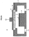
- FIGS. 2A and 2B schematically show the construction a microwave plasma substrate processing apparatus 10 used by the inventor of the present invention.
- the microwave plasma substrate processing apparatus 10 includes a processing vessel 11 accommodating therein a stage 12 for holding a substrate W to be processed, wherein the processing vessel 11 is evacuated at evacuation ports 11A and 11B.
- an opening is formed in the processing vessel 11 in correspondence to the substrate W to be processed on the stage 12, wherein the opening is closed by a cover plate 13 of a low loss ceramic such as quartz, alumina, or the like, and there is formed underneath the cover plate 13 a shower plate 14 of low loss ceramic such as quartz, alumina, or the like, so as to face the substrate W to be processed, wherein the shower plate 14 is formed with a large number of nozzle openings communicating with a gas inlet path 14A.
- a cover plate 13 of a low loss ceramic such as quartz, alumina, or the like
- the shower plate 14 and the cover plate 13 form a microwave window, and a microwave antenna 15 such as a radial line slot antenna, horn antenna, or the like, is formed outside the cover plate 13.
- the processing space inside the processing vessel 11 is set to a predetermined processing pressure by evacuating through the evacuation ports 11A and 11B, and an oxidation gas or a nitridation gas is introduced from the shower plate 14 together with an inert gas such as argon, Kr, or the like.
- Figure 2B is a diagram showing the construction of the radial line slot antenna 15.
- the radial line slot antenna 15 includes a flat, disk-like antenna main body connected to an external microwave source via a coaxial waveguide, or the like, wherein there is provided a radiation plate 15A at the mouth of the antenna main body such that the radiation plate 15A is formed with a large number of slots 15a and a large number of slots 15b intersecting perpendicularly thereto as shown in Figure 2B. Further, a retardation plate (not shown) of dielectric plate of constant thickness is interposed between the between the antenna main body and the radiation plate 15A.
- the processing vessel 11 by introducing a microwave of several GHz from the antenna 15, high density microwave plasma is excited in the processing vessel 11 at the surface of the substrate W to be processed.
- the plasma By exciting the plasma with microwave, the plasma has a low electron temperature with the substrate processing apparatus of Figure 1, and it is possible to avoid damaging of the substrate W to be processed or the inner wall of the processing vessel 11.
- the radicals thus formed are caused to flow along the surface of the substrate W to be processed and are evacuated promptly, and thus, recombination of the radicals is suppressed, and it becomes possible to achieve highly uniform substrate processing efficiently at a low temperature of 550°C or less.
- Figures 3A - 3C are diagrams showing the substrate processing conducted by the inventor of the present invention in the investigation constituting the foundation of the present invention and corresponding to a first embodiment of the present invention, while using substrate processing apparatus 10 of Figure 1.
- a silicon substrate 21, from which the native oxide film is removed by HF treatment is introduced to the processing vessel 11 of the substrate processing apparatus 10 as the substrate W to be processed, and a mixed gas of argon and hydrogen is introduced from the shower plate 14. Further, plasma is formed by exciting the mixed gas by a microwave.
- the process pressure inside the processing vessel 11 is set to 7Pa, and an argon gas and a hydrogen gas are supplied with respective flow rates 1000SCCM and 40SCCM. Further, a microwave of 2.4GHz in frequency is supplied to the microwave antenna 15 with the power of 1500W at the substrate temperature of 400°C, and high density plasma is formed in the vicinity of the surface of the substrate W to be processed.
- an organic substance remaining on the substrate surface is removed effectively in the form of hydrocarbons as a result of exposing the surface of the silicon substrate 21 to the plasma thus formed, even at a low substrate temperature of 400°C, and a fresh silicon surface is exposed at the substrate surface.
- a silicon oxide film 22 is formed on the silicon substrate 21 thus applied with the processing of Figure 3A with the thickness of 10 - 1nm, by setting the processing pressure inside the processing vessel 11 to typically 7Pa and supplying an argon gas and an oxygen gas with respective flow rates of 1000SCCM and 40SCCM, while setting the substrate temperature to 400°C and by supplying the microwave of 2.4GH frequency to the microwave antenna 15 with the power of 1500W.
- Figure 4 shows the relationship between the accumulated defect rate F and the breakdown electric charge amount Qdb (TDDB) for the silicon oxide film thus obtained in comparison with the result of Figure 1. Further, Figure 4 also shows the result for the case in which the silicon substrate 21 is exposed to the argon plasma in the step of Figure 3A. In Figure 4, the silicon oxide film is formed to the thickness of 10nm.
- TDDB breakdown electric charge amount
- the absolute value of the breakdown electric charge amount Qbd of the plasma oxide film of the present embodiment is increased further as compared with the case of thermal oxide film, indicating that the lifetime of the obtained plasma oxide film is increased.
- Figure 5 shows the leakage current characteristics of the silicon oxide film 22 thus formed with the film thickness of 10nm, wherein the measurement of Figure 5 is conducted under the condition of applying a voltage of 12V, and thus, the values are different from the case explained previously in which the measurement was made by applying a voltage of 1V.
- silicon oxide film has been made in the present embodiment on the surface of the silicon substrate 21 in the step of Figure 3B by the mixed gas plasma of argon and hydrogen
- a silicon nitride film 23 by using argon and nitrogen, or argon and ammonia, or argon and a mixed gas of nitrogen and hydrogen.
- a silicon oxynitride film 24 by using argon and nitrogen and oxygen, or argon and ammonia and oxygen, or argon and a mixed gas of nitrogen and hydrogen and oxygen.
- inert gas of other rare gas such as helium, krypton and xenon
- argon an inert gas of other rare gas such as helium, krypton and xenon
- oxidizing gas or nitriding gas such as NO, N 2 O, H 2 O, or the like in the present invention, in place of the oxygen gas, nitrogen gas and ammonia gas.
- Figures 6A and 6B show the substrate processing method according to a second embodiment of the present invention.
- FIG. 6A there is formed a silicon oxide film 22 on a silicon substrate 21 by the process of Figures 3A and 3B explained before or by other process, wherein the surface of the silicon oxide film 22 is processed by the mixture gas plasma of argon and hydrogen under the condition similar to the process of Figure 3A, and the organic substance remaining on the surface of the silicon oxide film 22 is removed.
- the oxide film 25 thus formed has excellent reliability and leakage current density similarly to the plasma oxide film that explained with the previous embodiment.
- a silicon oxynitride film 26 by nitriding the silicon oxide film 22 by using argon and nitrogen, or argon and ammonia, or the mixed gas plasma of argon and nitrogen and hydrogen.
- the present invention is not limited to such a particular substrate processing apparatus, but is effective also in a parallel plate plasma processing apparatus, an ICP plasma processing apparatuses, an ECR plasma processing apparatus, and the like.
Landscapes
- Formation Of Insulating Films (AREA)
- Insulated Gate Type Field-Effect Transistor (AREA)
- Drying Of Semiconductors (AREA)
Abstract
A substrate processing method includes a first step of exposing a silicon substrate surface to mixed gas plasma of an inert gas and hydrogen, and a second step of conducting any of oxidation processing, nitridation processing and oxynitridation processing to said silicon substrate surface by plasma processing after said first step, wherein an organic substance remaining on said substrate surface is removed in said first step. <IMAGE> <IMAGE>
Description
The present invention generally relates to
substrate processing technology, and more
particularly to a substrate processing method for
forming an insulation film on a silicon substrate.
In semiconductor production technology,
formation of insulation film on a silicon substrate
is most fundamental and yet important technology.
Especially, a very high quality insulation film is
required for the gate insulation film, or the like,
of MOS transistors. Meanwhile, the film thickness of
the gate insulation film has been decreased to about
1nm with device miniaturization with recent ultra-miniaturized
high-speed semiconductor devices, and
there is a need for the technology capable of forming
such a thin insulation film with high quality.
Conventionally, high quality silicon oxide
films used for the gate insulation film of a MOS
transistor have been formed by thermal oxidation
processing of a silicon substrate surface. A thermal
oxide film of silicon thus formed has the feature of
small number of dangling bonds, and there is caused
little trapping of carriers even in the case the film
is used for an insulation film covering the channel
region and thus used in the environment in which the
film is subjected to high electric field. Thereby,
stable threshold characteristics are realized.
On the other hand, with the progress in the
miniaturization technology, it is now becoming
possible these days to produce ultra-miniaturized
semiconductor devices having a gate length of 0.1µm
or less.
In order to improve the operational speed
of semiconductor device with such ultra miniaturized
semiconductor devices by way of reducing the gate
length, there is a need of reducing the thickness of
the gate insulation film in accordance with scaling
law. In the case of a MOS transistor having the gate
length of 0,1µm, for example, there is a need of
reducing the thickness of the gate insulation film to
2nm or less. On the other hand, when the film
thickness is decreased like this with a conventional
thermal oxide film, there occurs an increase of gate
leakage current in the form of tunneling current.
From this reason, it has been thought that film
thickness of 2nm would be the limit of gate
insulation film formed by a thermal oxide film. With
a thermal oxide film having the film thickness of 2nm,
a gate leakage current of 1×10⁻²A/cm2 has been
realized.
Contrary to this, there is proposed a
technology capable of forming a higher quality
silicon oxide film by conducting oxidation processing
to a silicon substrate, by using microwave plasma.
With the silicon oxide film thus formed by
microwave plasma oxidation of silicon substrate, it
has been confirmed that leakage current of 1×10⁻²A/cm2
is possible with the application voltage of 1V, even
in the case the film has a film thickness of 1.5nm.
Thus, it is expected that the silicon oxide film
formed by microwave plasma enables breaking through
of the foregoing limit of device miniaturization
encountered in the conventional semiconductor devices
that use a conventional thermal oxide film. Further,
with the substrate processing that uses the microwave
plasma, it becomes possible to form an oxynitride
film or nitride having a large specific dielectric
constant on a silicon substrate with the film quality
exceeding the film quality of a thermal oxide film.
In the case of using an oxynitride film for gate
insulation film, a leakage current of 1×10⁻²A/cm2 or
less is realized at the application voltage of 1V for
an oxynitride film having a film thickness equivalent
to the film thickness of 1nm of silicon oxide film.
Substrate processing by microwave plasma
can be performed at a low temperature typically below
500°C, and because of this, it becomes possible to
reduce the time needed for raising and lowering the
substrate temperature. Thereby, it becomes possible
to produce the semiconductor device with large
throughput. Further, with such low temperature
processing, there occurs no change of impurity
concentration profile of diffusion regions even when
the diffusion regions are already formed in the
substrate, and it becomes possible to realize desired
device characteristics with reliability.
Meanwhile, a gate insulation film is
required to provide the feature of small leakage
current and high reliability.
Figure 1 shows the relationship between the
accumulated defect rate F and integral electric
charge amount (Qbd) leading to breakdown (TDDB
characteristic) for a silicon oxide film formed on a
silicon substrate surface with the thickness of 10nm
by a microwave plasma oxidation processing conducted
by the inventor of the present invention (shown in
the drawing as "plasma oxide film"), in comparison
with a thermal oxide film of the same thickness,
wherein the vertical axis represents the accumulated
defect rate F while the horizontal axis represents
the integral electric charge amount Qbd that leads to
insulation breakdown. It should be noted that the
plasma oxide film has been formed by using a
microwave plasma substrate processing apparatus to be
explained later with Figure 2, by oxidizing the
silicon substrate surface already applied with
removal process of native oxide film in the mixed gas
plasma of argon and oxygen at the substrate
temperature of 400°C.
Referring to Figure 1, the line
representing the accumulated defect rate F forms a
steep gradient with regard to the integral electric
charge amount Qdb in the case of the thermal oxide
film, and thus, insulation breakdown occurs when the
integral electric charge amount Qdb has reached a
predetermined value. Such an insulation film has
excellent reliability characterized predictable
lifetime.
In the case of the plasma oxide film, on
the other hand, the slope of the line representing
the accumulated defect rate F is small, indicating
that breakdown of the insulation film occurs with
various values of the integrated electric charge
amount. With such an insulation film, it is not
possible to predict the device lifetime with
certainty and no reliability is attained for the
semiconductor device.
Accordingly, it is a general object of the
present invention to provide a novel and useful
substrate processing method wherein the foregoing
problems are eliminated.
Another and more specific object of the
present invention is to provide a substrate
processing method capable of forming an oxide film, a
nitride film, or an oxynitride film on a silicon
substrate surface by oxidation processing,
nitridation processing or oxynitridation processing
conducted in plasma with improved reliability and
thus capable of assuring long device lifetime with
the semiconductor device that uses such an insulation
film.
Another object of the present invention is
to provide a substrate processing method, comprising:
According to the present invention, organic
substance remaining on the substrate surface, is
removed effectively by exposing the silicon substrate
surface to the mixture gas plasma of the inert gas
and the hydrogen gas before the substrate processing
by plasma, and it becomes possible to form a very
high-quality insulation film on a fresh silicon
surface.
Other objects and further features of the
present invention will become apparent from the
detailed explanation of invention hereinafter when
read in conjunction with the attached drawings.
The inventor of the present invention has
acquired the knowledge, in an experimental
investigation on the formation process of oxide films,
nitride films and oxynitride films on a silicon
substrate by microwave plasma processing, suggesting
that organic substance remaining on the silicon
substrate surface exerts a significant effect on the
reliability of insulation film formed on the
substrate.
Figures 2A and 2B schematically show the
construction a microwave plasma substrate processing
apparatus 10 used by the inventor of the present
invention.
Referring to Figure 2A, the microwave
plasma substrate processing apparatus 10 includes a
processing vessel 11 accommodating therein a stage 12
for holding a substrate W to be processed, wherein
the processing vessel 11 is evacuated at evacuation
ports 11A and 11B.
Further, an opening is formed in the
processing vessel 11 in correspondence to the
substrate W to be processed on the stage 12, wherein
the opening is closed by a cover plate 13 of a low
loss ceramic such as quartz, alumina, or the like,
and there is formed underneath the cover plate 13 a
shower plate 14 of low loss ceramic such as quartz,
alumina, or the like, so as to face the substrate W
to be processed, wherein the shower plate 14 is
formed with a large number of nozzle openings
communicating with a gas inlet path 14A.
The shower plate 14 and the cover plate 13
form a microwave window, and a microwave antenna 15
such as a radial line slot antenna, horn antenna, or
the like, is formed outside the cover plate 13.
In operation, the processing space inside
the processing vessel 11 is set to a predetermined
processing pressure by evacuating through the
evacuation ports 11A and 11B, and an oxidation gas or
a nitridation gas is introduced from the shower plate
14 together with an inert gas such as argon, Kr, or
the like.
Figure 2B is a diagram showing the
construction of the radial line slot antenna 15.
Referring to Figure 2B, the radial line
slot antenna 15 includes a flat, disk-like antenna
main body connected to an external microwave source
via a coaxial waveguide, or the like, wherein there
is provided a radiation plate 15A at the mouth of the
antenna main body such that the radiation plate 15A
is formed with a large number of slots 15a and a
large number of slots 15b intersecting
perpendicularly thereto as shown in Figure 2B.
Further, a retardation plate (not shown) of
dielectric plate of constant thickness is interposed
between the between the antenna main body and the
radiation plate 15A.
Further, by introducing a microwave of
several GHz from the antenna 15, high density
microwave plasma is excited in the processing vessel
11 at the surface of the substrate W to be processed.
By exciting the plasma with microwave, the plasma has
a low electron temperature with the substrate
processing apparatus of Figure 1, and it is possible
to avoid damaging of the substrate W to be processed
or the inner wall of the processing vessel 11.
Further, the radicals thus formed are caused to flow
along the surface of the substrate W to be processed
and are evacuated promptly, and thus, recombination
of the radicals is suppressed, and it becomes
possible to achieve highly uniform substrate
processing efficiently at a low temperature of 550°C
or less.
Figures 3A - 3C are diagrams showing the
substrate processing conducted by the inventor of the
present invention in the investigation constituting
the foundation of the present invention and
corresponding to a first embodiment of the present
invention, while using substrate processing apparatus
10 of Figure 1.
Referring to Figure 3A, a silicon substrate
21, from which the native oxide film is removed by HF
treatment, is introduced to the processing vessel 11
of the substrate processing apparatus 10 as the
substrate W to be processed, and a mixed gas of argon
and hydrogen is introduced from the shower plate 14.
Further, plasma is formed by exciting the mixed gas
by a microwave.
In an example, the process pressure inside
the processing vessel 11 is set to 7Pa, and an argon
gas and a hydrogen gas are supplied with respective
flow rates 1000SCCM and 40SCCM. Further, a microwave
of 2.4GHz in frequency is supplied to the microwave
antenna 15 with the power of 1500W at the substrate
temperature of 400°C, and high density plasma is
formed in the vicinity of the surface of the
substrate W to be processed.
With the step of Figure 3A, an organic
substance remaining on the substrate surface is
removed effectively in the form of hydrocarbons as a
result of exposing the surface of the silicon
substrate 21 to the plasma thus formed, even at a low
substrate temperature of 400°C, and a fresh silicon
surface is exposed at the substrate surface.
Next, in the step of Figure 3B, a silicon
oxide film 22 is formed on the silicon substrate 21
thus applied with the processing of Figure 3A with
the thickness of 10 - 1nm, by setting the processing
pressure inside the processing vessel 11 to typically
7Pa and supplying an argon gas and an oxygen gas with
respective flow rates of 1000SCCM and 40SCCM, while
setting the substrate temperature to 400°C and by
supplying the microwave of 2.4GH frequency to the
microwave antenna 15 with the power of 1500W.
Figure 4 shows the relationship between the
accumulated defect rate F and the breakdown electric
charge amount Qdb (TDDB) for the silicon oxide film
thus obtained in comparison with the result of Figure
1. Further, Figure 4 also shows the result for the
case in which the silicon substrate 21 is exposed to
the argon plasma in the step of Figure 3A. In Figure
4, the silicon oxide film is formed to the thickness
of 10nm.
Referring to Figure 4, it should be noted
that the process in which the pre-processing of
Figure 3A is omitted, and thus, the silicon oxide
film 22 is formed on the silicon substrate 21
directly with the thickness of 10nm, corresponds to
the plasma oxide film explained previously with
reference to Figure 1, wherein it will be noted that
there appears a large variation of breakdown electric
charge amount Qdb as explained already with reference
to Figure 1.
Contrary to this, in the case the argon
plasma processing is conducted in the pre-processing
step of Figure 3A, it can be seen that variation of
the breakdown electric charge amount Qdb is decreased.
Particularly, in the case the pre pre-processing is
conducted in the mixed gas plasma of argon and
hydrogen as shown in Figure 3A, the variation of the
breakdown electric charge mount Qdb is decreased
further, and a result comparable to the case of a
thermal oxide film is attained. Thus, by carrying out
the pre-processing process of Figure 3A in the
mixture gas plasma of argon and hydrogen, it can be
seen that a plasma oxide film having the reliability
comparable to that of a thermal oxide film is
obtained.
Moreover, as can be seen from Figure 4, the
absolute value of the breakdown electric charge
amount Qbd of the plasma oxide film of the present
embodiment is increased further as compared with the
case of thermal oxide film, indicating that the
lifetime of the obtained plasma oxide film is
increased.
The fact shown in Figures 1 and 4 that the
variation of the breakdown electric charge amount Qbd
is small in the thermal oxide film formed in the
oxidizing ambient at high temperatures and that the
breakdown electric charge amount Qbd is large in the
plasma oxide film formed at the low temperature of
about 400°C, suggests that this phenomenon is related
to organic substances remaining on the surface of the
silicon substrate 21. In the present embodiment, it
is thought that, as a result of the processing of the
surface of the silicon substrate 21 in the mixed gas
plasma of argon and hydrogen in the step of Figure 3A,
the organic substance remaining on the silicon
substrate surface is removed therefrom in the form of
hydrocarbons, and a fresh silicon surface is exposed
at the silicon substrate at the commencement of the
step of Figure 3B.
Figure 5 shows the leakage current
characteristics of the silicon oxide film 22 thus
formed with the film thickness of 10nm, wherein the
measurement of Figure 5 is conducted under the
condition of applying a voltage of 12V, and thus, the
values are different from the case explained
previously in which the measurement was made by
applying a voltage of 1V.
Referring to Figure 5, with the plasma
oxide film shown in Figure 1 in which the pre-processing
step of Figure 3A is omitted, a leakage
current density comparable with that of a
conventional thermal oxide film is obtained, while in
the case in which the plasma pre-processing by argon
gas is conducted in the step of Figure 3A, there is
caused a decrease of leakage current, particularly in
the case the pre-processing process of Figure 3A is
conducted in the mixed gas plasma of argon and
hydrogen.
Further, while formation of silicon oxide
film has been made in the present embodiment on the
surface of the silicon substrate 21 in the step of
Figure 3B by the mixed gas plasma of argon and
hydrogen, it is also possible to form a silicon
nitride film 23 by using argon and nitrogen, or argon
and ammonia, or argon and a mixed gas of nitrogen and
hydrogen. Further, it is also possible to form a
silicon oxynitride film 24 by using argon and
nitrogen and oxygen, or argon and ammonia and oxygen,
or argon and a mixed gas of nitrogen and hydrogen and
oxygen.
Further, it is also possible to use an
inert gas of other rare gas such as helium, krypton
and xenon, in place of argon with the present
embodiment.
Further, it is possible with the present
embodiment to use other oxidizing gas or nitriding
gas such as NO, N2O, H2O, or the like in the present
invention, in place of the oxygen gas, nitrogen gas
and ammonia gas.
Figures 6A and 6B show the substrate
processing method according to a second embodiment of
the present invention.
Referring to Figure 6A, there is formed a
silicon oxide film 22 on a silicon substrate 21 by
the process of Figures 3A and 3B explained before or
by other process, wherein the surface of the silicon
oxide film 22 is processed by the mixture gas plasma
of argon and hydrogen under the condition similar to
the process of Figure 3A, and the organic substance
remaining on the surface of the silicon oxide film 22
is removed.
Next, in the step of Figure 6B, there is
caused a growth of the oxide film on the silicon
oxide film 22 thus processed by applying the mixed
gas plasma of argon and oxygen under the similar
condition as Figure 3B, and with this, there is
formed an oxide film 25.
It should be noted that the oxide film 25
thus formed has excellent reliability and leakage
current density similarly to the plasma oxide film
that explained with the previous embodiment.
Further, in the process of Figure 6B, it is
possible to form a silicon oxynitride film 26 by
nitriding the silicon oxide film 22 by using argon
and nitrogen, or argon and ammonia, or the mixed gas
plasma of argon and nitrogen and hydrogen.
Further, while explanation has been made
for the present embodiment for the case of using the
microwave plasma substrate processing apparatus of
Figures 2A and 2B that uses the radial line slot
antenna 15, it is also possible to omit the shower
plate 14 in the construction of Figure 2A and
introduce the gases from the gas inlet part 14A
directly into the processing vessel 11. Further, the
present invention is not limited to such a particular
substrate processing apparatus, but is effective also
in a parallel plate plasma processing apparatus, an
ICP plasma processing apparatuses, an ECR plasma
processing apparatus, and the like.
Further, while the present invention has
been explained heretofore with regard to preferred
embodiments, the present invention is not limited to
such a particular embodiment but various variations
and modifications may be made within the subject
matter recited in claims.
Claims (10)
- A substrate processing method, comprising:a first step of exposing a silicon substrate surface to mixed gas plasma of an inert gas and hydrogen; anda second step of conducting any of oxidation processing, nitridation processing and oxynitridation processing to said silicon substrate surface by plasma processing after said first step.
- The substrate processing method as claimed in claim 1, wherein said inert gas is a rare gas.
- The substrate processing method as claimed in claim 1, wherein said inert gas comprises any of krypton and xenon.
- The substrate processing method as claimed in claim 1, wherein said firs step and said second step are conducted consecutively in the same plasma processing apparatus .
- The substrate processing method as claimed in claim 1, wherein said mixed gas plasma of said inert gas and hydrogen is excited in said first step by a microwave.
- The substrate processing method as claimed in claim 1, wherein, in said second step, said plasma processing is conducted by using plasma excited by a microwave.
- The substrate processing method as claimed in claim 1, wherein said plasma is excited by a microwave emitted from a radial line slot antenna.
- The substrate processing method as claimed in claim 1, wherein, in said first step, a silicon surface is exposed at a surface of said silicon substrate.
- The substrate processing method as claimed in claim 1, wherein, in said first step, there is formed an insulation film on a surface of said silicon substrate.
- The substrate processing method as claimed in claim 9, wherein said insulation film comprises a silicon oxide film.
Applications Claiming Priority (3)
| Application Number | Priority Date | Filing Date | Title |
|---|---|---|---|
| JP2003054242 | 2003-02-28 | ||
| JP2003054242A JP2004266075A (en) | 2003-02-28 | 2003-02-28 | Substrate processing method |
| PCT/JP2004/002013 WO2004077542A1 (en) | 2003-02-28 | 2004-02-20 | Substrate processing method |
Publications (2)
| Publication Number | Publication Date |
|---|---|
| EP1598859A1 true EP1598859A1 (en) | 2005-11-23 |
| EP1598859A4 EP1598859A4 (en) | 2010-04-28 |
Family
ID=32923455
Family Applications (1)
| Application Number | Title | Priority Date | Filing Date |
|---|---|---|---|
| EP04713215A Withdrawn EP1598859A4 (en) | 2003-02-28 | 2004-02-20 | PROCESS FOR TREATING SUBSTRATES |
Country Status (7)
| Country | Link |
|---|---|
| US (1) | US20060024864A1 (en) |
| EP (1) | EP1598859A4 (en) |
| JP (1) | JP2004266075A (en) |
| KR (1) | KR100800638B1 (en) |
| CN (1) | CN100514573C (en) |
| TW (1) | TWI243424B (en) |
| WO (1) | WO2004077542A1 (en) |
Cited By (2)
| Publication number | Priority date | Publication date | Assignee | Title |
|---|---|---|---|---|
| EP2091074A1 (en) * | 2008-02-13 | 2009-08-19 | S.O.I. TEC Silicon | Method for preparing hydrophobic surfaces |
| WO2009150503A1 (en) * | 2008-06-10 | 2009-12-17 | S.O.I. Tec Silicon On Insulator Technologies | Method for preparing hydrophobic surfaces |
Families Citing this family (11)
| Publication number | Priority date | Publication date | Assignee | Title |
|---|---|---|---|---|
| TW200511430A (en) * | 2003-05-29 | 2005-03-16 | Tokyo Electron Ltd | Plasma processing apparatus and plasma processing method |
| JP4509864B2 (en) * | 2005-05-30 | 2010-07-21 | 東京エレクトロン株式会社 | Plasma processing method and plasma processing apparatus |
| KR20110057645A (en) * | 2009-11-24 | 2011-06-01 | 삼성전자주식회사 | An insulating film forming method and a transistor forming method including the same |
| FR2964112B1 (en) * | 2010-08-31 | 2013-07-19 | Commissariat Energie Atomique | TREATMENT BEFORE BONDING A CU-OXIDE MIXED SURFACE BY PLASMA CONTAINING NITROGEN AND HYDROGEN |
| CN102468170A (en) * | 2010-11-05 | 2012-05-23 | 中芯国际集成电路制造(上海)有限公司 | Forming method of stress layer for improving NFET performance |
| CN104701261B (en) * | 2013-12-04 | 2018-09-07 | 中芯国际集成电路制造(上海)有限公司 | The forming method of transistor |
| CN104550133B (en) * | 2014-12-11 | 2017-02-22 | 河北同光晶体有限公司 | Method for removing organic pollutants in hollow micro-defect and on surface of wafer of silicon carbide single crystal |
| CN109065447B (en) * | 2018-08-03 | 2021-02-26 | 北京中兆龙芯软件科技有限公司 | A power device chip and its manufacturing method |
| KR102225956B1 (en) * | 2018-10-19 | 2021-03-12 | 세메스 주식회사 | Apparatus and method for bonding die and substrate |
| JP7301727B2 (en) * | 2019-12-05 | 2023-07-03 | 東京エレクトロン株式会社 | Plasma processing apparatus and plasma processing method |
| JP7222946B2 (en) * | 2020-03-24 | 2023-02-15 | 株式会社Kokusai Electric | Semiconductor device manufacturing method, substrate processing apparatus, and program |
Family Cites Families (14)
| Publication number | Priority date | Publication date | Assignee | Title |
|---|---|---|---|---|
| JPS6029296B2 (en) * | 1980-03-03 | 1985-07-10 | 舜平 山崎 | Film formation method |
| JPH01198482A (en) * | 1988-02-01 | 1989-08-10 | Canon Inc | Formation of deposited film by microwave plasma cvd |
| JPH01198481A (en) * | 1988-02-01 | 1989-08-10 | Canon Inc | Formation of deposited film by microwave plasma cvd |
| US7053002B2 (en) * | 1998-12-04 | 2006-05-30 | Applied Materials, Inc | Plasma preclean with argon, helium, and hydrogen gases |
| JP3326718B2 (en) * | 1999-03-19 | 2002-09-24 | 富士通株式会社 | Method for manufacturing semiconductor device |
| US6348420B1 (en) * | 1999-12-23 | 2002-02-19 | Asm America, Inc. | Situ dielectric stacks |
| TW520453B (en) * | 1999-12-27 | 2003-02-11 | Seiko Epson Corp | A method to fabricate thin insulating films |
| US6225169B1 (en) * | 2000-02-24 | 2001-05-01 | Novellus Systems, Inc. | High density plasma nitridation as diffusion barrier and interface defect densities reduction for gate dielectric |
| KR20020002732A (en) * | 2000-06-30 | 2002-01-10 | 박종섭 | Method for forming an insulation layer of a semiconductor device |
| JP5068402B2 (en) * | 2000-12-28 | 2012-11-07 | 公益財団法人国際科学振興財団 | Dielectric film and method for forming the same, semiconductor device, nonvolatile semiconductor memory device, and method for manufacturing semiconductor device |
| CN101399198A (en) * | 2001-01-22 | 2009-04-01 | 东京毅力科创株式会社 | Method of manufacturing electronic device material |
| EP1361606B1 (en) * | 2001-01-25 | 2010-11-24 | Tokyo Electron Limited | Method of producing electronic device material |
| JP2003037105A (en) * | 2001-07-26 | 2003-02-07 | Tokyo Electron Ltd | Plasma processing apparatus and method |
| JP4001498B2 (en) * | 2002-03-29 | 2007-10-31 | 東京エレクトロン株式会社 | Insulating film forming method and insulating film forming system |
-
2003
- 2003-02-28 JP JP2003054242A patent/JP2004266075A/en active Pending
-
2004
- 2004-02-17 TW TW093103799A patent/TWI243424B/en not_active IP Right Cessation
- 2004-02-20 WO PCT/JP2004/002013 patent/WO2004077542A1/en not_active Ceased
- 2004-02-20 CN CNB2004800054966A patent/CN100514573C/en not_active Expired - Fee Related
- 2004-02-20 KR KR1020057015979A patent/KR100800638B1/en not_active Expired - Fee Related
- 2004-02-20 EP EP04713215A patent/EP1598859A4/en not_active Withdrawn
-
2005
- 2005-08-26 US US11/211,495 patent/US20060024864A1/en not_active Abandoned
Cited By (2)
| Publication number | Priority date | Publication date | Assignee | Title |
|---|---|---|---|---|
| EP2091074A1 (en) * | 2008-02-13 | 2009-08-19 | S.O.I. TEC Silicon | Method for preparing hydrophobic surfaces |
| WO2009150503A1 (en) * | 2008-06-10 | 2009-12-17 | S.O.I. Tec Silicon On Insulator Technologies | Method for preparing hydrophobic surfaces |
Also Published As
| Publication number | Publication date |
|---|---|
| KR20050104411A (en) | 2005-11-02 |
| CN1757101A (en) | 2006-04-05 |
| WO2004077542A1 (en) | 2004-09-10 |
| US20060024864A1 (en) | 2006-02-02 |
| EP1598859A4 (en) | 2010-04-28 |
| JP2004266075A (en) | 2004-09-24 |
| TWI243424B (en) | 2005-11-11 |
| CN100514573C (en) | 2009-07-15 |
| TW200419672A (en) | 2004-10-01 |
| KR100800638B1 (en) | 2008-02-01 |
Similar Documents
| Publication | Publication Date | Title |
|---|---|---|
| JP4795407B2 (en) | Substrate processing method | |
| US7226874B2 (en) | Substrate processing method | |
| JP4926219B2 (en) | Manufacturing method of electronic device material | |
| US20070204959A1 (en) | Substrate processing method and material for electronic device | |
| CN100429753C (en) | Plasma processing method, semiconductor substrate, and plasma processing apparatus | |
| US20070169696A1 (en) | Two-step post nitridation annealing for lower eot plasma nitrided gate dielectrics | |
| EP1598859A1 (en) | Substrate processing method | |
| JP2008147678A (en) | Material for electronic device and manufacturing method thereof | |
| US20040250771A1 (en) | Microwave plasma substrate processing device | |
| CN101194345B (en) | Plasma nitriding method and apparatus, and semiconductor device manufacturing method | |
| JP2003188172A (en) | Substrate processing method | |
| JP2005235792A (en) | Substrate processing method | |
| US20080242113A1 (en) | Film forming method of high-k dielectric film |
Legal Events
| Date | Code | Title | Description |
|---|---|---|---|
| PUAI | Public reference made under article 153(3) epc to a published international application that has entered the european phase |
Free format text: ORIGINAL CODE: 0009012 |
|
| 17P | Request for examination filed |
Effective date: 20050826 |
|
| AK | Designated contracting states |
Kind code of ref document: A1 Designated state(s): AT BE BG CH CY CZ DE DK EE ES FI FR GB GR HU IE IT LI LU MC NL PT RO SE SI SK TR |
|
| AX | Request for extension of the european patent |
Extension state: AL LT LV MK |
|
| DAX | Request for extension of the european patent (deleted) | ||
| RBV | Designated contracting states (corrected) |
Designated state(s): DE FR GB IT NL |
|
| A4 | Supplementary search report drawn up and despatched |
Effective date: 20100331 |
|
| STAA | Information on the status of an ep patent application or granted ep patent |
Free format text: STATUS: THE APPLICATION HAS BEEN WITHDRAWN |
|
| 18W | Application withdrawn |
Effective date: 20100707 |