EP1598848A2 - Electron microscope - Google Patents
Electron microscope Download PDFInfo
- Publication number
- EP1598848A2 EP1598848A2 EP05253138A EP05253138A EP1598848A2 EP 1598848 A2 EP1598848 A2 EP 1598848A2 EP 05253138 A EP05253138 A EP 05253138A EP 05253138 A EP05253138 A EP 05253138A EP 1598848 A2 EP1598848 A2 EP 1598848A2
- Authority
- EP
- European Patent Office
- Prior art keywords
- specimen
- magnetic
- microprobe
- image
- electron microscope
- Prior art date
- Legal status (The legal status is an assumption and is not a legal conclusion. Google has not performed a legal analysis and makes no representation as to the accuracy of the status listed.)
- Granted
Links
Images



Classifications
-
- H—ELECTRICITY
- H01—ELECTRIC ELEMENTS
- H01J—ELECTRIC DISCHARGE TUBES OR DISCHARGE LAMPS
- H01J37/00—Discharge tubes with provision for introducing objects or material to be exposed to the discharge, e.g. for the purpose of examination or processing thereof
- H01J37/26—Electron or ion microscopes; Electron or ion diffraction tubes
- H01J37/266—Measurement of magnetic or electric fields in the object; Lorentzmicroscopy
- H01J37/268—Measurement of magnetic or electric fields in the object; Lorentzmicroscopy with scanning beams
-
- H—ELECTRICITY
- H01—ELECTRIC ELEMENTS
- H01J—ELECTRIC DISCHARGE TUBES OR DISCHARGE LAMPS
- H01J2237/00—Discharge tubes exposing object to beam, e.g. for analysis treatment, etching, imaging
- H01J2237/15—Means for deflecting or directing discharge
- H01J2237/151—Electrostatic means
- H01J2237/1514—Prisms
-
- H—ELECTRICITY
- H01—ELECTRIC ELEMENTS
- H01J—ELECTRIC DISCHARGE TUBES OR DISCHARGE LAMPS
- H01J2237/00—Discharge tubes exposing object to beam, e.g. for analysis treatment, etching, imaging
- H01J2237/25—Tubes for localised analysis using electron or ion beams
- H01J2237/2505—Tubes for localised analysis using electron or ion beams characterised by their application
- H01J2237/2588—Lorenz microscopy (magnetic field measurement)
Definitions
- the present invention relates to an electron microscope.
- a specimen has been observed by directing an electron beam at the specimen such that the beam is transmitted through the specimen to create a specimen image, magnifying the specimen image by a magnetic lens, and projecting the image onto a screen.
- a technique for inserting a biprism into such a conventional transmission electron microscope is known as described, for example, in Patent Reference 1.
- the biprism creates interference fringes (hologram) by interference between the electron beam passing through a vacuum and the beam transmitted through the specimen. Information about variations in the phase of the beam is taken from the hologram. Information about the thickness distribution across the specimen, the electric field, or the magnetic field is obtained.
- a magnetic field application means is installed between the polepieces of the objective lens of an electron microscope.
- a DC current produced by a magnetic field application power supply or an AC current having an arbitrary phase, period, or amplitude is applied to the magnetic field application means with an arbitrary synchronizing signal to obtain information about magnetic domain structure while observing an electron microscope image of a magnetic material to which a magnetic field is applied (see, for example, Patent Reference 3).
- Fig. 8 illustrates the prior art method of applying a magnetic field to a specimen.
- the specimen indicated by numeral 1
- the specimen is made of a magnetic material and held by a specimen holder 2.
- An excitation coil 3 is used to apply a magnetic field to the specimen 1.
- Indicated by e is an electron beam. Magnetic flux going out of the N pole of the excitation coil 3 enters the exciting coil 3 on the S-pole side. At this time, the magnetic flux 4 produced by the excitation coil 3 for producing a magnetic field penetrates through the specimen 1 of magnetic material, thus applying a magnetic field to the specimen 1.
- the beam e is directed at the specimen 1.
- the magnetic field produced by the excitation coil is applied to the specimen of magnetic material.
- substantially uniform magnetic field is applied to the whole specimen.
- the applied magnetic field is strong (e.g., more than hundreds of gauss)
- the incident electron beam is deflected to a great extent by the magnetic field because the uniform magnetic field is applied over a wide range and over the whole specimen in this way. That is, with the prior art method described above, a strong magnetic field cannot be applied to the specimen of magnetic material. Consequently, imaging under environments of such strong magnetic fields cannot be performed. It would therefore be desirable to provide an electron microscope which is capable of imaging under environments of such strong magnetic fields.
- the invention provides an electron microscope which is equipped with a magnetic microprobe capable of producing a high magnetic flux density per unit area and applying a strong magnetic field to a local area on a specimen of a magnetic material such that an electron beam incident on the specimen is hardly deflected.
- an electron microscope equipped with a magnetic microprobe the microscope creating an image of a specimen made of a magnetic material based on an electron beam transmitted through the specimen, said microscope comprising: a holder for holding said specimen made of the magnetic material; said magnetic microprobe being made of a magnetic material, the microprobe having a needlelike tip; and a moving mechanism capable of moving said microprobe toward and away from said specimen.
- an electron microscope designed to create an image of a specimen made of a magnetic material according to an electron beam transmitted through the specimen.
- the microscope has a holder for holding the specimen, a magnetic microprobe having a needlelike tip and made of a magnetic material, and a moving mechanism capable of moving the microprobe toward and away from the specimen.
- An arbitrary part of the area on the specimen of magnetic material can therefore be magnetized.
- the electron beam incident on the specimen is little deflected by the applied magnetic field. Image data about the part of the area can be obtained.
- the electron microscope is equipped with a biprism for producing interference between an electron beam transmitted through a specimen made of a magnetic material and an electron beam passing through a vacuum.
- Data about an image created by the beam transmitted through the biprism is accepted (received) and subjected to given image processing.
- a holographic image of the specimen is obtained.
- a holographic image of the specimen of magnetic material can be obtained by performing given computational processing such as Fourier transform on the accepted image. Consequently, characteristics of the magnetic material can be analyzed.
- the electron microscope is further characterized in that the image of the specimen is processed to obtain a Lorentz image.
- a Lorentz image can therefore be obtained.
- the magnetic microprobe uses a permanent magnet.
- the permanent magnet can be used as the magnetic microprobe. In consequence, the structure of the magnetic microprobe can be made simpler.
- the magnetic microprobe is equipped with a mechanism that uses an electromagnet to vary the strength of the produced magnetic field.
- the strength of the magnetic field can be adjusted by using the electromagnet as the magnetic microprobe.
- the moving mechanism for varying the strength uses as its power source an electric motor or piezoelectric device.
- the microprobe can then be moved using the motor or piezoelectric device.
- the specimen made of magnetic material is carried on a drive mechanism for driving the specimen in X-, Y-, and Z-directions.
- the magnetic microprobe is carried on a drive mechanism for driving the microprobe in the X-, Y-, and Z-directions.
- the specimen of magnetic material and the magnetic microprobe canbe independently driven in the X-, Y-, and Z-directions. Therefore, the positions of the specimen and microprobe can be varied precisely.
- Fig. 1 shows an example of structure of a microprobe according to a first embodiment of the present invention.
- This microprobe has a specimen holder 12.
- Fig. 1 is a top view as taken from above the holder.
- a specimen 11 made of a magnetic material is held to the holder 12.
- a magnetic microprobe (hereinafter may be referred to as the probe) 13 is made of a magnetic material and has a needlelike tip.
- the probe 13 is made of a permanent magnet.
- the diameter of the tip of the probe 13 is about 1 ⁇ m. Any technique for reducing the diameter of the tip of the probe 13 down to about 1 ⁇ m involves great difficulties but we have developed a technique for fabricating such a probe.
- the probe 13 is held by a probe-holding portion 15, which in turn is held to a specimen stage 14 capable of moving in the direction indicated by the arrows. That is, the stage 14 can move toward and away from the specimen.
- a specimen stage 14 capable of moving in the direction indicated by the arrows. That is, the stage 14 can move toward and away from the specimen.
- the specimen 11 made of magnetic material is held to the specimen holder 12 as described previously.
- the probe 13 is moved and brought to a stop in an arbitrary position on the specimen 11. Since the tip of the microprobe 13 is sharp, the magnetic flux density is quite high.
- the portion of the specimen 11 over which the probe 13 rests is magnetized by bringing the probe 13 having such magnetic flux density into an arbitrary position over the specimen 11.
- an electrically operated drive mechanism such as a stepping motor or piezoelectric device
- the driving force of the drive mechanism can be controlled from the outside.
- the illustrated mechanism is totally inserted in the specimen chamber of an electron microscope (not shown).
- the specimen 11 of magnetic material and the probe 13 are observed as electron microscope images at the same time.
- Lorentz microscopy is used, magnetic domains and domain walls of the specimen 11 and probe 13 are observed.
- the distribution of magnetic flux can be observed on its reconstructed image if electron holography is used.
- the mechanism for driving the probe 13 is controlled from the outside of the microscope to move the probe toward or away from the specimen 11.
- an arbitrary part of the specimen 11 of magnetic material can be magnetized and image data about this part can be obtained. Furthermore, the structure of the probe can be simplified by using a permanent magnet as the probe.
- the specimen stage 14 can be driven to move the probe 13 toward or away from the specimen 11 of magnetic material as described previously.
- a stepping motor or piezoelectric device is used as the mechanism for driving the stage 14. In this case, movement of the probe 13 can be easily controlled from the outside.
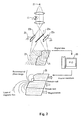
- Fig. 2 shows an example of configuration of an electron microscope according to one embodiment of the present invention.
- This microscope consists of a transmission electron microscope and is operated to display a hologram.
- Like components are indicated by like reference numerals in both Figs. 1 and 2.
- a field emission gun 21 emits an electron beam at a specimen 11 made of a magnetic material.
- the magnetic microprobe 13 as shown in Fig. 1 can be brought close to the specimen 11. As a result, a part of the area on the specimen 11 is magnetized by the probe 13. The specimen 11 magnetized in this way is irradiated with the electron beam.
- a transmission image created by the electron beam is focused by the objective lens and then enters a biprism 22.
- the biprism 22 produces interference between electron beam (reference wave) passing through a vacuum and electron beam (object wave) transmitted through the specimen, forming interference fringes.
- the biprism 22 includes a conductive wire 22a including a mechanism permitting either application of an electric field or grounding.
- Grounding electrodes 22b and 22c are disposed parallel to the conductive wire 22a and on the opposite sides of the wire 22a. The grounding electrodes 22b and 22c act to tailor the electric field produced across the conductive wire 22a. The operation of the instrument constructed in this way is described below.
- an imaging process based on digital computational analysis of electron holography is obtained.
- the analysis based on the electron holography consists of two imaging steps including a first step consisting of creating a hologram by the use of the biprism 22.
- Object wave TEM image of the specimen
- TEM image of the specimen obtained by passage of a transmission electron beam through the specimen 11 of magnetic material interferes with reference wave passing through a vacuum, resulting in a hologram.
- phase shift of electron waves is extracted from the hologram by Fourier transform andthusaphase-reconstructedimage (holographic image) isobtained.
- the electron beam radiated from the electron gun 21 is accelerated and focused by the condenser lens system.
- the transmission electron beam passed through the specimen is placed in position on a half of the object plane displayed by a collimated electron beam.
- the electron beam passed through the biprism 22 creates an electron hologram 23 at interference fringes 24.
- This electron hologram is converted into an electrical signal by a photoelectric device and then converted into digital data by an A/D converter (not shown).
- the digital data, or image data is input into a personal computer 26.
- the input image data is processed in a given manner, e.g., Fourier-transformed.
- a phase-reconstructed image (holographic image) 25 of the part of the area on the magnetized specimen 11 is obtained. Characteristics of the specimen 11 can be investigated by observing the holographic image 25.
- the right half of the reconstructed image 25 is a holographic image, while the left half is an image not affected by the magnetic field. It can be seen that lines of magnetic force radiate out from the holographic image.
- a holographic image of the specimen of magnetic material can be obtained by performing given processing (such as Fourier transform) on the accepted image. Characteristics of the specimen can be analyzed.
- a specimen holder is used.
- a sharp tip made of a material Nd 2 Fe 14 B is driven using a stepping motor or piezoelectric device and brought close to a specimen of magnetic material.
- the hard magnetic material is magnetized. It is assumed here that the magnetic field produced by the probe tip is almost constant within the limited width of the field on the display screen. In particular, it is approximately 460 nm when the Lorentz objective lens is excited. This is sufficient for analysis utilizing electron holography.
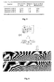
- FIG. 3 shows examples of images obtained by processing by a method according to embodiments of the present invention.
- (a) - (c) show Lorentz microscope images, which are examples of half-tone photographs of the main window displayed on a display screen according to an embodiment of the invention.
- (d) to (f) show reconstructed images (holographic images) of a specimen of magnetic material Nd 2 Fe 14 B, respectively.
- the white and black stripes shown in (a) to (c) show magnetic domain walls of the specimen 11 of magnetic material. The distance between the probe and the specimen is indicated at the right end of each image.
- a Lorentz microscope is now described.
- a case in which a magnetized specimen of magnetic material is irradiated with an electron beam is now discussed. It can be considered that the magnetized specimen is a collection of tiny magnets each consisting of N and S poles. Among these magnets, magnetic flux flows from N to S pole.
- An electron beam is affected by the magnetic field and deflected.
- the space is divided into first spatial parts against which the beam transmitted through the magnets collides and second spatial parts where there is no electron beam.
- the image In the first spatial parts, the image is brighter.
- the second spatial parts the image is darker. Since magnetic domain walls create these brighter and darker portions of the image, Lorentz microscopy can detect magnetic domain walls of a magnetic material.
- the biprism is retracted from the optical axis when a Lorentz image is obtained. An image created by the beam transmitted through the specimen is processed, thus producing a Lorentz image.
- phase images of (d) to (f) showphase images (holographic images) reconstructed in cases where Nd 2 Fe 14 B magnetic substance is used.
- These phase images of (d) to (f) are holographic images created by a method according to one embodiment of the invention.
- the direction of flow of the magnetic flux is indicated by the arrows.
- Each numerical value in the figures indicates the distance between the specimen 11 of magnetic material and probe 13. Characteristics of the specimen can be investigated by obtaining these images.
- the reconstructed phase images indicate that the phases of the magnetic walls (indicated by white and black dots) have been shifted by the magnetic field produced by the probe 13. In these locations, the distance between the probe 13 and the specimen 11 is reduced further.
- Fig. 4 shows a result of an experiment made when a microscopic material of Nd 4.5 Fe 77 B 18.5 was annealed to 983 K. Experiments were performed on the specimen of magnetic material to obtain its magnetic property, which is shown in the table of Fig. 5.
- Fig. 4 shows a holographic image obtained from Nd 4.5 Fe 77 B 18.5 that is a microscopic synthetic after annealing it to 983 K. The distance between the probe and the specimen of magnetic material is shown in the figure. The bold arrow indicates the direction in which the probe approaches the specimen.
- the magnetic flux distribution in the reconstructed phase image varies slightly.
- the density of the lines of magnetic flux is found to be lesser near the specimen edge and the central portion of the image. This may be the result of radiation damage due to ion milling.
- the direction of magnetic flux has the property that as the probe approaches the specimen, the direction of the magnetic flux becomes parallel to the magnetic field as shown in the lower part of Fig. 4(a).
- the sharpened probe produces a magnetic field around the specimen 11 of magnetic material.
- the magnetic field is not yet measured accurately but the magnetic domain walls and magnetic flux are created by the probe made of Nd 2 Fe 14 B.
- a measurement has shown that the probe can be moved in response to the magnetic field produced in the boundary region of the magnetic flux owing to Nd 2 Fe 14 B. This movement is controlled by a stepping motor or piezoelectric device. It seems that a specimen holder having a sharpened probe and a piezoelectric device clarifies the magnetization process of a hard magnetic material.
- a probe having a sharpened tip and made of a permanent magnet of magnetic material Nd 2 Fe 14 B producing a strong magnetic field was fabricated.
- the probe was set in the specimen holder driven by a stepping motor or piezoelectric device.
- An obtained hologram was reconstructed into a phase image by computer processing, resulting in holographic images as shown in (b) and (c).
- (b) and (c) show holographic images of the specimen of magnetic material.
- (b) shows the characteristics of the probe in a case where it is located remotely from the specimen surface of the magnetic material.
- (c) shows the characteristics of the probe in a case where it is located close to the specimen surface.
- the direction in which the probe approaches is indicated by the arrow on top of (b).
- the arrows shown within (b) and (c) indicate the directions of magnetic fluxes.
- Inner and outer magnetic fluxes within the specimen of magnetic material vary gradually as the S pole of the probe approaches the specimen surface. This demonstrates that clarifying the magnetization process using a hard magnetic material by electron holography is quite advantageous. However, the strong magnetic field created by the probe is limited to a restricted area in the specimen.
- the probe is moved by the specimen stage capable of moving the probe toward a specimen of magnetic material.
- the specimen stage to which a specimen of magnetic material is held may be carried on a mechanism capable of moving in the X-, Y-, and Z-directions.
- the probe may be carried on a mechanism capable of moving in the X-, Y-, andZ-directions.
- Fig. 7 shows another example of configuration of a magnetic microprobe using an electromagnet.
- a rod 30 is made of a magnetic material.
- An exciting coil 31 is wound around the rod 30.
- a probe 32 is mounted at one end of the rod 30.
- Indicated by E is a DC voltage source.
- a variable resistor VR is connected with one end of the exciting coil 31.
- the rod 30 of magnetic material and the exciting coil 31 (solenoid coil) cooperate to form a solenoid.
- One end of the DC voltage source E is connected with the exciting coil 31, while the other end is connected with the variable resistor VR. That is, the DC voltage E is applied to the series circuit consisting of the exciting coil 31 and variable resistor VR.
- the shown probe 32 can be moved in the direction indicated by the arrow together with the solenoid. The operation of the probe constructed in this way is described below.
- variable resistor VR is mounted and so the magnitude of the excitation, i.e., the strength of the magnetic field, can be varied by varying the resistance value of the variable resistor.
- the probe shown in Fig. 7 is more complex in structure than the probe shown in Fig. 1 but has the feature that the strength of the magnetic field can be varied. In this way, according to this embodiment, the strength of the magnetic field can be adjusted by using an electromagnet as the magnetic microprobe.
- a probe made of a magnetic material and having a tip of 1-micron size is set into a specimen holder of an electron microscope.
- the distance between a specimen of magnetic material and the probe is made variable. Therefore, a strong magnetic field can be produced in a local area on the specimen. At the same time, the strengthof the field canbe varied. Magnetic characteristics and dynamical variations of the specimen can be observed.
- the present invention can be utilized in fields related to electron microscopy, electron holography microscopy, and Lorentz microscopy.
Landscapes
- Chemical & Material Sciences (AREA)
- Analytical Chemistry (AREA)
- Analysing Materials By The Use Of Radiation (AREA)
- Sampling And Sample Adjustment (AREA)
Abstract
Description
Claims (8)
- An electron microscope for creating an image of a specimen made of a magnetic material based on an electron beam transmitted through the specimen, the microscope comprising:a holder for holding the specimen made of the magnetic material;a magnetic microprobe made of a magnetic material and having a needlelike tip; anda moving mechanism for moving the microprobe toward and away from the specimen.
- An electron microscope equipped with a magnetic microprobe as set forth in claim 1, wherein there is further provided a biprism for producing interference between the electron beam transmitted through said specimen and an electron beam passing through a vacuum, and wherein a holographic image of said specimen is obtained by accepting data about an image created by the electron beam transmitted through said biprism and performing given image processing on the accepted data.
- An electron microscope equipped with a magnetic microprobe as set forth in claim 1, wherein said image of said specimen is processed to obtain a Lorentz image.
- An electron microscope equipped with a magnetic microprobe as set forth in anypreceding claim, wherein said magnetic microprobe uses a permanent magnet.
- An electron microscope equipped with a magnetic microprobe as set forth in any of claims 1 to 3, wherein said magnetic microprobe uses an electromagnet and has a mechanism for varying the strength of a produced magnetic field.
- An electron microscope equipped with a magnetic microprobe as set forth in any preceding claim, wherein said moving mechanism uses as its power source an electric motor or piezoelectric device.
- An electron microscope equipped with a magnetic microprobe as set forth in any preceding claim, wherein said specimen is carried on a drive mechanism for driving the specimen in X-, Y-, and Z-directions.
- An electron microscope equipped with a magnetic microprobe as set forth in any preceding claim, wherein said microprobe is carried on a drive mechanism for driving the microprobe in the X-, Y-, and Z-directions.
Applications Claiming Priority (2)
| Application Number | Priority Date | Filing Date | Title |
|---|---|---|---|
| JP2004152286A JP4323376B2 (en) | 2004-05-21 | 2004-05-21 | Electron microscope with magnetic microprobe |
| JP2004152286 | 2004-05-21 |
Publications (3)
| Publication Number | Publication Date |
|---|---|
| EP1598848A2 true EP1598848A2 (en) | 2005-11-23 |
| EP1598848A3 EP1598848A3 (en) | 2006-11-02 |
| EP1598848B1 EP1598848B1 (en) | 2008-01-16 |
Family
ID=34941405
Family Applications (1)
| Application Number | Title | Priority Date | Filing Date |
|---|---|---|---|
| EP05253138A Expired - Lifetime EP1598848B1 (en) | 2004-05-21 | 2005-05-20 | Electron microscope |
Country Status (4)
| Country | Link |
|---|---|
| US (1) | US7241995B2 (en) |
| EP (1) | EP1598848B1 (en) |
| JP (1) | JP4323376B2 (en) |
| DE (1) | DE602005004328T2 (en) |
Families Citing this family (7)
| Publication number | Priority date | Publication date | Assignee | Title |
|---|---|---|---|---|
| JP4919404B2 (en) * | 2006-06-15 | 2012-04-18 | 株式会社リコー | Electron microscope, electron beam hologram creating method, and phase reproduction image creating method |
| NL2006308C2 (en) * | 2010-03-01 | 2013-05-27 | Zeiss Carl Nts Gmbh | Transmission electron microscope. |
| US20140197312A1 (en) * | 2011-09-30 | 2014-07-17 | Hitachi, Ltd. | Electron microscope and sample observation method |
| KR101672263B1 (en) * | 2015-04-24 | 2016-11-17 | 서울대학교산학협력단 | An electron microscope holder and probe unit therefor |
| JP6718782B2 (en) * | 2016-09-21 | 2020-07-08 | 日本電子株式会社 | Objective lens and transmission electron microscope |
| WO2018139220A1 (en) * | 2017-01-24 | 2018-08-02 | 国立大学法人東北大学 | Method for creating electron-beam hologram, magnetic field information measurement method, and magnetic field information measuring device |
| CN112038039B (en) | 2020-05-27 | 2021-08-24 | 中国科学院宁波材料技术与工程研究所 | A magnetic field generating device and a transmission electron microscope sample rod capable of applying a magnetic field |
Family Cites Families (6)
| Publication number | Priority date | Publication date | Assignee | Title |
|---|---|---|---|---|
| JPH0614458B2 (en) * | 1987-05-28 | 1994-02-23 | 日本電子株式会社 | Magnetic domain observation device |
| US5196701A (en) * | 1991-07-31 | 1993-03-23 | International Business Machines Corporation | High-resolution detection of material property variations |
| JPH0896737A (en) | 1994-09-29 | 1996-04-12 | Hitachi Ltd | electronic microscope |
| JP3276816B2 (en) | 1995-09-12 | 2002-04-22 | 日本電子株式会社 | Electron biprism |
| JP2002117800A (en) * | 2000-10-05 | 2002-04-19 | Jeol Ltd | Electron microscope equipped with an electron biprism device |
| JP4096303B2 (en) * | 2001-12-28 | 2008-06-04 | エスアイアイ・ナノテクノロジー株式会社 | Scanning probe microscope |
-
2004
- 2004-05-21 JP JP2004152286A patent/JP4323376B2/en not_active Expired - Fee Related
-
2005
- 2005-05-20 DE DE602005004328T patent/DE602005004328T2/en not_active Expired - Lifetime
- 2005-05-20 EP EP05253138A patent/EP1598848B1/en not_active Expired - Lifetime
- 2005-05-20 US US11/134,090 patent/US7241995B2/en not_active Expired - Lifetime
Also Published As
| Publication number | Publication date |
|---|---|
| US7241995B2 (en) | 2007-07-10 |
| DE602005004328D1 (en) | 2008-03-06 |
| EP1598848A3 (en) | 2006-11-02 |
| JP4323376B2 (en) | 2009-09-02 |
| US20050274889A1 (en) | 2005-12-15 |
| EP1598848B1 (en) | 2008-01-16 |
| JP2005332772A (en) | 2005-12-02 |
| DE602005004328T2 (en) | 2009-01-15 |
Similar Documents
| Publication | Publication Date | Title |
|---|---|---|
| CN104303256B (en) | Charged Particle Vortex Wave Generation | |
| Chapman | The investigation of magnetic domain structures in thin foils by electron microscopy | |
| US5465046A (en) | Magnetic force microscopy method and apparatus to detect and image currents in integrated circuits | |
| US20230089136A1 (en) | Magnetic field generation device, and transmission electron microscope sample holder capable of applying magnetic field | |
| Tanigaki et al. | Electron holography observation of individual ferrimagnetic lattice planes | |
| US20070216412A1 (en) | Magnetic resonance force microscope | |
| EP1598848B1 (en) | Electron microscope | |
| De Graef | 2. Lorentz microscopy: Theoretical basis and image simulations | |
| Shindo et al. | Material Characterization Using Electron Holography | |
| JP2024025989A (en) | DC magnetic field measurement method and DC magnetic field measurement device, and AC magnetic field measurement method and AC magnetic field measurement device | |
| US11163974B2 (en) | Image acquisition system and image acquisition method | |
| Dooley et al. | Energy filtered Lorentz microscopy | |
| Bai et al. | An in-situ magnetising holder achieving 1.5 T in-plane field in 200 kV transmission electron microscope | |
| JP4397708B2 (en) | Magnetic resonance force microscope and magnetic chip for magnetic resonance force microscope | |
| JP6786121B2 (en) | Electron hologram creation method, magnetic field information measurement method and magnetic field information measurement device | |
| Kohashi et al. | Magnetic-field-application system at high temperatures for spin-polarized scanning-electron-microscopy measurement | |
| Steierl et al. | Surface domain imaging in external magnetic fields | |
| RU2833421C1 (en) | External magnetic field source for magnetic force microscopy | |
| WO2015182564A1 (en) | Evaluation device and evaluation method for magnetic force microscope probe, magnetic force microscope, and method of adjusting magnetic field for control of magnetic force microscope | |
| Celotta et al. | Magnetic Domain Imaging of Spintronic Devices | |
| JPH09270242A (en) | Electron beam equipment | |
| Park et al. | Electron holography on remanent magnetization distribution of melt-spun Nd-Fe-B magnets | |
| Gavrin et al. | SEMPA imaging of domain dynamics in amorphous metals | |
| Lanz et al. | Nondestructive Analysis of Coercivity Distributions in Permanent Magnets with Locally Enhanced Magnetic Properties | |
| Holl | High frequency STM and spin polarized STM on magnetic vortices |
Legal Events
| Date | Code | Title | Description |
|---|---|---|---|
| PUAI | Public reference made under article 153(3) epc to a published international application that has entered the european phase |
Free format text: ORIGINAL CODE: 0009012 |
|
| AK | Designated contracting states |
Kind code of ref document: A2 Designated state(s): AT BE BG CH CY CZ DE DK EE ES FI FR GB GR HU IE IS IT LI LT LU MC NL PL PT RO SE SI SK TR |
|
| AX | Request for extension of the european patent |
Extension state: AL BA HR LV MK YU |
|
| PUAL | Search report despatched |
Free format text: ORIGINAL CODE: 0009013 |
|
| AK | Designated contracting states |
Kind code of ref document: A3 Designated state(s): AT BE BG CH CY CZ DE DK EE ES FI FR GB GR HU IE IS IT LI LT LU MC NL PL PT RO SE SI SK TR |
|
| AX | Request for extension of the european patent |
Extension state: AL BA HR LV MK YU |
|
| 17P | Request for examination filed |
Effective date: 20061227 |
|
| GRAP | Despatch of communication of intention to grant a patent |
Free format text: ORIGINAL CODE: EPIDOSNIGR1 |
|
| AKX | Designation fees paid |
Designated state(s): DE GB |
|
| GRAS | Grant fee paid |
Free format text: ORIGINAL CODE: EPIDOSNIGR3 |
|
| GRAA | (expected) grant |
Free format text: ORIGINAL CODE: 0009210 |
|
| AK | Designated contracting states |
Kind code of ref document: B1 Designated state(s): DE GB |
|
| REG | Reference to a national code |
Ref country code: GB Ref legal event code: FG4D |
|
| REF | Corresponds to: |
Ref document number: 602005004328 Country of ref document: DE Date of ref document: 20080306 Kind code of ref document: P |
|
| PLBE | No opposition filed within time limit |
Free format text: ORIGINAL CODE: 0009261 |
|
| STAA | Information on the status of an ep patent application or granted ep patent |
Free format text: STATUS: NO OPPOSITION FILED WITHIN TIME LIMIT |
|
| 26N | No opposition filed |
Effective date: 20081017 |
|
| PGFP | Annual fee paid to national office [announced via postgrant information from national office to epo] |
Ref country code: GB Payment date: 20220519 Year of fee payment: 18 Ref country code: DE Payment date: 20220519 Year of fee payment: 18 |
|
| REG | Reference to a national code |
Ref country code: DE Ref legal event code: R119 Ref document number: 602005004328 Country of ref document: DE |
|
| GBPC | Gb: european patent ceased through non-payment of renewal fee |
Effective date: 20230520 |
|
| PG25 | Lapsed in a contracting state [announced via postgrant information from national office to epo] |
Ref country code: DE Free format text: LAPSE BECAUSE OF NON-PAYMENT OF DUE FEES Effective date: 20231201 Ref country code: GB Free format text: LAPSE BECAUSE OF NON-PAYMENT OF DUE FEES Effective date: 20230520 |