EP1598443A2 - Superconductivity in boron-doped diamond thin film - Google Patents
Superconductivity in boron-doped diamond thin film Download PDFInfo
- Publication number
- EP1598443A2 EP1598443A2 EP05253160A EP05253160A EP1598443A2 EP 1598443 A2 EP1598443 A2 EP 1598443A2 EP 05253160 A EP05253160 A EP 05253160A EP 05253160 A EP05253160 A EP 05253160A EP 1598443 A2 EP1598443 A2 EP 1598443A2
- Authority
- EP
- European Patent Office
- Prior art keywords
- boron
- thin film
- diamond thin
- doped diamond
- superconductivity
- Prior art date
- Legal status (The legal status is an assumption and is not a legal conclusion. Google has not performed a legal analysis and makes no representation as to the accuracy of the status listed.)
- Granted
Links
Images


Classifications
-
- C—CHEMISTRY; METALLURGY
- C23—COATING METALLIC MATERIAL; COATING MATERIAL WITH METALLIC MATERIAL; CHEMICAL SURFACE TREATMENT; DIFFUSION TREATMENT OF METALLIC MATERIAL; COATING BY VACUUM EVAPORATION, BY SPUTTERING, BY ION IMPLANTATION OR BY CHEMICAL VAPOUR DEPOSITION, IN GENERAL; INHIBITING CORROSION OF METALLIC MATERIAL OR INCRUSTATION IN GENERAL
- C23C—COATING METALLIC MATERIAL; COATING MATERIAL WITH METALLIC MATERIAL; SURFACE TREATMENT OF METALLIC MATERIAL BY DIFFUSION INTO THE SURFACE, BY CHEMICAL CONVERSION OR SUBSTITUTION; COATING BY VACUUM EVAPORATION, BY SPUTTERING, BY ION IMPLANTATION OR BY CHEMICAL VAPOUR DEPOSITION, IN GENERAL
- C23C16/00—Chemical coating by decomposition of gaseous compounds, without leaving reaction products of surface material in the coating, i.e. chemical vapour deposition [CVD] processes
- C23C16/22—Chemical coating by decomposition of gaseous compounds, without leaving reaction products of surface material in the coating, i.e. chemical vapour deposition [CVD] processes characterised by the deposition of inorganic material, other than metallic material
- C23C16/26—Deposition of carbon only
- C23C16/27—Diamond only
- C23C16/278—Diamond only doping or introduction of a secondary phase in the diamond
-
- C—CHEMISTRY; METALLURGY
- C23—COATING METALLIC MATERIAL; COATING MATERIAL WITH METALLIC MATERIAL; CHEMICAL SURFACE TREATMENT; DIFFUSION TREATMENT OF METALLIC MATERIAL; COATING BY VACUUM EVAPORATION, BY SPUTTERING, BY ION IMPLANTATION OR BY CHEMICAL VAPOUR DEPOSITION, IN GENERAL; INHIBITING CORROSION OF METALLIC MATERIAL OR INCRUSTATION IN GENERAL
- C23C—COATING METALLIC MATERIAL; COATING MATERIAL WITH METALLIC MATERIAL; SURFACE TREATMENT OF METALLIC MATERIAL BY DIFFUSION INTO THE SURFACE, BY CHEMICAL CONVERSION OR SUBSTITUTION; COATING BY VACUUM EVAPORATION, BY SPUTTERING, BY ION IMPLANTATION OR BY CHEMICAL VAPOUR DEPOSITION, IN GENERAL
- C23C16/00—Chemical coating by decomposition of gaseous compounds, without leaving reaction products of surface material in the coating, i.e. chemical vapour deposition [CVD] processes
- C23C16/22—Chemical coating by decomposition of gaseous compounds, without leaving reaction products of surface material in the coating, i.e. chemical vapour deposition [CVD] processes characterised by the deposition of inorganic material, other than metallic material
- C23C16/26—Deposition of carbon only
- C23C16/27—Diamond only
- C23C16/274—Diamond only using microwave discharges
-
- H—ELECTRICITY
- H10—SEMICONDUCTOR DEVICES; ELECTRIC SOLID-STATE DEVICES NOT OTHERWISE PROVIDED FOR
- H10N—ELECTRIC SOLID-STATE DEVICES NOT OTHERWISE PROVIDED FOR
- H10N60/00—Superconducting devices
- H10N60/01—Manufacture or treatment
-
- H—ELECTRICITY
- H10—SEMICONDUCTOR DEVICES; ELECTRIC SOLID-STATE DEVICES NOT OTHERWISE PROVIDED FOR
- H10N—ELECTRIC SOLID-STATE DEVICES NOT OTHERWISE PROVIDED FOR
- H10N60/00—Superconducting devices
- H10N60/80—Constructional details
- H10N60/85—Superconducting active materials
-
- H—ELECTRICITY
- H10—SEMICONDUCTOR DEVICES; ELECTRIC SOLID-STATE DEVICES NOT OTHERWISE PROVIDED FOR
- H10W—GENERIC PACKAGES, INTERCONNECTIONS, CONNECTORS OR OTHER CONSTRUCTIONAL DETAILS OF DEVICES COVERED BY CLASS H10
- H10W72/00—Interconnections or connectors in packages
- H10W72/50—Bond wires
- H10W72/551—Materials of bond wires
- H10W72/552—Materials of bond wires comprising metals or metalloids, e.g. silver
- H10W72/5522—Materials of bond wires comprising metals or metalloids, e.g. silver comprising gold [Au]
Definitions
- the present invention relates to a boron-doped diamond thin film having superconductivity.
- Diamond has always been adored as a jewel. What are even more interesting about diamond are its outstanding physical properties; it is the hardest material ever known in the world with the highest thermal conductivity of 22W/cmK. Pure diamond is an electrical insulator. However, with boron doping, it becomes a p-type semiconductor, with boron acting as a charge acceptor. It is a promising material for electrical applications such as high frequency and high power devices owing to its high breakdown field (>10MV/cm) and high carrier mobility.
- an object of this invention is to provide a new diamond thin film having superconductivity which can be applicable to actual electric or electronic devices.
- this invention provides in the first place a boron-doped diamond thin film deposited by chemical vapor deposition, having superconductivity.
- this invention provides the boron-doped diamond thin film according to the first invention, wherein the chemical vapor deposition is carried out using gas mixture of at least carbon compound and boron compound, including hydrogen.
- this invention provides the boron-doped diamond thin film according to the first invention, wherein the chemical vapor deposition is carried out under condition of microwave plasma deposition.
- the boron-doped diamond of this invention exhibits superconductivity and it has a thin film morphology because of using chemical vapor deposition. Accordingly, it is expected that the boron-doped diamond thin film of this invention is applicable to actual electric or electronic devices.
- a boron-doped diamond thin film of this invention is deposited by chemical vapor deposition and it exhibits superconductivity.
- the thin film of this invention has superconducting transition temperature (Tc) of 11.4K onset. It will be expected to realize the boron-doped diamond thin film having cosiderably higher superconducting temperature than the above temperature.
- the thin film is typically (111) orientated, although not restrictive.
- the thin film may be (100) orientated, (110) orientated, and the like.
- boron can be doped at a rate of about one order higher than in (001) oriented thin film. Accordingly, it is excellent in view of the exhibition of the superconductivity.
- the boron-doped diamond thin film of this invention is deposited by using chemical vapor deposition. Especially, a microwave plasma chemical deposition (MPCVD) is preferably used.
- MPCVD microwave plasma chemical deposition
- the conditions of the deposition are as follows.
- Plasma chemical vapor deposition is carried out by using gas mixture of at least carbon compound and boron compound, including hydrogen.
- the carbon compound there may be used various materials including carbon, such as methane, ethane, propane, ethanol and the like.
- the boron compound there may be used various materials including boron, such as diborane (B 2 H 6 ), trimethyl boron (B(CH 3 ) 3 ), boron oxide (B 2 O 3 ), boric acid (metaboric acid, orthoboric acid, tetraboric acid, etc), solid boron (B), and the like.
- B/C ratio of the gas mixture is preferably in the range of 100ppm-100000ppm, and more preferably in the range of 1000ppm-24000ppm, although not restrictive.
- the carbon concentration in the hydrogen is preferably in the range of 0.1 at.%-10 at.%, although not restrictive. Such ratios may be determined, for example, in consideration of the exhibition of excellent superconductivity and quality of deposited diamond thin film.
- the chamber pressure of the deposition, substrate temperature, deposition time, and the like of the deposition may be determined, for example, in consideration of the exhibition of excellent superconductivity and quality of deposited diamond thin film.
- the configurations of a chemical vapor deposition apparatus and a reactor are not limited.
- the heavily boron-doped polycrystalline diamond thin film was deposited on a silicon (001) substrate using microwave plasma chemical vapor deposition (MPCVD) method.
- the silicon substrate was pretreated by ultrasonic wave using diamond powder. Deposition was carried out under the condition of 50 Torr chamber pressure, 500 W microwave power and 800-900°C substrate temperature using dilute gas mixture of methane and trimethylboron (TMB) in hydrogen. Methane concentration was 1 at.% in hydrogen with B/C ratio of 2500 ppm. After 9 hour-deposition, a film of 3.5 ⁇ m thickness was obtained.
- TMB trimethylboron
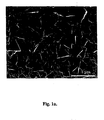
- Fig. 1a Scanning electron microscope (SEM) image of the thin film is shown in Fig. 1a.
- the film morphology reveals to consist predominantly of ⁇ 111 ⁇ facets with a mean grain size of 1 ⁇ m.
- Scarce detections of (220), (311) and (400) peaks suggest the ⁇ 111 ⁇ textured growth of the film.
- the transport properties were measured between room temperature and 1.7K.
- Fig. 2a shows the temperature dependence of resistivity of the thin film under several values of magnetic fields up to 9T.
- the resistivity With decreasing temperature, the resistivity initially decreases slightly but increases gradually below 200K.
- the resistivity began to drop at around 7K which corresponds to the onset of a superconducting transition, and dropped to zero at around 4.2K (Tc offset) in the absent of the field.
- the superconducting transition temperature is shifted with the increasing of the applied field.
- the field dependence of the onsets and offsets of Tc are plotted in Fig. 2b.
- the extrapolation of Tc onset approaches the value of 10.4 T.
- the upper critical field Hc 2 is estimated to be 7 T. This value is roughly similar to the Hc 2 of c-axis direction in MgB 2 .
- the irreversibility field is found to be 5.12 T at 0K.
- the magnetization properties were measured by a superconducting quantum interface device (SQUID) magnetometer down to 1.78K.
- the temperature dependence of the magnetization is plotted in Fig 3a.
- Diamagnetic signals corresponding to superconductivity appeared below 4K where the resistance drops to zero.
- the large difference between the zero-field cooling (ZFC) and field cooling (FC) curvatures indicates that the material has a fairly large flux pinning force resulting in the trapping of magnetic flux in the field cooling condition.
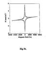
- Magnetization versus magnetic field (M-H) curvature obtained at 1.8K was plotted in Fig. 3b.
- Large symmetric hysteresis curvature shows the characteristics of typical type II superconductor.
- AM emu/cm 3
- J C 30 x ⁇ M /d, where d is the size of the sample.
- the J C at 0T is estimated to be 200 A/cm 2 .
- the hardest superconducting wires will be fabricated.
Landscapes
- Chemical & Material Sciences (AREA)
- Engineering & Computer Science (AREA)
- Mechanical Engineering (AREA)
- Chemical Kinetics & Catalysis (AREA)
- General Chemical & Material Sciences (AREA)
- Materials Engineering (AREA)
- Inorganic Chemistry (AREA)
- Metallurgy (AREA)
- Organic Chemistry (AREA)
- Manufacturing & Machinery (AREA)
- Crystals, And After-Treatments Of Crystals (AREA)
- Carbon And Carbon Compounds (AREA)
- Chemical Vapour Deposition (AREA)
- Superconductors And Manufacturing Methods Therefor (AREA)
Abstract
Description
Claims (10)
- A boron-doped diamond thin film having superconductivity.
- A boron-doped diamond thin film as claimed in claim 1, wherein said thin film is deposited by chemical vapour deposition.
- A boron-doped diamond thin film as claimed in claim 2, wherein said chemical vapour deposition is carried out using a gas mixture of at least carbon compound, boron compound and hydrogen.
- A boron-doped diamond thin film as claimed in claim 2 or claim 3, wherein said chemical vapour deposition is microwave plasma deposition.
- A boron-doped diamond thin film as claimed in any preceding claim, wherein said thin film is (111) orientated.
- A method for the preparation of a boron-doped diamond thin film as claimed in any preceding claim comprising depositing said film on a substrate by chemical vapour deposition.
- A method as claimed in claim 6, wherein said chemical vapour deposition is carried out using a gas mixture of at least carbon compound, boron compound and hydrogen.
- A method as claimed in claim 7, wherein said boron compound is diborane, trimethylborane, boron oxide, boric acid or boron.
- A method as claimed in any one of claims 6 to 8, wherein said chemical vapour deposition is microwave plasma deposition.
- Use of a boron-doped diamond thin film as claimed in any one of claims 1 to 5 for the manufacture of an electric or electronics device.
Applications Claiming Priority (2)
| Application Number | Priority Date | Filing Date | Title |
|---|---|---|---|
| US57294804P | 2004-05-21 | 2004-05-21 | |
| US572948 | 2004-05-21 |
Publications (3)
| Publication Number | Publication Date |
|---|---|
| EP1598443A2 true EP1598443A2 (en) | 2005-11-23 |
| EP1598443A3 EP1598443A3 (en) | 2006-02-01 |
| EP1598443B1 EP1598443B1 (en) | 2008-10-08 |
Family
ID=34941419
Family Applications (1)
| Application Number | Title | Priority Date | Filing Date |
|---|---|---|---|
| EP05253160A Expired - Lifetime EP1598443B1 (en) | 2004-05-21 | 2005-05-23 | Superconductivity in boron-doped diamond thin film |
Country Status (4)
| Country | Link |
|---|---|
| US (1) | US7976893B2 (en) |
| EP (1) | EP1598443B1 (en) |
| JP (1) | JP4759315B2 (en) |
| DE (1) | DE602005010144D1 (en) |
Cited By (5)
| Publication number | Priority date | Publication date | Assignee | Title |
|---|---|---|---|---|
| CN103249864A (en) * | 2010-11-16 | 2013-08-14 | 斯沃奇集团研究及开发有限公司 | Method for coating micromechanical parts with dual diamond coating |
| CN106115685A (en) * | 2016-06-24 | 2016-11-16 | 大连理工大学 | A kind of method of Nano diamond surface boronation |
| CN112899644A (en) * | 2021-01-21 | 2021-06-04 | 山东欣远新材料科技有限公司 | Diamond film boron oxide doping method |
| WO2021228039A1 (en) * | 2020-05-11 | 2021-11-18 | 南京岱蒙特科技有限公司 | Boron-doped diamond electrode with ultra-high specific surface area, and preparation method therefor and use thereof |
| WO2021228038A1 (en) * | 2020-05-11 | 2021-11-18 | 南京岱蒙特科技有限公司 | High-specific surface area and super-hydrophilic gradient boron-doped diamond electrode, preparation method therefor and application thereof |
Families Citing this family (8)
| Publication number | Priority date | Publication date | Assignee | Title |
|---|---|---|---|---|
| JP5496585B2 (en) * | 2009-09-04 | 2014-05-21 | 独立行政法人物質・材料研究機構 | Josephson element |
| KR101034761B1 (en) * | 2009-11-20 | 2011-05-18 | 우석대학교 산학협력단 | Estimation Method of Critical Current Density of Superconducting Wire Using Measurement of Magnetization Loss |
| BE1019439A3 (en) * | 2010-07-30 | 2012-07-03 | Diarotech | PROCESS FOR SYNTHESIZING VAPOR PHASE CHEMICAL DEPOSITION WITH SOLID MATERIAL, IN PARTICULAR DIAMOND, AND DEVICE FOR APPLYING THE PROCESS |
| CN102127751B (en) * | 2011-01-11 | 2012-12-26 | 大连理工大学 | Boron-doped diamond micro-nano material with columnar array structure and preparation method thereof |
| JP6241943B2 (en) * | 2014-03-14 | 2017-12-06 | 学校法人東京理科大学 | Method for producing boron-doped diamond nanoparticles |
| JP6489594B2 (en) * | 2015-08-28 | 2019-03-27 | 国立研究開発法人物質・材料研究機構 | Diamond anvil cell |
| CN107389217A (en) * | 2017-06-20 | 2017-11-24 | 西安交通大学 | A kind of temperature sensor chip based on ultra-high resistance temperature coefficient amorphous carbon film |
| JP7539146B2 (en) * | 2020-12-03 | 2024-08-23 | 国立研究開発法人物質・材料研究機構 | Diamond anvil cell and high pressure physical property measurement device |
Family Cites Families (12)
| Publication number | Priority date | Publication date | Assignee | Title |
|---|---|---|---|---|
| JP2730144B2 (en) * | 1989-03-07 | 1998-03-25 | 住友電気工業株式会社 | Single crystal diamond layer formation method |
| GB9111474D0 (en) | 1991-05-29 | 1991-07-17 | De Beers Ind Diamond | Boron doped diamond |
| JPH061695A (en) * | 1992-06-25 | 1994-01-11 | Idemitsu Petrochem Co Ltd | Method for synthesizing diamond |
| US5698328A (en) * | 1994-04-06 | 1997-12-16 | The Regents Of The University Of California | Diamond thin film electron emitter |
| CA2185217A1 (en) | 1994-04-06 | 1995-10-19 | The Regents Of The University Of California | Process to produce diamond films |
| JP3041844B2 (en) * | 1995-08-11 | 2000-05-15 | 住友電気工業株式会社 | Film forming or etching equipment |
| KR100253115B1 (en) * | 1997-03-05 | 2000-05-01 | 윤덕용 | Fabrication method of n type semiconductor |
| US6858080B2 (en) * | 1998-05-15 | 2005-02-22 | Apollo Diamond, Inc. | Tunable CVD diamond structures |
| US6274837B1 (en) * | 1999-06-16 | 2001-08-14 | Saint-Gobain Industrial Ceramics, Inc. | Method and apparatus for in-situ solid state doping of CVD diamonds and diamonds so made |
| JP3971090B2 (en) * | 2000-04-05 | 2007-09-05 | 株式会社神戸製鋼所 | Method for producing diamond having needle-like surface and method for producing carbon-based material having cilia-like surface |
| JP2003321296A (en) | 2002-04-25 | 2003-11-11 | Shin Etsu Chem Co Ltd | Diamond film and method of manufacturing the same |
| US7312562B2 (en) * | 2004-02-04 | 2007-12-25 | Chevron U.S.A. Inc. | Heterodiamondoid-containing field emission devices |
-
2005
- 2005-05-20 JP JP2005148794A patent/JP4759315B2/en not_active Expired - Fee Related
- 2005-05-20 US US11/133,269 patent/US7976893B2/en not_active Expired - Fee Related
- 2005-05-23 EP EP05253160A patent/EP1598443B1/en not_active Expired - Lifetime
- 2005-05-23 DE DE602005010144T patent/DE602005010144D1/en not_active Expired - Lifetime
Cited By (6)
| Publication number | Priority date | Publication date | Assignee | Title |
|---|---|---|---|---|
| CN103249864A (en) * | 2010-11-16 | 2013-08-14 | 斯沃奇集团研究及开发有限公司 | Method for coating micromechanical parts with dual diamond coating |
| CN103249864B (en) * | 2010-11-16 | 2016-05-18 | 斯沃奇集团研究及开发有限公司 | By the method for two diamond coatings coating micromechanical parts |
| CN106115685A (en) * | 2016-06-24 | 2016-11-16 | 大连理工大学 | A kind of method of Nano diamond surface boronation |
| WO2021228039A1 (en) * | 2020-05-11 | 2021-11-18 | 南京岱蒙特科技有限公司 | Boron-doped diamond electrode with ultra-high specific surface area, and preparation method therefor and use thereof |
| WO2021228038A1 (en) * | 2020-05-11 | 2021-11-18 | 南京岱蒙特科技有限公司 | High-specific surface area and super-hydrophilic gradient boron-doped diamond electrode, preparation method therefor and application thereof |
| CN112899644A (en) * | 2021-01-21 | 2021-06-04 | 山东欣远新材料科技有限公司 | Diamond film boron oxide doping method |
Also Published As
| Publication number | Publication date |
|---|---|
| JP2006009147A (en) | 2006-01-12 |
| JP4759315B2 (en) | 2011-08-31 |
| DE602005010144D1 (en) | 2008-11-20 |
| EP1598443B1 (en) | 2008-10-08 |
| EP1598443A3 (en) | 2006-02-01 |
| US20060035788A1 (en) | 2006-02-16 |
| US7976893B2 (en) | 2011-07-12 |
Similar Documents
| Publication | Publication Date | Title |
|---|---|---|
| Takano et al. | Superconductivity in diamond thin films well above liquid helium temperature | |
| Takano et al. | Superconducting properties of homoepitaxial CVD diamond | |
| Yamamoto et al. | Improved critical current properties observed in MgB2 bulks synthesized by low-temperature solid-state reaction | |
| Imai et al. | Systematic comparison of eight substrates in the growth of FeSe0. 5Te0. 5 superconducting thin films | |
| Nie et al. | Suppression of superconductivity in FeSe films under tensile strain | |
| EP1598443B1 (en) | Superconductivity in boron-doped diamond thin film | |
| Adenwalla et al. | Boron carbide/n-silicon carbide heterojunction diodes | |
| Xu et al. | Quasi-aligned ZnO nanotubes grown on Si substrates | |
| JP2013545213A (en) | Iron-based superconducting structure and manufacturing method thereof | |
| Imai et al. | Superconductivity of FeSe0. 5Te0. 5 thin films grown by pulsed laser deposition | |
| Eng et al. | Influence of pulsed laser deposition growth conditions on the thermoelectric properties of Ca3Co4O9 thin films | |
| US20060093861A1 (en) | Method for producing doped, alloyed, and mixed-phase magnesium boride films | |
| WO2003082482A1 (en) | Method for producing boride thin films | |
| Li et al. | Highly conductive and flexible electrodes based on ultrathin aluminum-doped zinc oxide epitaxial films | |
| Huang et al. | Superconducting iron chalcogenide thin films integrated on flexible mica substrates | |
| Pang et al. | Synthesis and thermoelectric properties of Bi-doped SnSe thin films | |
| Ranot et al. | MgB2 coated superconducting tapes with high critical current densities fabricated by hybrid physical–chemical vapor deposition | |
| Gao et al. | Bulk superconductivity in quasi-one-dimensional ZrS e 3 under high pressure | |
| Kang et al. | Growth of HgBa 2 Ca 2 Cu 3 O 8 thin films using stable Re 0.1 Ba 2 Ca 2 Cu 3 O x precursor by pulsed laser deposition | |
| Jia et al. | The role of a superconducting seed layer in the structural and transport properties of EuBa 2 Cu 3 O 7− x films | |
| Gu et al. | Bulk superconductivity in one-step grown Fe (Te, Se) crystals free of interstitial iron by minor Mn doping | |
| Mele et al. | Fabrication of Fe–Te–S Superconducting Epitaxial Thin Films by Pulsed Laser Deposition | |
| Liu et al. | Transparent ZnO: Al2O3 films with high breakdown voltage and resistivity | |
| Wang et al. | Growth dynamics controllable deposition of homoepitaxial MgO films on the IBAD-MgO substrates | |
| Mohan Kant et al. | Magnetic and optical properties of rare earth doped Sn0. 95RE0. 05O2− δ (RE= Gd, Dy, Er) |
Legal Events
| Date | Code | Title | Description |
|---|---|---|---|
| PUAI | Public reference made under article 153(3) epc to a published international application that has entered the european phase |
Free format text: ORIGINAL CODE: 0009012 |
|
| AK | Designated contracting states |
Kind code of ref document: A2 Designated state(s): AT BE BG CH CY CZ DE DK EE ES FI FR GB GR HU IE IS IT LI LT LU MC NL PL PT RO SE SI SK TR |
|
| AX | Request for extension of the european patent |
Extension state: AL BA HR LV MK YU |
|
| PUAL | Search report despatched |
Free format text: ORIGINAL CODE: 0009013 |
|
| AK | Designated contracting states |
Kind code of ref document: A3 Designated state(s): AT BE BG CH CY CZ DE DK EE ES FI FR GB GR HU IE IS IT LI LT LU MC NL PL PT RO SE SI SK TR |
|
| AX | Request for extension of the european patent |
Extension state: AL BA HR LV MK YU |
|
| 17P | Request for examination filed |
Effective date: 20060509 |
|
| 17Q | First examination report despatched |
Effective date: 20060828 |
|
| AKX | Designation fees paid |
Designated state(s): DE FR GB |
|
| GRAP | Despatch of communication of intention to grant a patent |
Free format text: ORIGINAL CODE: EPIDOSNIGR1 |
|
| GRAS | Grant fee paid |
Free format text: ORIGINAL CODE: EPIDOSNIGR3 |
|
| GRAA | (expected) grant |
Free format text: ORIGINAL CODE: 0009210 |
|
| AK | Designated contracting states |
Kind code of ref document: B1 Designated state(s): DE FR GB |
|
| REG | Reference to a national code |
Ref country code: GB Ref legal event code: FG4D |
|
| REF | Corresponds to: |
Ref document number: 602005010144 Country of ref document: DE Date of ref document: 20081120 Kind code of ref document: P |
|
| PLBE | No opposition filed within time limit |
Free format text: ORIGINAL CODE: 0009261 |
|
| STAA | Information on the status of an ep patent application or granted ep patent |
Free format text: STATUS: NO OPPOSITION FILED WITHIN TIME LIMIT |
|
| 26N | No opposition filed |
Effective date: 20090709 |
|
| PGFP | Annual fee paid to national office [announced via postgrant information from national office to epo] |
Ref country code: GB Payment date: 20140521 Year of fee payment: 10 |
|
| PGFP | Annual fee paid to national office [announced via postgrant information from national office to epo] |
Ref country code: FR Payment date: 20140527 Year of fee payment: 10 Ref country code: DE Payment date: 20140521 Year of fee payment: 10 |
|
| REG | Reference to a national code |
Ref country code: DE Ref legal event code: R119 Ref document number: 602005010144 Country of ref document: DE |
|
| GBPC | Gb: european patent ceased through non-payment of renewal fee |
Effective date: 20150523 |
|
| REG | Reference to a national code |
Ref country code: FR Ref legal event code: ST Effective date: 20160129 |
|
| PG25 | Lapsed in a contracting state [announced via postgrant information from national office to epo] |
Ref country code: GB Free format text: LAPSE BECAUSE OF NON-PAYMENT OF DUE FEES Effective date: 20150523 Ref country code: DE Free format text: LAPSE BECAUSE OF NON-PAYMENT OF DUE FEES Effective date: 20151201 |
|
| PG25 | Lapsed in a contracting state [announced via postgrant information from national office to epo] |
Ref country code: FR Free format text: LAPSE BECAUSE OF NON-PAYMENT OF DUE FEES Effective date: 20150601 |