EP1596460A1 - Light-detectable solid thin-film secondary battery - Google Patents
Light-detectable solid thin-film secondary battery Download PDFInfo
- Publication number
- EP1596460A1 EP1596460A1 EP03768384A EP03768384A EP1596460A1 EP 1596460 A1 EP1596460 A1 EP 1596460A1 EP 03768384 A EP03768384 A EP 03768384A EP 03768384 A EP03768384 A EP 03768384A EP 1596460 A1 EP1596460 A1 EP 1596460A1
- Authority
- EP
- European Patent Office
- Prior art keywords
- light
- secondary cell
- active material
- electrode active
- photosensitive
- Prior art date
- Legal status (The legal status is an assumption and is not a legal conclusion. Google has not performed a legal analysis and makes no representation as to the accuracy of the status listed.)
- Granted
Links
- 239000010409 thin film Substances 0.000 title claims abstract description 41
- 239000007787 solid Substances 0.000 title 1
- 229910021426 porous silicon Inorganic materials 0.000 claims abstract description 23
- 238000001514 detection method Methods 0.000 claims abstract description 22
- 239000007773 negative electrode material Substances 0.000 claims abstract description 20
- 229910001416 lithium ion Inorganic materials 0.000 claims abstract description 18
- HBBGRARXTFLTSG-UHFFFAOYSA-N Lithium ion Chemical compound [Li+] HBBGRARXTFLTSG-UHFFFAOYSA-N 0.000 claims abstract description 16
- 230000008859 change Effects 0.000 claims abstract description 7
- 239000000758 substrate Substances 0.000 claims description 18
- 239000007774 positive electrode material Substances 0.000 claims description 16
- 239000010408 film Substances 0.000 claims description 15
- XUIMIQQOPSSXEZ-UHFFFAOYSA-N Silicon Chemical compound [Si] XUIMIQQOPSSXEZ-UHFFFAOYSA-N 0.000 claims description 14
- 229910052710 silicon Inorganic materials 0.000 claims description 14
- 239000010703 silicon Substances 0.000 claims description 14
- 238000007743 anodising Methods 0.000 claims description 8
- 239000007784 solid electrolyte Substances 0.000 claims description 8
- 230000035945 sensitivity Effects 0.000 claims description 6
- 239000000203 mixture Substances 0.000 claims description 3
- 239000002131 composite material Substances 0.000 claims description 2
- 238000002834 transmittance Methods 0.000 claims description 2
- 238000012423 maintenance Methods 0.000 abstract description 2
- 239000013078 crystal Substances 0.000 description 8
- 230000007423 decrease Effects 0.000 description 7
- 230000004044 response Effects 0.000 description 7
- 206010034960 Photophobia Diseases 0.000 description 6
- 208000013469 light sensitivity Diseases 0.000 description 6
- 238000007599 discharging Methods 0.000 description 5
- 229910002097 Lithium manganese(III,IV) oxide Inorganic materials 0.000 description 4
- 238000002048 anodisation reaction Methods 0.000 description 4
- 230000003247 decreasing effect Effects 0.000 description 4
- 238000001228 spectrum Methods 0.000 description 4
- 230000007704 transition Effects 0.000 description 4
- 230000005611 electricity Effects 0.000 description 3
- LFQSCWFLJHTTHZ-UHFFFAOYSA-N Ethanol Chemical compound CCO LFQSCWFLJHTTHZ-UHFFFAOYSA-N 0.000 description 2
- KRHYYFGTRYWZRS-UHFFFAOYSA-N Fluorane Chemical compound F KRHYYFGTRYWZRS-UHFFFAOYSA-N 0.000 description 2
- 229910012776 Li3PO4-xNx Inorganic materials 0.000 description 2
- 238000010586 diagram Methods 0.000 description 2
- 239000000463 material Substances 0.000 description 2
- 238000005259 measurement Methods 0.000 description 2
- 230000003287 optical effect Effects 0.000 description 2
- 230000002093 peripheral effect Effects 0.000 description 2
- 229910021420 polycrystalline silicon Inorganic materials 0.000 description 2
- 238000001552 radio frequency sputter deposition Methods 0.000 description 2
- 229910012813 Li3PO4−xNx Inorganic materials 0.000 description 1
- 230000005856 abnormality Effects 0.000 description 1
- 239000011149 active material Substances 0.000 description 1
- 230000005540 biological transmission Effects 0.000 description 1
- 230000015572 biosynthetic process Effects 0.000 description 1
- 229910021419 crystalline silicon Inorganic materials 0.000 description 1
- 230000003111 delayed effect Effects 0.000 description 1
- 238000005265 energy consumption Methods 0.000 description 1
- 238000005516 engineering process Methods 0.000 description 1
- 239000011521 glass Substances 0.000 description 1
- 150000002500 ions Chemical class 0.000 description 1
- 238000010030 laminating Methods 0.000 description 1
- 238000004519 manufacturing process Methods 0.000 description 1
- 229910052751 metal Inorganic materials 0.000 description 1
- 239000002184 metal Substances 0.000 description 1
- 238000000034 method Methods 0.000 description 1
- 239000013081 microcrystal Substances 0.000 description 1
- 230000005012 migration Effects 0.000 description 1
- 238000013508 migration Methods 0.000 description 1
- 238000012544 monitoring process Methods 0.000 description 1
- 230000000149 penetrating effect Effects 0.000 description 1
- 230000008569 process Effects 0.000 description 1
- 238000011084 recovery Methods 0.000 description 1
- 230000009467 reduction Effects 0.000 description 1
- 239000004065 semiconductor Substances 0.000 description 1
- 230000008054 signal transmission Effects 0.000 description 1
- 239000002409 silicon-based active material Substances 0.000 description 1
- 230000005476 size effect Effects 0.000 description 1
- 230000003595 spectral effect Effects 0.000 description 1
- 238000004544 sputter deposition Methods 0.000 description 1
- 239000000126 substance Substances 0.000 description 1
- 229910052720 vanadium Inorganic materials 0.000 description 1
- LEONUFNNVUYDNQ-UHFFFAOYSA-N vanadium atom Chemical compound [V] LEONUFNNVUYDNQ-UHFFFAOYSA-N 0.000 description 1
Images


Classifications
-
- H—ELECTRICITY
- H01—ELECTRIC ELEMENTS
- H01M—PROCESSES OR MEANS, e.g. BATTERIES, FOR THE DIRECT CONVERSION OF CHEMICAL ENERGY INTO ELECTRICAL ENERGY
- H01M6/00—Primary cells; Manufacture thereof
- H01M6/40—Printed batteries, e.g. thin film batteries
-
- G—PHYSICS
- G01—MEASURING; TESTING
- G01J—MEASUREMENT OF INTENSITY, VELOCITY, SPECTRAL CONTENT, POLARISATION, PHASE OR PULSE CHARACTERISTICS OF INFRARED, VISIBLE OR ULTRAVIOLET LIGHT; COLORIMETRY; RADIATION PYROMETRY
- G01J1/00—Photometry, e.g. photographic exposure meter
- G01J1/42—Photometry, e.g. photographic exposure meter using electric radiation detectors
-
- H—ELECTRICITY
- H01—ELECTRIC ELEMENTS
- H01G—CAPACITORS; CAPACITORS, RECTIFIERS, DETECTORS, SWITCHING DEVICES, LIGHT-SENSITIVE OR TEMPERATURE-SENSITIVE DEVICES OF THE ELECTROLYTIC TYPE
- H01G9/00—Electrolytic capacitors, rectifiers, detectors, switching devices, light-sensitive or temperature-sensitive devices; Processes of their manufacture
- H01G9/20—Light-sensitive devices
- H01G9/2004—Light-sensitive devices characterised by the electrolyte, e.g. comprising an organic electrolyte
- H01G9/2009—Solid electrolytes
-
- H—ELECTRICITY
- H01—ELECTRIC ELEMENTS
- H01M—PROCESSES OR MEANS, e.g. BATTERIES, FOR THE DIRECT CONVERSION OF CHEMICAL ENERGY INTO ELECTRICAL ENERGY
- H01M10/00—Secondary cells; Manufacture thereof
- H01M10/04—Construction or manufacture in general
- H01M10/0436—Small-sized flat cells or batteries for portable equipment
-
- H—ELECTRICITY
- H01—ELECTRIC ELEMENTS
- H01M—PROCESSES OR MEANS, e.g. BATTERIES, FOR THE DIRECT CONVERSION OF CHEMICAL ENERGY INTO ELECTRICAL ENERGY
- H01M10/00—Secondary cells; Manufacture thereof
- H01M10/05—Accumulators with non-aqueous electrolyte
- H01M10/052—Li-accumulators
- H01M10/0525—Rocking-chair batteries, i.e. batteries with lithium insertion or intercalation in both electrodes; Lithium-ion batteries
-
- H—ELECTRICITY
- H01—ELECTRIC ELEMENTS
- H01M—PROCESSES OR MEANS, e.g. BATTERIES, FOR THE DIRECT CONVERSION OF CHEMICAL ENERGY INTO ELECTRICAL ENERGY
- H01M10/00—Secondary cells; Manufacture thereof
- H01M10/42—Methods or arrangements for servicing or maintenance of secondary cells or secondary half-cells
- H01M10/48—Accumulators combined with arrangements for measuring, testing or indicating the condition of cells, e.g. the level or density of the electrolyte
- H01M10/488—Cells or batteries combined with indicating means for external visualization of the condition, e.g. by change of colour or of light density
-
- H—ELECTRICITY
- H01—ELECTRIC ELEMENTS
- H01M—PROCESSES OR MEANS, e.g. BATTERIES, FOR THE DIRECT CONVERSION OF CHEMICAL ENERGY INTO ELECTRICAL ENERGY
- H01M14/00—Electrochemical current or voltage generators not provided for in groups H01M6/00 - H01M12/00; Manufacture thereof
- H01M14/005—Photoelectrochemical storage cells
-
- H—ELECTRICITY
- H01—ELECTRIC ELEMENTS
- H01M—PROCESSES OR MEANS, e.g. BATTERIES, FOR THE DIRECT CONVERSION OF CHEMICAL ENERGY INTO ELECTRICAL ENERGY
- H01M4/00—Electrodes
- H01M4/02—Electrodes composed of, or comprising, active material
- H01M4/13—Electrodes for accumulators with non-aqueous electrolyte, e.g. for lithium-accumulators; Processes of manufacture thereof
- H01M4/134—Electrodes based on metals, Si or alloys
-
- H—ELECTRICITY
- H01—ELECTRIC ELEMENTS
- H01M—PROCESSES OR MEANS, e.g. BATTERIES, FOR THE DIRECT CONVERSION OF CHEMICAL ENERGY INTO ELECTRICAL ENERGY
- H01M4/00—Electrodes
- H01M4/02—Electrodes composed of, or comprising, active material
- H01M4/36—Selection of substances as active materials, active masses, active liquids
- H01M4/38—Selection of substances as active materials, active masses, active liquids of elements or alloys
- H01M4/386—Silicon or alloys based on silicon
-
- H—ELECTRICITY
- H01—ELECTRIC ELEMENTS
- H01M—PROCESSES OR MEANS, e.g. BATTERIES, FOR THE DIRECT CONVERSION OF CHEMICAL ENERGY INTO ELECTRICAL ENERGY
- H01M10/00—Secondary cells; Manufacture thereof
- H01M10/05—Accumulators with non-aqueous electrolyte
- H01M10/052—Li-accumulators
-
- H—ELECTRICITY
- H01—ELECTRIC ELEMENTS
- H01M—PROCESSES OR MEANS, e.g. BATTERIES, FOR THE DIRECT CONVERSION OF CHEMICAL ENERGY INTO ELECTRICAL ENERGY
- H01M10/00—Secondary cells; Manufacture thereof
- H01M10/05—Accumulators with non-aqueous electrolyte
- H01M10/056—Accumulators with non-aqueous electrolyte characterised by the materials used as electrolytes, e.g. mixed inorganic/organic electrolytes
- H01M10/0561—Accumulators with non-aqueous electrolyte characterised by the materials used as electrolytes, e.g. mixed inorganic/organic electrolytes the electrolyte being constituted of inorganic materials only
- H01M10/0562—Solid materials
-
- H—ELECTRICITY
- H01—ELECTRIC ELEMENTS
- H01M—PROCESSES OR MEANS, e.g. BATTERIES, FOR THE DIRECT CONVERSION OF CHEMICAL ENERGY INTO ELECTRICAL ENERGY
- H01M4/00—Electrodes
- H01M4/02—Electrodes composed of, or comprising, active material
- H01M2004/021—Physical characteristics, e.g. porosity, surface area
-
- Y—GENERAL TAGGING OF NEW TECHNOLOGICAL DEVELOPMENTS; GENERAL TAGGING OF CROSS-SECTIONAL TECHNOLOGIES SPANNING OVER SEVERAL SECTIONS OF THE IPC; TECHNICAL SUBJECTS COVERED BY FORMER USPC CROSS-REFERENCE ART COLLECTIONS [XRACs] AND DIGESTS
- Y02—TECHNOLOGIES OR APPLICATIONS FOR MITIGATION OR ADAPTATION AGAINST CLIMATE CHANGE
- Y02E—REDUCTION OF GREENHOUSE GAS [GHG] EMISSIONS, RELATED TO ENERGY GENERATION, TRANSMISSION OR DISTRIBUTION
- Y02E10/00—Energy generation through renewable energy sources
- Y02E10/50—Photovoltaic [PV] energy
- Y02E10/542—Dye sensitized solar cells
-
- Y—GENERAL TAGGING OF NEW TECHNOLOGICAL DEVELOPMENTS; GENERAL TAGGING OF CROSS-SECTIONAL TECHNOLOGIES SPANNING OVER SEVERAL SECTIONS OF THE IPC; TECHNICAL SUBJECTS COVERED BY FORMER USPC CROSS-REFERENCE ART COLLECTIONS [XRACs] AND DIGESTS
- Y02—TECHNOLOGIES OR APPLICATIONS FOR MITIGATION OR ADAPTATION AGAINST CLIMATE CHANGE
- Y02E—REDUCTION OF GREENHOUSE GAS [GHG] EMISSIONS, RELATED TO ENERGY GENERATION, TRANSMISSION OR DISTRIBUTION
- Y02E60/00—Enabling technologies; Technologies with a potential or indirect contribution to GHG emissions mitigation
- Y02E60/10—Energy storage using batteries
-
- Y—GENERAL TAGGING OF NEW TECHNOLOGICAL DEVELOPMENTS; GENERAL TAGGING OF CROSS-SECTIONAL TECHNOLOGIES SPANNING OVER SEVERAL SECTIONS OF THE IPC; TECHNICAL SUBJECTS COVERED BY FORMER USPC CROSS-REFERENCE ART COLLECTIONS [XRACs] AND DIGESTS
- Y02—TECHNOLOGIES OR APPLICATIONS FOR MITIGATION OR ADAPTATION AGAINST CLIMATE CHANGE
- Y02P—CLIMATE CHANGE MITIGATION TECHNOLOGIES IN THE PRODUCTION OR PROCESSING OF GOODS
- Y02P70/00—Climate change mitigation technologies in the production process for final industrial or consumer products
- Y02P70/50—Manufacturing or production processes characterised by the final manufactured product
Definitions
- the present invention relates to all-solid-state thin-film secondary cells having a photosensitive function and photodetectors loaded with the secondary cells.
- Porous silicon is known as a light-emitting element or a light-emitting and receiving element (for example, see Patent Document 1).
- a photodetector using direct-transition-type porous silicon is also known (for example, see Patent Document 2).
- Patent Document 1 Japanese Unexamined Patent Application Publication No. 4-356977 (Japanese Patent No. 3306077)
- Patent Document 2 Japanese Unexamined Patent Application Publication No. 5-37000 (Japanese Patent No.
- the inventors have developed a solid-state thin-film secondary cell having a novel configuration combining a photosensitive function with a negative-electrode active material layer for the solid-state thin-film secondary cell.
- the present invention is as follows:
- Conventional photoconductive cells and photodiodes detect current flows caused by incident light or voltages caused by the current flows in both sides of external resistors, namely, they are a current type or an energy-consumption type.
- the photosensitive solid-state thin-film secondary cell of the present invention detects a change in voltage between positive-electrode and negative-electrode terminals of the cell caused by electrons and positive holes induced to the negative electrode (porous silicon). Basically, incident light does not cause current at all. This is because ion current produced by shuttling lithium ions between the positive-electrode and the negative-electrode terminals flows in the cell, and electronic current penetrating between the positive-electrode and the negative electrode cannot flow in the cell.
- the photosensitive solid-state thin-film secondary cell of the present invention is a voltage type or an energy-nonconsumption type. No discharge caused by continuous irradiation of light occurs in the cell. Only self-discharge slowly proceeds. This is the same as in unused cells during storage.
- the photosensitive solid-state thin-film secondary cell of the present invention is suitable for driving electronic devices in a controlling manner.
- the number of items or heads is counted by detecting an increase in voltage in both terminals of the cell, the increase is generated by interruption of natural light (sunlight) during the daytime or interior light during the night by something; and security during the night is managed by detecting an increase in voltage generated by interruption of artificial light in an invisible near-infrared range from a light-emitting diode or a laser diode.
- Power supply to electronic devices is generally performed by sending signals through electronic circuits (wired, therefore, contact circuits).
- electronic circuits wireless, therefore, contact circuits.
- radio transmission light rays, therefore, noncontact manner
- a component for receiving the light signals is necessary.
- the photosensitive solid-state thin-film secondary cell can constitute a component having its own cell for driving the component itself.
- a power supply (cell) unit which can control discharging electricity in a cell by temporarily decreasing the terminal voltage of the cell to lower than a threshold level with external light signals to stop the electrical supply to a load from the cell temporarily or for a predetermined period of time, or a photosensitive controller which has an own electricity-supplying function can be achieved.
- Light-detecting modes are categorized to a direct-current mode (steady light mode) and an alternate-current mode (on-off mode).
- the direct-current mode the surface of the secondary cell is constantly irradiated with visible light or near-infrared light (invisible light).
- visible light near-infrared light
- the interruption is detected as an increase in voltage generated in the terminals of the cell. For example, this can be applied to a component of a security system.
- a change in luminance from night to daytime can be detected as a decrease in voltage generated in the terminals of the cell, thus, daybreak is recognized and electrical devices are switched on (or off).
- this can be applied for driving unmanned electronic devices in the daytime or the night only.
- the number of items or heads interrupting light is counted (increasing-voltage type) with a time resolution in the order of milliseconds, or light-flashing frequency is counted (decreasing-voltage type).
- Light detection using the photosensitive solid-state thin-film secondary cell of the present invention is performed via an open-circuit condition of the secondary cell or a sufficiently large resistance. Therefore, the light detection can be performed under a condition substantially the same as that of a secondary cell in storage or unused (self-discharging condition) and cell capacity is rarely drained (basically, drain by self-discharge only).
- FIGs. 1 and 2 are schematic views of photosensitive solid-state thin-film secondary cells according to embodiments of the present invention.
- a basic configuration of the cells includes a substrate 1, a negative-electrode active material layer 2, a solid electrolyte layer 3, a positive-electrode active material layer 4, and a current collector layer 5 in this order.
- a positive-electrode terminal 6 is disposed on the current collector layer 5, and a negative-electrode terminal 7 is disposed on the negative-electrode active material layer 2.
- the terminals 6 and 7 are connected to a circuit or a device for monitoring (detecting) voltage abnormality (voltage rise or fall) between the terminals of the cell.
- the structures of the solid electrolyte layer 3, the positive-electrode active material layer 4, and the current collector layer 5 are the same as those of common solid-state thin-film lithium-ion secondary cell, but the negative-electrode active material layer 2 is made of a material having light sensitivity.
- Porous silicon can be used as such an active material.
- Porous silicon has peculiar silicon crystals including a skeleton structure produced by a anodizing process and a remaining crystalline portion having a thickness (skeleton thickness) of about several nanometers to ten and several nanometers.
- Silicon crystals have a band-gap energy of 1.1 eV because of their energy-band structure, so they are sensitive to only light having a wavelength longer than about 1.1 ⁇ m. In such a case, since the optical transition is indirect, the optical transition efficiency is disadvantageously low. However, a reduction in size of the silicon microcrystals to the above-mentioned size enhances a band-gap energy by a quantum size effect and also changes the indirect transition into direct transition. As a result, the silicon crystals are dramatically changed to be effectively sensitive to visible light having a short wavelength. These properties of porous silicon are known.
- a substrate is formed by laminating polycrystalline silicon on a glass substrate coated with a transparent conductive film, and then the surface of the polycrystalline silicon is treated for anodization.
- a substrate of a silicon monocrystal may be treated for anodization.
- sensitivity to ultraviolet light and visible light having a short wavelength is observed. Namely, light detection over a broad wavelength range including a near-infrared light range, the entire visible light range, and an ultraviolet light range is possible by controlling the porosity by conditions for the anodization.
- a structural microporous layer effectively functions as a receiving layer for receiving lithium ions, and an efficient performance of a secondary cell is achieved by the ease in receiving and emitting of lithium ions. Furthermore, light detection in a broad wavelength range from near-infrared light to visible light can be achieved.
- the secondary cell in the secondary cell according to the present invention, all of the current collector (which includes a transparent conductive film), the positive-electrode material, and the solid electrolyte (a transparent film is used in this embodiment) are transparent.
- semitransparent ⁇ materials are not useless for the detection; for example, in a thin film having a transmissivity of 50%, a light detection sensitivity is merely decreased to a half.
- the positive-electrode active material layer considerably absorbs visible light, as shown in Fig. 2, incidence efficiency of light from the positive-electrode side can be increased by forming the positive-electrode active material layer 4 disposed as an upper layer in a stripe pattern (linear pattern) or in a mesh pattern (grid pattern); thus, the light detection sensitivity can be improved.
- a film, such as a Li 3 PO 4-X N X film, used as the solid electrolyte layer 3 is usually transparent over the entire visible light range.
- extraneous light L shown by arrows in Figs. 1 and 2 enters in the negative-electrode active material layer 2 with a photosensitive function, resulting in a change in the open-circuit voltage of the cell; thus, extraneous light can be constantly detected.
- a monolithic photodetector loaded with the secondary cell which is mountable on a single semiconductor substrate as in an LSI by integrating necessary peripheral electronic circuits on the single silicon substrate with the solid-state thin-film secondary cell, can be readily achieved.
- a negative-electrode active material layer made of porous silicon was formed by anodizing a silicon substrate under the following conditions.
- a Si substrate: (100) crystal face and a resistivity of 4 to 7 ⁇ cm, a chemical solution: a mixture of 40 wt% hydrofluoric acid: 99.5 wt% ethanol 1:1, an anodizing current density: 5 mA/cm 2 , anodizing time: 1 min, anodizing temperature and environment: 0°C in the dark, and a film thickness of porous silicon: 0.23 ⁇ m.
- a solid electrolyte layer, a positive-electrode active material layer, and a current collector layer were formed under the following conditions.
- a light detection property of the resulting secondary cell was examined.
- Terminal voltage in measuring charge and discharge was measured by a source meter (KEITHLEY 2400), spectral response was measured by a digital multimeter (KEITHLEY DMM 196), and time response of light was measured by an oscilloscope (KIKUSUI 7202A).
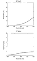
- Fig. 3 is a graph showing a transmissivity characteristic of a positive-electrode active material LiMn 2 O 4 film used in this embodiment.
- Fig. 4 is a graph showing a transmissivity characteristic of a current collector V film used in this embodiment.
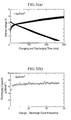
- Fig. 5(a) is a graph showing charge and discharge characteristics of this solid-state thin-film lithium-ion secondary cell in the dark.
- the charge and discharge curves are the results when the charge and discharge were repeated about 50 cycles.
- a high terminal voltage of about 3 volts was observed at the start of discharge and a discharging capacity was about 7 ⁇ Ah/cm 2 ; thus, the secondary cell showed a relatively good performance.
- Fig. 5(b) shows discharging capacity plotted against the number of repeated cycles. The capacity was increased in the beginning when the charge and discharge cycles were repeated about 50 cycles, but then the capacity was maintained substantially constant. In the range shown in the graph, no decrease was observed. This also proves that the solid-state thin-film secondary cell using the porous silicon layer as the negative-electrode active material was excellent in repeatability and reliability.
- Fig. 6 is a graph showing terminal voltage response characteristics by switching on and off an interior light (overhead fluorescent light) during the measurement of charging characteristics in the dark. The result directly shows that the open-circuit voltage of the secondary cell of this embodiment responded to on/off of the interior light.
- Fig. 7 is a partially enlarged view of Fig. 6. As shown in Fig. 7, decreases in the terminal voltage were observed when the secondary cell of this embodiment placed in a camera obscura was irradiated with light from the interior light (overhead fluorescent light) by repeatedly opening a window of the camera obscura for 1 second during charge and discharge cycles. The secondary cell exhibited a significantly rapid response to light. This is one of the highly important characteristics of the secondary cell according to the present invention.
- Fig. 8 is a graph showing a wavelength spectrum of light sensitivity indicated by - ⁇ V in the terminal voltage of the secondary cell according to this embodiment. The result shows that the secondary cell of the present invention had light sensitivity in the entire visible light range (400 to 800 nm).
- the light sensitivity range can be broadened to a range including near-infrared and near-ultraviolet by modifying conditions for preparing porous silicon.
- Fig. 9 is a graph showing time-response waveforms of light sensitivity indicated by - ⁇ V in the terminal voltage of the secondary cell according to this embodiment.
- the fall of voltage when light was intercepted by a light chopper (so-called alternating light) was extremely rapid. It seemed to approximately correspond with the waveforms of light.
- rise of voltage (recovery) slightly delayed.
- the results show that the secondary cell of this embodiment can respond to an alternating light signal frequency of about 1 kHz.
- Fig. 10 is a graph showing decreasing spectra of terminal voltage depending on light intensity in the secondary cell of this embodiment.
- the light intensity (%) was adjusted by a distance of slits of a filter.
- Fig. 11 is a graph showing decreases of terminal voltage depending on light intensity in the secondary cell of this embodiment.
- the light intensity (%) was adjusted by a distance of slits of a filter.
- a pn junction is structurally indispensable. Since the function of such a photodetector is light detection only, a power supply (or battery) is necessary to drive the photodetector. Compared to this, a photosensitive solid-state thin-film secondary cell according to the present invention uses a single p-type (or n-type) Si negative-electrode active material alone. Since the negative-electrode active material also has a function for detecting light, the light detection system with a simple configuration, a low manufacturing cost, and a reduced size and weight can be provided.
- extraneous light-controlled power supplies and photosensitive components or devices including a novel configuration, for example, a controller with a photosensitive function for controlling discharged electricity in a cell caused by extraneous light and a photosensitive component or controlling device able to supply electricity by utilizing a change in terminal voltage, can be achieved.
Landscapes
- Chemical & Material Sciences (AREA)
- Chemical Kinetics & Catalysis (AREA)
- Electrochemistry (AREA)
- Engineering & Computer Science (AREA)
- General Chemical & Material Sciences (AREA)
- Manufacturing & Machinery (AREA)
- Materials Engineering (AREA)
- Power Engineering (AREA)
- Microelectronics & Electronic Packaging (AREA)
- Physics & Mathematics (AREA)
- General Physics & Mathematics (AREA)
- Spectroscopy & Molecular Physics (AREA)
- Secondary Cells (AREA)
- Light Receiving Elements (AREA)
- Battery Electrode And Active Subsutance (AREA)
Abstract
Description
- The present invention relates to all-solid-state thin-film secondary cells having a photosensitive function and photodetectors loaded with the secondary cells.
- In general, in order to detect light, for example detection of natural light or artificial light, detection of interruption of continuous incident light, and detection of frequency of pulsed light, light detection components and power supplies in addition to peripheral electronic circuits must be provided to light detection systems. In such cases, the light detection components and the power supplies are usually prepared as separated units. Porous silicon is known as a light-emitting element or a light-emitting and receiving element (for example, see Patent Document 1). A photodetector using direct-transition-type porous silicon is also known (for example, see Patent Document 2).
- Patent Document 1: Japanese Unexamined Patent Application Publication No. 4-356977 (Japanese Patent No. 3306077)
- Patent Document 2: Japanese Unexamined Patent Application Publication No. 5-37000 (Japanese Patent No.
- It is an object of the present invention to provide novel devices for constituting light detection systems with a simple configuration, a low maintenance cost, a reduced size and weight, and high reliability by integrating light detection components and power supplies.
- In order to solve the above-mentioned problems, the inventors have developed a solid-state thin-film secondary cell having a novel configuration combining a photosensitive function with a negative-electrode active material layer for the solid-state thin-film secondary cell.
- Namely, the present invention is as follows:
- (1) A photosensitive solid-state thin-film lithium-ion secondary cell including a photosensitive negative-electrode active material layer as a component, wherein extraneous light can be constantly detected by utilizing a change in open-circuit voltage of the cell caused when the extraneous light is incident on the photosensitive negative-electrode active material layer.
- (2) The photosensitive solid-state thin-film secondary cell according to aspect (1), wherein lithium ions are readily received and emitted and light in a broad wavelength range over a near-infrared light range, the entire visible light range, and a near-ultraviolet light range is detected by utilizing a porous silicon layer having a controlled porosity as the negative-electrode active material layer.
- (3) The photosensitive solid-state thin-film secondary cell according to aspect (1) or (2), wherein a composite composed of a solid electrolyte layer, a positive-electrode active material layer, and a current collector layer is disposed on the porous silicon layer on a surface of a substrate.
- (4) The photosensitive solid-state thin-film secondary cell according to any one of aspects (1) to (3), wherein each of the positive-electrode active material layer and the current collector layer has a film composition and thickness such that the overall transmittance of visible light in the range of 400 nm to 800 nm exceeds 1% on average.
- (5) The photosensitive solid-state thin-film secondary cell according to aspect (3), wherein the porous silicon layer at the surface of the substrate is formed by anodizing a surface of a silicon wafer substrate.
- (6) The photosensitive solid-state thin-film secondary cell according to any one of aspects (1) to (5), wherein a light detection sensitivity is improved by increasing incidence efficiency of light from the positive-electrode side by forming the positive-electrode active material layer disposed as an upper layer in a stripe pattern or in a mesh pattern.
- (7) A monolithic photodetector loaded with the secondary cell prepared by integrating electronic circuits and the solid-state thin-film secondary cell according to any one of aspects (1) to (6) on a single silicon substrate.
-
- Conventional photoconductive cells and photodiodes detect current flows caused by incident light or voltages caused by the current flows in both sides of external resistors, namely, they are a current type or an energy-consumption type.
- On the other hand, the photosensitive solid-state thin-film secondary cell of the present invention detects a change in voltage between positive-electrode and negative-electrode terminals of the cell caused by electrons and positive holes induced to the negative electrode (porous silicon). Basically, incident light does not cause current at all. This is because ion current produced by shuttling lithium ions between the positive-electrode and the negative-electrode terminals flows in the cell, and electronic current penetrating between the positive-electrode and the negative electrode cannot flow in the cell. From this point of view, the photosensitive solid-state thin-film secondary cell of the present invention is a voltage type or an energy-nonconsumption type. No discharge caused by continuous irradiation of light occurs in the cell. Only self-discharge slowly proceeds. This is the same as in unused cells during storage.
- If a decrease in the terminal voltage (an increase in electric potential of the negative electrode) by light-irradiation is caused by the same reason as that in usual discharge, it means that a part of Li+ ions in porous silicon active material of the negative electrode return to a LiMn2O4 side of the positive-electrode active material. However, experimental results are that the potential returns to the original level by stopping the light-irradiation. This shows that a decrease in the terminal voltage (an increase in electric potential of the negative-electrode) by light-irradiation is not caused by migration of Li+ ions. It is assumed that the electrons and positive holes generated in pairs by light-irradiation contribute to a temporary increase in the negative-electrode potential. The pairs of electron and positive-hole cannot be generated by irradiation of visible light in normal silicon crystals, it can be generated only in porous silicon.
- The photosensitive solid-state thin-film secondary cell of the present invention is suitable for driving electronic devices in a controlling manner. For example, the number of items or heads is counted by detecting an increase in voltage in both terminals of the cell, the increase is generated by interruption of natural light (sunlight) during the daytime or interior light during the night by something; and security during the night is managed by detecting an increase in voltage generated by interruption of artificial light in an invisible near-infrared range from a light-emitting diode or a laser diode.
- Power supply to electronic devices is generally performed by sending signals through electronic circuits (wired, therefore, contact circuits). In such a system, when radio transmission (light rays, therefore, noncontact manner) is required for some reason (for example, a need for electrical noise-free signal transmission), a component for receiving the light signals is necessary. The photosensitive solid-state thin-film secondary cell can constitute a component having its own cell for driving the component itself.
- Furthermore, a power supply (cell) unit which can control discharging electricity in a cell by temporarily decreasing the terminal voltage of the cell to lower than a threshold level with external light signals to stop the electrical supply to a load from the cell temporarily or for a predetermined period of time, or a photosensitive controller which has an own electricity-supplying function can be achieved.
- Discharge caused by light irradiation does not occur in the photosensitive solid-state thin-film secondary cell of the present invention. Light-detecting modes are categorized to a direct-current mode (steady light mode) and an alternate-current mode (on-off mode). In the direct-current mode, the surface of the secondary cell is constantly irradiated with visible light or near-infrared light (invisible light). When the light path is interrupted by something, the interruption is detected as an increase in voltage generated in the terminals of the cell. For example, this can be applied to a component of a security system. A change in luminance from night to daytime can be detected as a decrease in voltage generated in the terminals of the cell, thus, daybreak is recognized and electrical devices are switched on (or off). For example, this can be applied for driving unmanned electronic devices in the daytime or the night only. In the alternate-current mode, the number of items or heads interrupting light is counted (increasing-voltage type) with a time resolution in the order of milliseconds, or light-flashing frequency is counted (decreasing-voltage type).
- Light detection using the photosensitive solid-state thin-film secondary cell of the present invention is performed via an open-circuit condition of the secondary cell or a sufficiently large resistance. Therefore, the light detection can be performed under a condition substantially the same as that of a secondary cell in storage or unused (self-discharging condition) and cell capacity is rarely drained (basically, drain by self-discharge only).
-
- Fig. 1 is a schematic diagram illustrating a photosensitive solid-state thin-film secondary cell according to an embodiment of the present invention.
- Fig. 2 is a schematic diagram illustrating a photosensitive solid-state thin-film secondary cell according to another embodiment of the present invention.
- Fig. 3 is a graph showing a transmissivity characteristic of a LiMn2O4 positive-electrode active material film.
- Fig. 4 is a graph showing a transmissivity characteristic of a current collector V film.
- Fig. 5(a) is a graph showing charge and discharge characteristics of a solid-state thin-film lithium-ion secondary cell according to a first embodiment in the dark, and Fig. 5(b) is a graph showing discharging capacity of the solid-state thin-film lithium-ion secondary cell according to the first embodiment in repeated charge and discharge cycles.
- Fig. 6 is a graph showing terminal voltage response characteristics by switching on and off an interior light during the measurement of charging characteristics of the solid-state thin-film lithium-ion secondary cell according to the first embodiment in the dark.
- Fig. 7 is a partially enlarged view of Fig. 6.
- Fig. 8 is a graph showing a wavelength spectrum in light sensitivity of the solid-state thin-film lithium-ion secondary cell according to the first embodiment.
- Fig. 9 is a graph showing time-response waveforms of the terminal voltage of the solid-state thin-film lithium-ion secondary cell according to the first embodiment.
- Fig. 10 is a graph showing decreasing spectra of terminal voltage depending on light intensity in the solid-state thin-film secondary cell.
- Fig. 11 is a graph showing decreases of terminal voltage depending on light intensity in the solid-state thin-film secondary cell.
-
- Figs. 1 and 2 are schematic views of photosensitive solid-state thin-film secondary cells according to embodiments of the present invention. A basic configuration of the cells includes a
substrate 1, a negative-electrodeactive material layer 2, asolid electrolyte layer 3, a positive-electrodeactive material layer 4, and acurrent collector layer 5 in this order. A positive-electrode terminal 6 is disposed on thecurrent collector layer 5, and a negative-electrode terminal 7 is disposed on the negative-electrodeactive material layer 2. Theterminals - The structures of the
solid electrolyte layer 3, the positive-electrodeactive material layer 4, and thecurrent collector layer 5 are the same as those of common solid-state thin-film lithium-ion secondary cell, but the negative-electrodeactive material layer 2 is made of a material having light sensitivity. - Porous silicon can be used as such an active material. Porous silicon has peculiar silicon crystals including a skeleton structure produced by a anodizing process and a remaining crystalline portion having a thickness (skeleton thickness) of about several nanometers to ten and several nanometers.
- Silicon crystals have a band-gap energy of 1.1 eV because of their energy-band structure, so they are sensitive to only light having a wavelength longer than about 1.1 µm. In such a case, since the optical transition is indirect, the optical transition efficiency is disadvantageously low. However, a reduction in size of the silicon microcrystals to the above-mentioned size enhances a band-gap energy by a quantum size effect and also changes the indirect transition into direct transition. As a result, the silicon crystals are dramatically changed to be effectively sensitive to visible light having a short wavelength. These properties of porous silicon are known.
- A substrate is formed by laminating polycrystalline silicon on a glass substrate coated with a transparent conductive film, and then the surface of the polycrystalline silicon is treated for anodization. A substrate of a silicon monocrystal may be treated for anodization. By the anodization, most of the crystalline silicon is melted away to make a large number of cylindrical holes in the direction perpendicular to the crystal surface. As a result, a skeleton structure having a lot of holes is formed and the monocrystalline structure is maintained in a remaining crystalline portion. In a large-boned structure (a low porosity), sensitivity to near-infrared light and visible light having a long wavelength, such as red light and light close to red, is observed. In a small-boned structure (a high porosity), sensitivity to ultraviolet light and visible light having a short wavelength, such as blue light and light close to blue, is observed. Namely, light detection over a broad wavelength range including a near-infrared light range, the entire visible light range, and an ultraviolet light range is possible by controlling the porosity by conditions for the anodization.
- In the negative-electrode
active material layer 2 made of a porous silicon layer having a controlled porosity, a structural microporous layer effectively functions as a receiving layer for receiving lithium ions, and an efficient performance of a secondary cell is achieved by the ease in receiving and emitting of lithium ions. Furthermore, light detection in a broad wavelength range from near-infrared light to visible light can be achieved. - When a silicon wafer is used as a substrate and a skeleton structure of porous silicon is formed on a surface of the substrate by anodizing, the anode formation is performed so that the skeleton structure is formed downward from the original crystal surface. The resulting structure in this manner is different from that of the porous silicon layer disposed on the crystal face of a silicon wafer.
- Basically, in the secondary cell according to the present invention, all of the current collector (which includes a transparent conductive film), the positive-electrode material, and the solid electrolyte (a transparent film is used in this embodiment) are transparent. However, semitransparent·materials are not useless for the detection; for example, in a thin film having a transmissivity of 50%, a light detection sensitivity is merely decreased to a half.
- When the positive-electrode active material layer considerably absorbs visible light, as shown in Fig. 2, incidence efficiency of light from the positive-electrode side can be increased by forming the positive-electrode
active material layer 4 disposed as an upper layer in a stripe pattern (linear pattern) or in a mesh pattern (grid pattern); thus, the light detection sensitivity can be improved. A film, such as a Li3PO4-XNX film, used as thesolid electrolyte layer 3 is usually transparent over the entire visible light range. - With such a structure described above, extraneous light L shown by arrows in Figs. 1 and 2 enters in the negative-electrode
active material layer 2 with a photosensitive function, resulting in a change in the open-circuit voltage of the cell; thus, extraneous light can be constantly detected. - A monolithic photodetector loaded with the secondary cell, which is mountable on a single semiconductor substrate as in an LSI by integrating necessary peripheral electronic circuits on the single silicon substrate with the solid-state thin-film secondary cell, can be readily achieved.
- A negative-electrode active material layer made of porous silicon was formed by anodizing a silicon substrate under the following conditions. A Si substrate: (100) crystal face and a resistivity of 4 to 7 Ω·cm, a chemical solution: a mixture of 40 wt% hydrofluoric acid: 99.5 wt% ethanol = 1:1, an anodizing current density: 5 mA/cm2, anodizing time: 1 min, anodizing temperature and environment: 0°C in the dark, and a film thickness of porous silicon: 0.23 µm.
- A solid electrolyte layer, a positive-electrode active material layer, and a current collector layer were formed under the following conditions. The solid electrolyte layer (Li3PO4-xNx) having a film thickness of 1 µm: RF sputtering at 100 W for 20 hours, the positive-electrode active material layer (LiMn2O4) having a film thickness of 0.8 µm: RF sputtering at 100 W for 8 hours, and the current collector layer (vanadium metal) having a film thickness of 0.1 µm: DC sputtering at 0.6 A for 15 minutes. A light detection property of the resulting secondary cell was examined. Terminal voltage in measuring charge and discharge was measured by a source meter (KEITHLEY 2400), spectral response was measured by a digital multimeter (KEITHLEY DMM 196), and time response of light was measured by an oscilloscope (KIKUSUI 7202A).
- Fig. 3 is a graph showing a transmissivity characteristic of a positive-electrode active material LiMn2O4 film used in this embodiment.
- Fig. 4 is a graph showing a transmissivity characteristic of a current collector V film used in this embodiment.
- Fig. 5(a) is a graph showing charge and discharge characteristics of this solid-state thin-film lithium-ion secondary cell in the dark. The charge and discharge curves are the results when the charge and discharge were repeated about 50 cycles. A high terminal voltage of about 3 volts was observed at the start of discharge and a discharging capacity was about 7 µAh/cm2; thus, the secondary cell showed a relatively good performance. This proves that the porous silicon layer functioned as a negative-electrode active material of the secondary cell with a normal and good property.
- Fig. 5(b) shows discharging capacity plotted against the number of repeated cycles. The capacity was increased in the beginning when the charge and discharge cycles were repeated about 50 cycles, but then the capacity was maintained substantially constant. In the range shown in the graph, no decrease was observed. This also proves that the solid-state thin-film secondary cell using the porous silicon layer as the negative-electrode active material was excellent in repeatability and reliability.
- Fig. 6 is a graph showing terminal voltage response characteristics by switching on and off an interior light (overhead fluorescent light) during the measurement of charging characteristics in the dark. The result directly shows that the open-circuit voltage of the secondary cell of this embodiment responded to on/off of the interior light.
- Fig. 7 is a partially enlarged view of Fig. 6. As shown in Fig. 7, decreases in the terminal voltage were observed when the secondary cell of this embodiment placed in a camera obscura was irradiated with light from the interior light (overhead fluorescent light) by repeatedly opening a window of the camera obscura for 1 second during charge and discharge cycles. The secondary cell exhibited a significantly rapid response to light. This is one of the highly important characteristics of the secondary cell according to the present invention.
- Fig. 8 is a graph showing a wavelength spectrum of light sensitivity indicated by -ΔV in the terminal voltage of the secondary cell according to this embodiment. The result shows that the secondary cell of the present invention had light sensitivity in the entire visible light range (400 to 800 nm). The light sensitivity range can be broadened to a range including near-infrared and near-ultraviolet by modifying conditions for preparing porous silicon.
- Fig. 9 is a graph showing time-response waveforms of light sensitivity indicated by -ΔV in the terminal voltage of the secondary cell according to this embodiment. The fall of voltage when light was intercepted by a light chopper (so-called alternating light) was extremely rapid. It seemed to approximately correspond with the waveforms of light. On the other hand, when the light was off, rise of voltage (recovery) slightly delayed. However, the results show that the secondary cell of this embodiment can respond to an alternating light signal frequency of about 1 kHz.
- Fig. 10 is a graph showing decreasing spectra of terminal voltage depending on light intensity in the secondary cell of this embodiment. The light intensity (%) was adjusted by a distance of slits of a filter.
- Fig. 11 is a graph showing decreases of terminal voltage depending on light intensity in the secondary cell of this embodiment. The light intensity (%) was adjusted by a distance of slits of a filter.
- In a photodetector disclosed in
Patent Document 1 referred to as a conventional technology, a pn junction is structurally indispensable. Since the function of such a photodetector is light detection only, a power supply (or battery) is necessary to drive the photodetector. Compared to this, a photosensitive solid-state thin-film secondary cell according to the present invention uses a single p-type (or n-type) Si negative-electrode active material alone. Since the negative-electrode active material also has a function for detecting light, the light detection system with a simple configuration, a low manufacturing cost, and a reduced size and weight can be provided. By the application of this, extraneous light-controlled power supplies and photosensitive components or devices including a novel configuration, for example, a controller with a photosensitive function for controlling discharged electricity in a cell caused by extraneous light and a photosensitive component or controlling device able to supply electricity by utilizing a change in terminal voltage, can be achieved.
Claims (7)
- A photosensitive solid-state thin-film lithium-ion secondary cell including a photosensitive negative-electrode active material layer as a component, wherein extraneous light can be constantly detected by utilizing a change in open-circuit voltage of the cell caused when the extraneous light is incident on the photosensitive negative-electrode active material layer.
- The photosensitive solid-state thin-film secondary cell according to claim 1, wherein lithium ions are readily received and emitted and light in a broad wavelength range over a near-infrared light range, the entire visible light range, and a near-ultraviolet light range is detected by utilizing a porous silicon layer having a controlled porosity as the negative-electrode active material layer.
- The photosensitive solid-state thin-film secondary cell according to claim 1 or 2, wherein a composite composed of a solid electrolyte layer, a positive-electrode active material layer, and a current collector layer is disposed on the porous silicon layer on a surface of a substrate.
- The photosensitive solid-state thin-film secondary cell according to any one of claims 1 to 3, wherein each of the positive-electrode active material layer and the current collector layer has a film composition and thickness such that the overall transmittance of visible light in the range of 400 nm to 800 nm exceeds 1% on average.
- The photosensitive solid-state thin-film secondary cell according to claim 3, wherein the porous silicon layer at the surface of the substrate is formed by anodizing a surface of a silicon wafer substrate.
- The photosensitive solid-state thin-film secondary cell according to any one of claims 1 to 5, wherein a light detection sensitivity is improved by increasing incidence efficiency of light from the positive-electrode side by forming the positive-electrode active material layer disposed as an upper layer in a stripe pattern or in a mesh pattern.
- A monolithic photodetector loaded with the secondary cell prepared by integrating electronic circuits and the solid-state thin-film secondary cell according to any one of claims 1 to 6 on a single silicon substrate.
Applications Claiming Priority (3)
| Application Number | Priority Date | Filing Date | Title |
|---|---|---|---|
| JP2003006379 | 2003-01-14 | ||
| JP2003006379 | 2003-01-14 | ||
| PCT/JP2003/017079 WO2004064189A1 (en) | 2003-01-14 | 2003-12-26 | Light-detectable solid thin-film secondary battery |
Publications (3)
| Publication Number | Publication Date |
|---|---|
| EP1596460A1 true EP1596460A1 (en) | 2005-11-16 |
| EP1596460A4 EP1596460A4 (en) | 2007-08-15 |
| EP1596460B1 EP1596460B1 (en) | 2012-08-29 |
Family
ID=32709061
Family Applications (1)
| Application Number | Title | Priority Date | Filing Date |
|---|---|---|---|
| EP03768384A Expired - Fee Related EP1596460B1 (en) | 2003-01-14 | 2003-12-26 | Light-detectable solid thin-film secondary battery |
Country Status (4)
| Country | Link |
|---|---|
| US (1) | US7276312B2 (en) |
| EP (1) | EP1596460B1 (en) |
| JP (1) | JP4463693B2 (en) |
| WO (1) | WO2004064189A1 (en) |
Cited By (2)
| Publication number | Priority date | Publication date | Assignee | Title |
|---|---|---|---|---|
| US8048561B2 (en) | 2003-06-25 | 2011-11-01 | Hydro-Quebec | Process for the preparation of an electrode from a porous material, electrode thus obtained and corresponding electrochemical system |
| EP3379551A4 (en) * | 2015-11-17 | 2019-07-17 | National University Corporation Nagoya University | Photoelectric conversion device |
Families Citing this family (6)
| Publication number | Priority date | Publication date | Assignee | Title |
|---|---|---|---|---|
| JP2005294013A (en) * | 2004-03-31 | 2005-10-20 | Sanyo Electric Co Ltd | Precursor battery and nonaqueous electrolyte secondary battery |
| EP1772915B1 (en) * | 2004-06-15 | 2013-04-10 | Mitsubishi Chemical Corporation | Nonaqueous electrolyte secondary battery and negative electrode thereof |
| JP6112094B2 (en) * | 2014-10-22 | 2017-04-12 | トヨタ自動車株式会社 | All solid state battery system |
| CN104409217B (en) * | 2014-11-24 | 2019-01-15 | 常州大学 | A kind of photocathode and the solar battery containing this photocathode |
| US10748776B2 (en) * | 2016-09-01 | 2020-08-18 | Japan Science And Technology Agency | Semiconductor device including contact structure |
| JP7299924B2 (en) * | 2018-07-03 | 2023-06-28 | インターナショナル・ビジネス・マシーンズ・コーポレーション | A rechargeable lithium ion battery having an anode structure containing a porous region |
Family Cites Families (5)
| Publication number | Priority date | Publication date | Assignee | Title |
|---|---|---|---|---|
| JP3306077B2 (en) | 1991-03-28 | 2002-07-24 | 科学技術振興事業団 | Porous silicon light-emitting device, porous silicon light-receiving device, and methods of manufacturing the same |
| JP3216153B2 (en) | 1991-07-30 | 2001-10-09 | 株式会社デンソー | Photo detector |
| JP3733065B2 (en) * | 1999-10-22 | 2006-01-11 | 三洋電機株式会社 | Lithium battery electrode and lithium secondary battery |
| JP2002237294A (en) | 2001-02-08 | 2002-08-23 | Tokuyama Corp | Negative electrode for lithium secondary battery |
| US6906436B2 (en) * | 2003-01-02 | 2005-06-14 | Cymbet Corporation | Solid state activity-activated battery device and method |
-
2003
- 2003-12-26 EP EP03768384A patent/EP1596460B1/en not_active Expired - Fee Related
- 2003-12-26 WO PCT/JP2003/017079 patent/WO2004064189A1/en active Application Filing
- 2003-12-26 US US10/542,205 patent/US7276312B2/en not_active Expired - Fee Related
- 2003-12-26 JP JP2004566306A patent/JP4463693B2/en not_active Expired - Fee Related
Non-Patent Citations (2)
| Title |
|---|
| No further relevant documents disclosed * |
| See also references of WO2004064189A1 * |
Cited By (4)
| Publication number | Priority date | Publication date | Assignee | Title |
|---|---|---|---|---|
| US8048561B2 (en) | 2003-06-25 | 2011-11-01 | Hydro-Quebec | Process for the preparation of an electrode from a porous material, electrode thus obtained and corresponding electrochemical system |
| US8828103B2 (en) | 2003-06-25 | 2014-09-09 | Hydro-Quebec | Process for the preparation of an electrode from a porous material, electrode thus obtained and corresponding electrochemical system |
| US9768441B2 (en) | 2003-06-25 | 2017-09-19 | Hydro-Quebec | Process for the preparation of an electrode from a porous material, electrode thus obtained and corresponding electrochemical system |
| EP3379551A4 (en) * | 2015-11-17 | 2019-07-17 | National University Corporation Nagoya University | Photoelectric conversion device |
Also Published As
| Publication number | Publication date |
|---|---|
| WO2004064189A1 (en) | 2004-07-29 |
| US20060159986A1 (en) | 2006-07-20 |
| JP4463693B2 (en) | 2010-05-19 |
| EP1596460A4 (en) | 2007-08-15 |
| JPWO2004064189A1 (en) | 2006-05-18 |
| US7276312B2 (en) | 2007-10-02 |
| EP1596460B1 (en) | 2012-08-29 |
Similar Documents
| Publication | Publication Date | Title |
|---|---|---|
| Heller et al. | Spectral response and efficiency relations in semiconductor liquid junction solar cells | |
| Hodes et al. | Nanocrystalline photoelectrochemical cells: a new concept in photovoltaic cells | |
| JP4437890B2 (en) | Solar cell composite thin film solid lithium ion secondary battery | |
| KR101708388B1 (en) | Electronic management system for photovoltaic cells | |
| JP3505124B2 (en) | Emergency power supply system and system for automatically detecting the presence or absence of failure of a single cell in a battery used in the system | |
| EP1596460B1 (en) | Light-detectable solid thin-film secondary battery | |
| US20160308570A1 (en) | Mobile electronic device casing | |
| CN102792241A (en) | System for the electronic management of photovoltaic cells as a function of meteorology | |
| KR101912297B1 (en) | Hybrid self-charging battery and manufacturing method thereof | |
| EP1803203B1 (en) | Apparatus and method for charging an accumulator | |
| US9812867B2 (en) | Capacitor enhanced multi-element photovoltaic cell | |
| WO2010096709A2 (en) | Solar chargeable battery for portable devices | |
| US10033191B2 (en) | System of power generation | |
| US11329598B2 (en) | Power generating device and power generating module | |
| CN113725979A (en) | Equalizing circuit for rechargeable battery, rechargeable battery system and electric vehicle | |
| JP3522802B2 (en) | Overcharge prevention circuit for solar battery storage battery | |
| JP2761135B2 (en) | Solar cell power supply | |
| Xue et al. | Photovoltaic Performance of Perovskite Solar Cells and Their Continuous Charge Path Control in Electric Vehicles | |
| US8138713B2 (en) | Electrical energy storage device for solar cell | |
| US20220190632A1 (en) | Solar unit, solar system, method of controlling solar unit, and method of controlling solar system | |
| JPH0677513A (en) | Photoelectricity source capable of displaying output | |
| KR20230082288A (en) | Sollar cell module and method for driving load | |
| Büttner et al. | Energy Harvesting and Storage with a High Voltage Organic Inorganic Photo‐Battery for Internet of Things Applications | |
| EA017011B1 (en) | Method for increasing conversion efficiency of solar energy into electric power and a device for carrying out said method | |
| JP2013240253A (en) | Solar cell system |
Legal Events
| Date | Code | Title | Description |
|---|---|---|---|
| PUAI | Public reference made under article 153(3) epc to a published international application that has entered the european phase |
Free format text: ORIGINAL CODE: 0009012 |
|
| 17P | Request for examination filed |
Effective date: 20050804 |
|
| AK | Designated contracting states |
Kind code of ref document: A1 Designated state(s): AT BE BG CH CY CZ DE DK EE ES FI FR GB GR HU IE IT LI LU MC NL PT RO SE SI SK TR |
|
| AX | Request for extension of the european patent |
Extension state: AL LT LV MK |
|
| DAX | Request for extension of the european patent (deleted) | ||
| RBV | Designated contracting states (corrected) |
Designated state(s): DE FR GB NL |
|
| A4 | Supplementary search report drawn up and despatched |
Effective date: 20070716 |
|
| RAP1 | Party data changed (applicant data changed or rights of an application transferred) |
Owner name: BABA, MAMORU |
|
| REG | Reference to a national code |
Ref country code: DE Ref legal event code: R079 Ref document number: 60341966 Country of ref document: DE Free format text: PREVIOUS MAIN CLASS: H01M0010360000 Ipc: H01M0004380000 |
|
| GRAP | Despatch of communication of intention to grant a patent |
Free format text: ORIGINAL CODE: EPIDOSNIGR1 |
|
| RIC1 | Information provided on ipc code assigned before grant |
Ipc: H01M 4/134 20100101ALI20120131BHEP Ipc: H01M 4/38 20060101AFI20120131BHEP Ipc: H01M 10/04 20060101ALI20120131BHEP Ipc: H01M 6/40 20060101ALI20120131BHEP Ipc: H01M 10/0525 20100101ALI20120131BHEP Ipc: H01M 10/48 20060101ALI20120131BHEP Ipc: H01M 14/00 20060101ALI20120131BHEP Ipc: H01G 9/20 20060101ALI20120131BHEP Ipc: G01J 1/42 20060101ALI20120131BHEP |
|
| GRAS | Grant fee paid |
Free format text: ORIGINAL CODE: EPIDOSNIGR3 |
|
| GRAA | (expected) grant |
Free format text: ORIGINAL CODE: 0009210 |
|
| AK | Designated contracting states |
Kind code of ref document: B1 Designated state(s): DE FR GB NL |
|
| REG | Reference to a national code |
Ref country code: GB Ref legal event code: FG4D |
|
| REG | Reference to a national code |
Ref country code: DE Ref legal event code: R096 Ref document number: 60341966 Country of ref document: DE Effective date: 20121025 |
|
| REG | Reference to a national code |
Ref country code: NL Ref legal event code: T3 |
|
| PGFP | Annual fee paid to national office [announced via postgrant information from national office to epo] |
Ref country code: GB Payment date: 20121220 Year of fee payment: 10 |
|
| PGFP | Annual fee paid to national office [announced via postgrant information from national office to epo] |
Ref country code: FR Payment date: 20130130 Year of fee payment: 10 |
|
| PLBE | No opposition filed within time limit |
Free format text: ORIGINAL CODE: 0009261 |
|
| STAA | Information on the status of an ep patent application or granted ep patent |
Free format text: STATUS: NO OPPOSITION FILED WITHIN TIME LIMIT |
|
| 26N | No opposition filed |
Effective date: 20130530 |
|
| REG | Reference to a national code |
Ref country code: DE Ref legal event code: R097 Ref document number: 60341966 Country of ref document: DE Effective date: 20130530 |
|
| GBPC | Gb: european patent ceased through non-payment of renewal fee |
Effective date: 20131226 |
|
| REG | Reference to a national code |
Ref country code: FR Ref legal event code: ST Effective date: 20140829 |
|
| PG25 | Lapsed in a contracting state [announced via postgrant information from national office to epo] |
Ref country code: FR Free format text: LAPSE BECAUSE OF NON-PAYMENT OF DUE FEES Effective date: 20131231 Ref country code: GB Free format text: LAPSE BECAUSE OF NON-PAYMENT OF DUE FEES Effective date: 20131226 |
|
| PGFP | Annual fee paid to national office [announced via postgrant information from national office to epo] |
Ref country code: DE Payment date: 20151211 Year of fee payment: 13 |
|
| PGFP | Annual fee paid to national office [announced via postgrant information from national office to epo] |
Ref country code: NL Payment date: 20151221 Year of fee payment: 13 |
|
| REG | Reference to a national code |
Ref country code: DE Ref legal event code: R119 Ref document number: 60341966 Country of ref document: DE |
|
| REG | Reference to a national code |
Ref country code: NL Ref legal event code: MM Effective date: 20170101 |
|
| PG25 | Lapsed in a contracting state [announced via postgrant information from national office to epo] |
Ref country code: NL Free format text: LAPSE BECAUSE OF NON-PAYMENT OF DUE FEES Effective date: 20170101 |
|
| PG25 | Lapsed in a contracting state [announced via postgrant information from national office to epo] |
Ref country code: DE Free format text: LAPSE BECAUSE OF NON-PAYMENT OF DUE FEES Effective date: 20170701 |