EP1596358A1 - Display device and demultiplexer - Google Patents
Display device and demultiplexer Download PDFInfo
- Publication number
- EP1596358A1 EP1596358A1 EP05103845A EP05103845A EP1596358A1 EP 1596358 A1 EP1596358 A1 EP 1596358A1 EP 05103845 A EP05103845 A EP 05103845A EP 05103845 A EP05103845 A EP 05103845A EP 1596358 A1 EP1596358 A1 EP 1596358A1
- Authority
- EP
- European Patent Office
- Prior art keywords
- data
- pixels
- lines
- period
- scan
- Prior art date
- Legal status (The legal status is an assumption and is not a legal conclusion. Google has not performed a legal analysis and makes no representation as to the accuracy of the status listed.)
- Granted
Links
Images



Classifications
-
- G—PHYSICS
- G09—EDUCATION; CRYPTOGRAPHY; DISPLAY; ADVERTISING; SEALS
- G09G—ARRANGEMENTS OR CIRCUITS FOR CONTROL OF INDICATING DEVICES USING STATIC MEANS TO PRESENT VARIABLE INFORMATION
- G09G3/00—Control arrangements or circuits, of interest only in connection with visual indicators other than cathode-ray tubes
- G09G3/20—Control arrangements or circuits, of interest only in connection with visual indicators other than cathode-ray tubes for presentation of an assembly of a number of characters, e.g. a page, by composing the assembly by combination of individual elements arranged in a matrix no fixed position being assigned to or needed to be assigned to the individual characters or partial characters
- G09G3/22—Control arrangements or circuits, of interest only in connection with visual indicators other than cathode-ray tubes for presentation of an assembly of a number of characters, e.g. a page, by composing the assembly by combination of individual elements arranged in a matrix no fixed position being assigned to or needed to be assigned to the individual characters or partial characters using controlled light sources
- G09G3/30—Control arrangements or circuits, of interest only in connection with visual indicators other than cathode-ray tubes for presentation of an assembly of a number of characters, e.g. a page, by composing the assembly by combination of individual elements arranged in a matrix no fixed position being assigned to or needed to be assigned to the individual characters or partial characters using controlled light sources using electroluminescent panels
-
- G—PHYSICS
- G09—EDUCATION; CRYPTOGRAPHY; DISPLAY; ADVERTISING; SEALS
- G09G—ARRANGEMENTS OR CIRCUITS FOR CONTROL OF INDICATING DEVICES USING STATIC MEANS TO PRESENT VARIABLE INFORMATION
- G09G3/00—Control arrangements or circuits, of interest only in connection with visual indicators other than cathode-ray tubes
- G09G3/20—Control arrangements or circuits, of interest only in connection with visual indicators other than cathode-ray tubes for presentation of an assembly of a number of characters, e.g. a page, by composing the assembly by combination of individual elements arranged in a matrix no fixed position being assigned to or needed to be assigned to the individual characters or partial characters
- G09G3/22—Control arrangements or circuits, of interest only in connection with visual indicators other than cathode-ray tubes for presentation of an assembly of a number of characters, e.g. a page, by composing the assembly by combination of individual elements arranged in a matrix no fixed position being assigned to or needed to be assigned to the individual characters or partial characters using controlled light sources
- G09G3/30—Control arrangements or circuits, of interest only in connection with visual indicators other than cathode-ray tubes for presentation of an assembly of a number of characters, e.g. a page, by composing the assembly by combination of individual elements arranged in a matrix no fixed position being assigned to or needed to be assigned to the individual characters or partial characters using controlled light sources using electroluminescent panels
- G09G3/32—Control arrangements or circuits, of interest only in connection with visual indicators other than cathode-ray tubes for presentation of an assembly of a number of characters, e.g. a page, by composing the assembly by combination of individual elements arranged in a matrix no fixed position being assigned to or needed to be assigned to the individual characters or partial characters using controlled light sources using electroluminescent panels semiconductive, e.g. using light-emitting diodes [LED]
- G09G3/3208—Control arrangements or circuits, of interest only in connection with visual indicators other than cathode-ray tubes for presentation of an assembly of a number of characters, e.g. a page, by composing the assembly by combination of individual elements arranged in a matrix no fixed position being assigned to or needed to be assigned to the individual characters or partial characters using controlled light sources using electroluminescent panels semiconductive, e.g. using light-emitting diodes [LED] organic, e.g. using organic light-emitting diodes [OLED]
- G09G3/3225—Control arrangements or circuits, of interest only in connection with visual indicators other than cathode-ray tubes for presentation of an assembly of a number of characters, e.g. a page, by composing the assembly by combination of individual elements arranged in a matrix no fixed position being assigned to or needed to be assigned to the individual characters or partial characters using controlled light sources using electroluminescent panels semiconductive, e.g. using light-emitting diodes [LED] organic, e.g. using organic light-emitting diodes [OLED] using an active matrix
- G09G3/3233—Control arrangements or circuits, of interest only in connection with visual indicators other than cathode-ray tubes for presentation of an assembly of a number of characters, e.g. a page, by composing the assembly by combination of individual elements arranged in a matrix no fixed position being assigned to or needed to be assigned to the individual characters or partial characters using controlled light sources using electroluminescent panels semiconductive, e.g. using light-emitting diodes [LED] organic, e.g. using organic light-emitting diodes [OLED] using an active matrix with pixel circuitry controlling the current through the light-emitting element
- G09G3/3241—Control arrangements or circuits, of interest only in connection with visual indicators other than cathode-ray tubes for presentation of an assembly of a number of characters, e.g. a page, by composing the assembly by combination of individual elements arranged in a matrix no fixed position being assigned to or needed to be assigned to the individual characters or partial characters using controlled light sources using electroluminescent panels semiconductive, e.g. using light-emitting diodes [LED] organic, e.g. using organic light-emitting diodes [OLED] using an active matrix with pixel circuitry controlling the current through the light-emitting element the current through the light-emitting element being set using a data current provided by the data driver, e.g. by using a two-transistor current mirror
- G09G3/325—Control arrangements or circuits, of interest only in connection with visual indicators other than cathode-ray tubes for presentation of an assembly of a number of characters, e.g. a page, by composing the assembly by combination of individual elements arranged in a matrix no fixed position being assigned to or needed to be assigned to the individual characters or partial characters using controlled light sources using electroluminescent panels semiconductive, e.g. using light-emitting diodes [LED] organic, e.g. using organic light-emitting diodes [OLED] using an active matrix with pixel circuitry controlling the current through the light-emitting element the current through the light-emitting element being set using a data current provided by the data driver, e.g. by using a two-transistor current mirror the data current flowing through the driving transistor during a setting phase, e.g. by using a switch for connecting the driving transistor to the data driver
-
- G—PHYSICS
- G09—EDUCATION; CRYPTOGRAPHY; DISPLAY; ADVERTISING; SEALS
- G09G—ARRANGEMENTS OR CIRCUITS FOR CONTROL OF INDICATING DEVICES USING STATIC MEANS TO PRESENT VARIABLE INFORMATION
- G09G3/00—Control arrangements or circuits, of interest only in connection with visual indicators other than cathode-ray tubes
- G09G3/20—Control arrangements or circuits, of interest only in connection with visual indicators other than cathode-ray tubes for presentation of an assembly of a number of characters, e.g. a page, by composing the assembly by combination of individual elements arranged in a matrix no fixed position being assigned to or needed to be assigned to the individual characters or partial characters
- G09G3/22—Control arrangements or circuits, of interest only in connection with visual indicators other than cathode-ray tubes for presentation of an assembly of a number of characters, e.g. a page, by composing the assembly by combination of individual elements arranged in a matrix no fixed position being assigned to or needed to be assigned to the individual characters or partial characters using controlled light sources
- G09G3/30—Control arrangements or circuits, of interest only in connection with visual indicators other than cathode-ray tubes for presentation of an assembly of a number of characters, e.g. a page, by composing the assembly by combination of individual elements arranged in a matrix no fixed position being assigned to or needed to be assigned to the individual characters or partial characters using controlled light sources using electroluminescent panels
- G09G3/32—Control arrangements or circuits, of interest only in connection with visual indicators other than cathode-ray tubes for presentation of an assembly of a number of characters, e.g. a page, by composing the assembly by combination of individual elements arranged in a matrix no fixed position being assigned to or needed to be assigned to the individual characters or partial characters using controlled light sources using electroluminescent panels semiconductive, e.g. using light-emitting diodes [LED]
- G09G3/3208—Control arrangements or circuits, of interest only in connection with visual indicators other than cathode-ray tubes for presentation of an assembly of a number of characters, e.g. a page, by composing the assembly by combination of individual elements arranged in a matrix no fixed position being assigned to or needed to be assigned to the individual characters or partial characters using controlled light sources using electroluminescent panels semiconductive, e.g. using light-emitting diodes [LED] organic, e.g. using organic light-emitting diodes [OLED]
- G09G3/3275—Details of drivers for data electrodes
-
- G—PHYSICS
- G09—EDUCATION; CRYPTOGRAPHY; DISPLAY; ADVERTISING; SEALS
- G09G—ARRANGEMENTS OR CIRCUITS FOR CONTROL OF INDICATING DEVICES USING STATIC MEANS TO PRESENT VARIABLE INFORMATION
- G09G2300/00—Aspects of the constitution of display devices
- G09G2300/08—Active matrix structure, i.e. with use of active elements, inclusive of non-linear two terminal elements, in the pixels together with light emitting or modulating elements
- G09G2300/0809—Several active elements per pixel in active matrix panels
- G09G2300/0842—Several active elements per pixel in active matrix panels forming a memory circuit, e.g. a dynamic memory with one capacitor
-
- G—PHYSICS
- G09—EDUCATION; CRYPTOGRAPHY; DISPLAY; ADVERTISING; SEALS
- G09G—ARRANGEMENTS OR CIRCUITS FOR CONTROL OF INDICATING DEVICES USING STATIC MEANS TO PRESENT VARIABLE INFORMATION
- G09G2300/00—Aspects of the constitution of display devices
- G09G2300/08—Active matrix structure, i.e. with use of active elements, inclusive of non-linear two terminal elements, in the pixels together with light emitting or modulating elements
- G09G2300/0809—Several active elements per pixel in active matrix panels
- G09G2300/0842—Several active elements per pixel in active matrix panels forming a memory circuit, e.g. a dynamic memory with one capacitor
- G09G2300/0861—Several active elements per pixel in active matrix panels forming a memory circuit, e.g. a dynamic memory with one capacitor with additional control of the display period without amending the charge stored in a pixel memory, e.g. by means of additional select electrodes
-
- G—PHYSICS
- G09—EDUCATION; CRYPTOGRAPHY; DISPLAY; ADVERTISING; SEALS
- G09G—ARRANGEMENTS OR CIRCUITS FOR CONTROL OF INDICATING DEVICES USING STATIC MEANS TO PRESENT VARIABLE INFORMATION
- G09G2310/00—Command of the display device
- G09G2310/02—Addressing, scanning or driving the display screen or processing steps related thereto
- G09G2310/0264—Details of driving circuits
- G09G2310/0297—Special arrangements with multiplexing or demultiplexing of display data in the drivers for data electrodes, in a pre-processing circuitry delivering display data to said drivers or in the matrix panel, e.g. multiplexing plural data signals to one D/A converter or demultiplexing the D/A converter output to multiple columns
-
- G—PHYSICS
- G09—EDUCATION; CRYPTOGRAPHY; DISPLAY; ADVERTISING; SEALS
- G09G—ARRANGEMENTS OR CIRCUITS FOR CONTROL OF INDICATING DEVICES USING STATIC MEANS TO PRESENT VARIABLE INFORMATION
- G09G2320/00—Control of display operating conditions
- G09G2320/02—Improving the quality of display appearance
- G09G2320/0233—Improving the luminance or brightness uniformity across the screen
-
- G—PHYSICS
- G09—EDUCATION; CRYPTOGRAPHY; DISPLAY; ADVERTISING; SEALS
- G09G—ARRANGEMENTS OR CIRCUITS FOR CONTROL OF INDICATING DEVICES USING STATIC MEANS TO PRESENT VARIABLE INFORMATION
- G09G5/00—Control arrangements or circuits for visual indicators common to cathode-ray tube indicators and other visual indicators
- G09G5/02—Control arrangements or circuits for visual indicators common to cathode-ray tube indicators and other visual indicators characterised by the way in which colour is displayed
Definitions
- the present invention relates to a display device and a demultiplexer, and more particularly to an organic electroluminescent display and a demultiplexer, in which a stationary pattern such as a horizontal pattern or a vertical pattern does not arise.
- An organic electroluminescent display is based on a phenomenon that an exciton emits light of a specific wavelength in an organic thin film, wherein the exciton is formed by recombination of an electron and a hole injected from a cathode and an anode, respectively.
- the organic electroluminescent display includes a self-emitting device, unlike a liquid crystal display (LCD), so that a separate light source is not needed.
- the brightness of an organic electroluminescent device varies according to the quantity of current flowing through an organic light-emitting device or organic light-emitting diode (OLED).
- the organic electroluminescent display can be classified as a passive matrix type or an active matrix type according to its driving method.
- the passive matrix type the anode and the cathode are perpendicularly disposed and form a line to be selectively driven.
- the passive matrix type organic electroluminescent display can be easily realized because of its relatively simple structure, but is not suitable for realizing a large-sized screen because it consumes much more power and the time allotted to drive each light emitting device is shortened.
- an active device is used to control the quantity of current flowing through the light-emitting device.
- a thin film transistor hereinafter, referred to as "TFT" is widely used.
- TFT thin film transistor
- FIG. 1 is a view showing a conventional organic electroluminescent display having an active matrix of n ⁇ m pixels.
- a conventional organic electroluminescent display includes a panel 11, a scan driver 12, and a data driver 13.
- the panel 11 includes n ⁇ m pixels 14, n scan lines SCAN[1], SCAN[2], ..., SCAN[n] formed horizontally, and m data lines DATA[1], DATA[2], ..., DATA[m] formed vertically, where n and m are natural numbers.
- the scan driver 12 transmits scan signals to the pixels 14 through the scan lines SCAN[1] to SCAN[n], and the data driver 23 applies data voltages to the pixels 14 through the data lines DATA[1] to DATA[m].
- FIG. 2 is a circuit diagram of a pixel employed in the organic electroluminescent display of FIG. 1.
- DATA represents one of the data lines of FIG. 1
- SCAN represents one of the scan lines of FIG. 1.
- a pixel of a conventional organic electroluminescent display includes an organic light emitting device OLED, a driving transistor MD, a capacitor C, and a switching transistor MS.
- the driving transistor MD is connected to the organic light emitting device OLED, and supplies a current to the organic light emitting device to emit light.
- the switching transistor MS applies a data voltage to control the quantity of current supplied by the driving transistor MD.
- the capacitor C is connected between a source and a gate of the driving transistor MD, and maintains a voltage corresponding to the data voltage applied by the switching transistor MS for a predetermined period.
- I OLED is a current flowing through the organic light emitting device
- I D is a current flowing from the source to a drain of the driving transistor MD
- V GS is a voltage applied between the gate and the source of the driving transistor MD
- V TH is a threshold voltage of the driving transistor MD
- V DD is a power voltage
- V DATA is a data voltage
- ⁇ is a gain factor.
- the data driver 13 is directly connected to the data lines of the pixels. Therefore, when the number of data lines is increased, the data driver 13 becomes more complicated in proportion to the number of data lines. On the other hand, even though the data driver 13 is realized as a chip separately from the panel 11, when the number of data lines is increased, the number of pins for the data driver 13 and the number of interconnection lines connecting the data driver 13 and the panel 11 should be increased in proportion to the number of data lines, thereby increasing production costs and circuit mounting space needed.
- the demultiplexer is provided between a data driver and a panel, and a stationary pattern due to demultiplexing is reduced or eliminated.
- the display device for example, can be an organic electroluminescent display.
- a display device including a plurality of pixels, a plurality of scan lines, a plurality of first data lines, a scan driver, a demultiplexer, and a data driver.
- Each pixel includes a plurality of sub-pixels.
- Scan signals are applied to the plurality of pixels through the plurality of scan lines.
- First data currents are transmitted to the plurality of pixels through the plurality of first data lines.
- the scan driver outputs the scan signals to the plurality of scan lines.
- the demultiplexer includes a plurality of demultiplexing circuits for demultiplexing second data currents into the first data currents, and for transmitting the first data currents to the plurality of first data lines.
- the data driver transmits the second data currents to the demultiplexer through a plurality of second data lines.
- At least one of the demultiplexing circuits demultiplexes a corresponding one of the second data currents transmitted from one of the second data lines into at least two of the first data currents, and transmits the at least two of the first data currents to at least two of the first data lines, wherein a number of the at least two of the first data lines is an integer multiple of a number of the sub-pixels in each of the pixels.
- a demultiplexer including a plurality of demultiplexing circuits, a plurality of sample signal lines, and first and second hold signal lines.
- the demultiplexing circuits transmit first data currents to a plurality of pixels, each pixel including a plurality of sub-pixels.
- Sampling signals are transmitted to the demultiplexing circuits through the sample signal lines.
- a number of sampling signal lines is an integer multiple of a number of the sub-pixels in each of the pixels.
- Holding signals are transmitted to the demultiplexing circuits through the first and second hold signal lines.
- At least one of the demultiplexing circuits demultiplexes a corresponding one of the second data currents transmitted from a second data line into at least two of the first data currents in response to the sampling and holding signals, and transmits the at least two of the first data currents to at least two first data lines.
- a number of the at least two first data lines is an integer multiple of a number of the sub-pixels in each of the pixels.
- FIG. 1 is a view showing a conventional organic electroluminescent display having an active matrix of n ⁇ m pixels;
- FIG. 2 is a circuit diagram of a pixel employed in the organic electroluminescent display of FIG. 1;
- FIG. 3 is a circuit diagram of an organic electroluminescent display having an active matrix of n ⁇ m pixels according to an exemplary embodiment of the present invention
- FIG. 4 is a circuit diagram of a sub-pixel employed in the organic electroluminescent display of FIG. 3;
- FIG. 5 is a timing diagram of signals for driving the sub-pixel of FIG. 4;
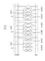
- FIG. 6 is a circuit diagram of a demultiplexer according to an exemplary embodiment of the present invention, which can be employed in the organic electroluminescent display of FIG. 3;
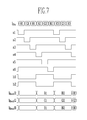
- FIG. 7 is a timing diagram of input and output signals of the demultiplexer of FIG. 6;
- FIG. 8 is a circuit diagram of a demultiplexer using a 1:2 demultiplexing circuit.
- FIG. 9 is a view showing a sample/hold circuit of FIG. 6.
- the display device can be an organic electroluminescent display, for example.
- FIG. 3 is a circuit diagram of an organic electroluminescent display having an active matrix of n ⁇ m pixels according to an exemplary embodiment of the present invention.
- an organic electroluminescent display includes a panel 21, a scan driver 22, a data driver 23, and a demultiplexer 24.
- the panel 21 includes n ⁇ m pixels 25; n first scan lines SCAN1[1], SCAN1[2], ..., SCAN1[n], which are horizontally formed; n second scan lines SCAN2[1], SCAN2[2], ..., SCAN2[n], which are respectively arranged in parallel with n first scan lines; and 3m output data lines DoutR[1], DoutG[1], DoutB[1], ..., DoutR[m], DoutG[m], DoutB[m], where n and m are natural numbers.
- each pixel 25 includes three sub-pixels 26R, 26G, 26B, that is, a red sub-pixel 26R, a green sub-pixel 26G, and a blue sub-pixel 26B.
- the first and second scan lines SCAN1, SCAN2 (e.g., one of the first scan lines SCAN1[1] to SCAN1[n] and one of the second scan lines SCAN2[1] to SCAN2[n]) respectively transmit first and second scan signals to the pixel 25.
- the red, green and blue output data lines DoutR, DoutG, DoutB respectively transmit output data currents to the red, green, blue sub-pixels 26R, 26G, 26B.
- the sub-pixels 26R, 26G, 26B are operated by a current programming method. That is, a capacitor (e.g., a capacitor C' of FIG.
- the scan driver 22 transmits the first and second scan signals to the first and second scan lines SCAN1, SCAN2.
- the data driver 23 transmits input data currents to m input data lines Din[1], Din[2],.. Din[m].
- the demultiplexer 24 receives the input data currents and demultiplexes them into output data currents, thereby transmitting the output data currents to 3m output data lines DoutR[1], DoutG[1], DoutB[1], ..., DoutR[m], DoutG[m], DoutB[m].
- the demultiplexer 24 includes m sample/hold type demultiplexing circuits, examples of which are shown in FIG. 6. Each demultiplexing circuit is a 1:3 demultiplexing circuit, so that the input data current transmitted to one input data line Din is demultiplexed and transmitted to three output data lines DoutR, DoutG, DoutB.
- FIG. 4 is a circuit diagram of a sub-pixel employed in the organic electroluminescent display of FIG. 3.
- SCAN1 represents one of the first scan lines SCAN1[1] to SCAN1[n] of FIG. 3
- SCAN2 represents one of the second scan lines SCAN2[1] to SCAN2[n].
- Dout represents one of the data lines DoutR[1], DoutG[1], DoutB[1], ..., DoutR[m], DoutG[m], DoutB[m] of FIG. 3.
- a sub-pixel includes an organic light emitting device OLED and a sub-pixel circuit.
- the sub-pixel circuit includes a driving transistor MD'; first, second, third switching transistors MS1, MS2, MS3; and a capacitor C'.
- Each of the driving transistor MD', the first, second, and third switching transistors MS1, MS2, MS3 includes a gate, a source and a drain.
- the capacitor C' includes a first terminal and a second terminal.
- the first switching transistor MS1 includes the gate connected to the first scan line SCAN1, the source connected to a first node N1, and the drain connected to the output data line Dout.
- the output data line Dout is one of the red, green and blue output data lines illustrated in FIG. 3.
- the first switching transistor MS1 charges the capacitor C' in response to the first scan signal of the first scan line SCAN1.
- the second switching transistor MS2 includes the gate connected to the first scan line SCAN1, the source connected to a second node N2, and the drain connected to the output data line Dout.
- the second switching transistor MS2 transmits the output data current I Dout flowing in the output data line Dout to the driving transistor MD' in response to the first scan signal of the first scan line SCAN1.
- the third switching transistor MS3 includes the gate connected to the second scan line SCAN2, the source connected to the second node N2, and the drain connected to the organic light emitting device OLED.
- the third switching transistor MS3 transmits a current flowing through the driving transistor MD' to the organic light emitting device OLED in response to the second scan signal of the second scan line SCAN2.
- the capacitor C' includes the first terminal to which the power voltage V DD is applied, and the second terminal connected to the first node N1. While the first and second switching transistors MS1, MS2 are turned on, the capacitor C' is charged corresponding to voltage V GS between the gate and the source according to the output data current I Dout flowing in the driving transistor MD'. On the other hand, while the first and second switching transistors MS1, MS2 are turned off, the capacitor C' substantially maintains the voltage V GS .
- the driving transistor MD' includes the gate connected to the first node N1, the source to which the power voltage V DD is applied, and the drain connected to the second node N2. While the third switching transistor MS3 is turned on, the driving transistor MD' supplies a current to the organic light emitting device OLED, wherein the current corresponds to the voltage applied between the first and second terminals of the capacitor C'.
- FIG. 5 is a timing diagram of signals for driving the sub-pixel of FIG. 4, wherein the signals include first and second scan signals scan1, scan 2.
- the third switching transistor MS3 is turned on and the first and second switching transistors MS1, MS2 are turned off. Because the electric charge charged in the capacitor C' for the selection period is maintained for the light emission period, the voltage between the first and second terminals of the capacitor C' is determined for the selection period, that is, the voltage V GS between the gate and the source of the driving transistor MD' is maintained for the light emission period.
- the current I OLED flowing in the organic light emitting device OLED of the sub-pixel shown in FIG. 4 is equal to the output data current I Dout , so that the current I OLED flowing in the organic light emitting device OLED is not affected by a threshold voltage V TH and a gain factor ⁇ of the driving transistor MD', thereby realizing the organic electroluminescent display improved in uniformity of brightness.
- FIG. 6 is a circuit diagram of a demultiplexer according to an exemplary embodiment of the present invention, which can be employed in the organic electroluminescent display of FIG. 3, for example.
- the demultiplexer includes m demultiplexing circuits 31.
- Each demultiplexing circuit 31 includes a sample/hold type 1:3 demultiplexing circuit 31, so that the input data current transmitted to one input data line Din (e.g., one of Din[1] to Din[m]) is demultiplexed and transmitted to three output data lines DoutR (e.g., one of DoutR[1] to DoutR[m]), DoutG (e.g., one of DoutG[1] to DoutG[m]), DoutB (e.g., one of DoutB[1] to DoutB[m]).
- Each demultiplexing circuit 31 includes first through sixth sample/hold circuits S/H1 ⁇ S/H6.
- the first through sixth sample lines S1 ⁇ S6 and the first and second hold lines H1, H2 are connected to each demultiplexing circuit 31.
- the first sample/hold circuit S/H1 records a voltage corresponding to a current transmitted to the input data line Din in a capacitor (e.g., a capacitor C hold of FIG. 9) in response to a first sampling signal of the first sample line S1, and then transmits a current corresponding to the voltage recorded in the capacitor to the red output data line DoutR in response to a first hold signal of the first hold line H1.
- a capacitor e.g., a capacitor C hold of FIG. 9
- the second sample/hold circuit S/H2 records a voltage corresponding to a current transmitted to the input data line Din in a capacitor (e.g., as shown in FIG. 9) in response to a second sampling signal of the second sample line S2, and then transmits a current corresponding to the voltage recorded in the capacitor to the green output data line DoutG in response to the first holding signal of the first hold line H1.
- the third sample/hold circuit S/H3 records a voltage corresponding to a current transmitted to the input data line Din in a capacitor (e.g., as shown in FIG. 9) in response to a third sampling signal of the third sample line S3, and then transmits a current corresponding to the voltage recorded in the capacitor to the blue output data line DoutB in response to the first holding signal of the first hold line H1.
- the fourth sample/hold circuit S/H4 records a voltage corresponding to a current transmitted to the input data line Din in a capacitor (e.g., as shown in FIG. 9) in response to a fourth sampling signal of the fourth sample line S4, and then transmits a current corresponding to the voltage recorded in the capacitor to the red output data line DoutR in response to a second holding signal of the second hold line H2.
- the fifth sample/hold circuit S/H5 records a voltage corresponding to a current transmitted to the input data line Din in a capacitor (e.g., as shown in FIG. 9) in response to a fifth sampling signal of the fifth sample line S5, and then transmits a current corresponding to the voltage recorded in the capacitor to the green output data line DoutG in response to the second holding signal of the second hold line H2.
- the sixth sample/hold circuit S/H6 records a voltage corresponding to a current transmitted to the input data line Din in a capacitor (e.g., as shown in FIG. 9) in response to a sixth sampling signal of the sixth sample line S6, and then transmits a current corresponding to the voltage recorded in the capacitor to the blue output data line DoutB in response to the second holding signal of the second hold line H2.
- FIG. 7 is a timing diagram of input and output signals of the demultiplexer of FIG. 6.
- FIG. 7 illustrates an input data current I Din ; first through sixth sampling signals s1, s2, ..., s6; first and second holding signals h1, h2; and red, green, blue output data currents I Dout R, I Dout G, I Dout B.
- the demultiplexing circuit 31 operates as follows. Since each of the demultiplexing circuits 31 operates in substantially the same manner, the description of operation will be given below in reference to the demultiplexing circuit 31 connected to the output data lines DoutR[1], DoutG[1] and DoutB [1] only.
- a current R1 of the input data current I Din is sampled and stored in the first sample/hold circuit S/H1.
- a current G1 of the input data current I Din is sampled and stored in the second sample/hold circuit S/H2.
- a current B1 of the input data current I Din is sampled and stored in the third sample/hold circuit S/H3.
- a current R2 of the input data current I Din is sampled and stored in the fourth sample/hold circuit S/H4.
- a current G2 of the input data current I Din is sampled and stored in the fifth sample/hold circuit S/H5.
- a current B2 of the input data current I Din is sampled and stored in the fourth sample/hold circuit S/H6.
- the first holding signal h1 is high, so that the first through third sample/hold circuits S/H1, S/H2, SH3 receive the first holding signal h1 and supply currents corresponding to the sampled currents R1, G1, B1 to the output data lines DoutR[1], DoutG[1], DoutB[1], respectively.
- a current R3 of the input data current I Din is sampled and stored in the first sample/hold circuit S/H1.
- a current G3 of the input data current I Din is sampled and stored in the second sample/hold circuit S/H2.
- a current B3 of the input data current I Din is sampled and stored in the third sample/hold circuit S/H3.
- the second holding signal h2 is high, so that the fourth through sixth sample/hold circuits S/H4, S/H5, SH6 receive the second holding signal h2 and supply currents corresponding to the sampled currents R2, G2, B2 to the output data lines DoutR[1], DoutG[1], DoutB[1], respectively.
- the sample/hold type demultiplexing circuit 31 demultiplexes the current inputted to the input data line Din[1] and transmits them to the output data lines DoutR[1], DoutG[1], DoutB[1].
- the first through third sample/hold circuits S/H1, S/H2, S/H3 included in the demultiplexing circuit 31 may receive and sample the input data current I Din having the same magnitude and output output data currents I Dout R, I Dout G, I Dout B that are different from each other.
- the reason for this is as follows.
- the first sample/hold circuit S/H1 outputs the output data currents I Dout R after a lapse of a predetermined period after the input data current I Din is sampled, so that the capacitor storing the voltage corresponding to the input data current I Din is discharged, thereby allowing the output data current I Dout R to be lower than the input data current I Din .
- the third sample/hold circuit S/H3 sends the output data current I Dout B almost immediately after sampling the input data current I Din , so that little electric discharge occurs in the capacitor and the third sample/hold circuit S/H3 sends the output data current I Dout B, which is higher than that of the first sample/hold circuit S/H1 after they have received and sampled the input data current I Din having the same magnitude.
- the second sample/hold circuit S/H2 outputs the output data current I Dout G, which is higher than that of the first sample/hold circuit S/H1 and lower than that of the third sample/hold circuit S/H3.
- the first through third sample/hold circuits S/H1, S/H2, S/H3 can output the output data currents I Dout R, I Dout G, I Dout B that are different from each other after receiving and sampling the input data current I Din having the same magnitude.
- the fourth through sixth sample/hold circuits S/H4, S/H5, S/H6 output the output data currents I Dout R, I Dout G, I Dout B that are different from each other after receiving the input data current I Din having the same magnitude.
- the output data currents I Dout R, I Dout G, I Dout B transmitted to the respective data lines are different from each other, so that a vertical pattern may normally develop on the panel of the organic electroluminescent display.
- the demultiplexing circuit 31 is a 1:3 demultiplexing circuit, the vertical pattern would typically not result. That is, the differences in the output data currents I Dout R, I Dout G, I Dout B are caused among the first through third sample/hold circuits S/H1, S/H2, S/H3 provided in the demultiplexing circuit 31, so that only a set ratio among red, green and blue is changed in color coordinates, i.e., the color just changed. Further, all demultiplexing circuits 31 of the demultiplexer have substantially the same characteristics and substantially the same change in color. Therefore, the entire panel of the organic electroluminescent display is changed in color and has little vertical pattern. The change in color can be compensated by resetting the color coordinates of the data driver, for example.
- FIG. 8 illustrates the demultiplexer including 1:2 demultiplexing circuits 32.
- a first red output data line DoutR[1] and a first green output data line DoutG[1] are connected to a first demultiplexing circuit.
- a first blue output data line DoutB[1] is connected to a second demultiplexing circuit.
- a second red output data line DoutR[2] is connected to the second demultiplexing circuit.
- a second green output data line DoutG[2] and a second blue output data line DoutB[2] are connected to a third demultiplexing circuit.
- each demultiplexing circuit 32 when the first sample/hold circuit S/H1 outputs the output data current higher than that of the second sample/hold circuit S/H2 after receiving the input data current having the same magnitude, the output data current of the first green output data line DoutG[1] is lower than those of the first red and blue output data lines DoutR[1] and DoutB[1], so that the green color is relatively dark. At this time, the output data current of the second green output data line DoutG[2] is higher than those of the second red and blue output data lines DoutR[2] and DoutB[2], so that the green color is relatively bright. Therefore, the brightness difference in color causes the panel of the organic electroluminescent display to have a vertical pattern. Such a pattern arises in a 1:4 demultiplexing circuit, a 1:5 demultiplexing circuit, etc.
- k is a natural number
- y is the number of sub-pixels included in each pixel.
- y is 3.
- y is 4.
- the vertical pattern generally does not arise when the number of output data lines connected to each demultiplexing circuit is equal to an integer multiple of the number of sub-pixels included in each pixel, such as is the case of the demultiplexer in FIG. 6.
- a vertical pattern typically arises when the number of output data lines connected to each demultiplexing circuit is not equal to an integer multiple of the number of sub-pixels included in each pixel, such as is the case of the demultiplexer in FIG. 8.
- the first and fourth sample/hold circuits S/H1, S/H4 of the demultiplexing circuit 31 can output different output data currents I Dout R after sampling the input data current I Din having the same magnitude.
- the cause of the different output data currents I Dout R is as follows.
- the first and the fourth sample/hold circuits S/H1 and S/H4 have different parasitic capacitor connections (i.e., different parasitic capacitance) due to difference in circuit connections or circuit layouts thereof, so that the output data currents I Dout R can be different from each other after sampling the input data current I Din having the same magnitude.
- the second and fifth sample/hold circuits S/H2, S/H5 can output different output data currents I Dout G after sampling the input data current I Din having the same magnitude.
- the third and the sixth sample/hold circuits S/H3, S/H6 can output different output data currents I Dout B after sampling the input data current I Din having the same magnitude. Accordingly, a horizontal pattern may arise or develop on the panel of the organic electroluminescent display. That is, when the first sample/hold circuit S/H1 outputs the output data current I Dout R higher than that of the fourth sample/hold circuit S/H4, the odd numbered lines of a frame has relatively high brightness, but even numbered lines of the frame has relatively low brightness, so that the horizontal pattern may arise on the panel.
- Such a horizontal pattern can be reduced or eliminated as follows.
- the first sample/hold circuit S/H1 outputs the output data current I Dout R to the odd numbered lines
- the fourth sample/hold circuit S/H4 outputs the output data current I Dout R to the even numbered lines.
- the first sample/hold circuit S/H1 outputs the output data current I Dout R to the even numbered lines
- the fourth sample/hold circuit S/H4 outputs the output data current I Dout R to the odd numbered lines.
- FIG. 9 is a view showing one of the sample/hold circuits 31 of FIG. 6.
- the sample/hold circuits can have other configurations in other embodiments.
- a sample/hold circuit includes first through fifth switches SW1, SW2, ..., SW5; a first transistor M1; and a hold capacitor C hold ⁇
- the first switch SW1 electrically connects an input data line Din with a drain of the first transistor M1 in response to a sampling signal s.
- the second switch SW2 electrically connects a source of the first transistor M1 with a high voltage line V DD in response to the sampling signal s.
- the third switch SW3 electrically connects the input data line Din with a second terminal of the hold capacitor C hold in response to the sampling signal s.
- the fourth switch SW4 electrically connects an output data line Dout with the source of the first transistor M1 in response to a holding signal h.
- the fifth switch SW5 electrically connects the drain of the first transistor M1 with a low voltage line V SS in response to the holding signal h.
- the hold capacitor C hold has a first terminal connected to the source of the first transistor M1, and the second terminal connected to a gate of the first transistor M1.
- the sample/hold circuit allows the hold capacitor C hold to record a voltage corresponding to the input data current I Din in response to the sampling signal s, and transmits the current corresponding to the voltage recorded in the hold capacitor C hold to the output data line in response to the holding signal h.
- An output terminal of the data driver should be a current sink type where an external current is flown into the data driver through the output terminal.
- the data driver having a current sink type output terminal decreases deviation in output current, requires a relatively low voltage level in its power supply, and reduces the cost of a chip for the data driver.
- the sample/hold circuit shown in FIG. 9 has a current source type input terminal adapted to the current sink type output terminal of the data driver. That is, the current flows outwardly through the input terminal of the sample/hold circuit.
- the present invention provides an organic electroluminescent display and a demultiplexer, in which a data driver has a simple structure and a stationary pattern due to demultiplexing is eliminated.
Landscapes
- Engineering & Computer Science (AREA)
- Physics & Mathematics (AREA)
- Computer Hardware Design (AREA)
- General Physics & Mathematics (AREA)
- Theoretical Computer Science (AREA)
- Electroluminescent Light Sources (AREA)
- Control Of Indicators Other Than Cathode Ray Tubes (AREA)
- Control Of El Displays (AREA)
- Measurement And Recording Of Electrical Phenomena And Electrical Characteristics Of The Living Body (AREA)
- Measuring Pulse, Heart Rate, Blood Pressure Or Blood Flow (AREA)
- Auxiliary Devices For Music (AREA)
Abstract
Description
Claims (19)
- A display device comprising:wherein at least one of the demultiplexing circuits demultiplexes a corresponding one of the second data currents transmitted from one of the second data lines into at least two of the first data currents, and transmits the at least two of the first data currents to at least two of the first data lines, wherein a number of the at least two of the first data lines is an integer multiple of a number of the sub-pixels in each of the pixels.a plurality of pixels, each comprising a plurality of sub-pixels;a plurality of scan lines through which scan signals are applied to the plurality of pixels;a plurality of first data lines through which first data currents are transmitted to the plurality of pixels;a scan driver for outputting the scan signals to the plurality of scan lines;a demultiplexer comprising a plurality of demultiplexing circuits for demultiplexing second data currents into the first data currents, and for transmitting the first data currents to the plurality of first data lines; anda data driver for transmitting the second data currents to the demultiplexer through a plurality of second data lines,
- The display device according to claim 1, wherein each of the pixels comprises three sub-pixels consisting of a red sub-pixel, a green sub-pixel, and a blue sub-pixel.
- The display device according to claim 1, wherein each of the pixels comprises four sub-pixels consisting of a red sub-pixel, a green sub-pixel, a blue sub-pixel, and a white sub-pixel.
- The display device according to claim 1, wherein the plurality of scan lines comprise a plurality of first scan lines and a plurality of second scan lines, and the scan signals comprise first scan signals and second scan signals, and
wherein each of the sub-pixels comprises an organic light emitting device, first, second and third switching transistors, a driving transistor, and a capacitor. - The display device according to claim 4, wherein the first scan signals of the first scan lines and the second scan signals of the second scan lines include periodic signals, wherein one period of each of the first and second scan signals includes a selection period and a light emission period,
wherein a corresponding one of the first scan signals turns on the first and second switching transistors during the selection period, and turns off the first and second switching transistors during the light emission period, and
wherein a corresponding one of the second scan signals turns off the third switching transistor during the selection period, and turns on the third switching transistor during the light emission period. - The display device according to claim 4, wherein the first switching transistor charges the capacitor with electric charges in response to a corresponding one of the first scan signals,
wherein the second switching transistor transmits one of the at least two of the first data currents flowing in one of the at least two of the first data lines to the driving transistor in response to the corresponding one of the first scan signals,
wherein the third switching transistor transmits a current flowing in the driving transistor to the organic light emitting device in response to a corresponding one of the second scan signals,
wherein the capacitor is charged with the electric charges corresponding to a voltage, which corresponds to the current flowing in the driving transistor, applied between a gate and a source of the driving transistor for a period when the first and second switching transistors are turned on, and maintains the voltage for another period when the first and second switching transistors are turned off, and
wherein the driving transistor supplies the current, which corresponds to the voltage applied between first and second terminal of the capacitor, to the organic light emitting device for a period when the third switching transistor is turned on. - The display device according to claim 6, wherein the first scan signals of the first scan lines and the second scan signals of the second scan lines include periodic signals, and one period of each of the first and second scan signals includes a selection period and a light emission period,
wherein a corresponding one of the first scan signals turns on the first and second switching transistors during the selection period, and turns off the first and second switching transistors during the light emission period, and
wherein a corresponding one of the second scan signals turns off the third switching transistor during the selection period, and turns on the third switching transistor during the light emission period. - The display device according to claim 4, wherein the first switching transistor comprises a gate connected to a corresponding one of the first scan lines, a source connected to a first node, and a drain connected to one of the at least two of the first data lines,
wherein the second switching transistor comprises a gate connected to the corresponding one of the first scan lines, a source connected to a second node, and a drain connected to the one of the at least two of the first data lines,
wherein the third switching transistor comprises a gate connected to a corresponding one of the second scan lines, a source connected to the second node, and a drain connected to the organic light emitting device,
wherein the capacitor comprises a first terminal to which a power voltage is applied, and a second terminal connected to the first node, and
wherein the driving transistor comprises a gate connected to the first node, a source to which the power voltage is applied, and a drain connected to the second node. - The display device according to claim 8, wherein the first scan signals of the first scan lines and the second scan signals of the second scan lines include periodic signals, and one period of each of the first and second scan signals includes a selection period and a light emission period,
wherein a corresponding one of the first scan signals turns on the first and second switching transistors during the selection period, and turns off the first and second switching transistors during the light emission period, and
wherein a corresponding one of the second scan signals turns off the third switching transistor during the selection period, and turns on the third switching transistor during the light emission period. - The display device according to claim 1, wherein at least one of the demultiplexing circuits comprises:first and second group sample/hold circuits, each group sample/hold circuit comprising a plurality of sample/hold circuits,wherein a number of the sample/hold circuits in each of the first and second group sample/hold circuits is an integer multiple of the number of the sub-pixels in each of the pixels, andthe second group sample/hold circuit outputs at least one of the at least two of the first data currents corresponding to at least one previously sampled said corresponding one of the second data currents while the first group sample/hold circuit samples the corresponding one of the second data currents, and the first group sample/hold circuit outputs at least one of the at least two of the first data currents corresponding to at least another previously sampled said corresponding one of the second data currents while the second group sample/hold circuit samples the corresponding one of the second data currents.
- The display device according to claim 10, wherein the first group sample/hold circuit alternately outputs one of the at least two of the first data currents to the pixels of odd numbered lines and even numbered lines as frames are changed, and
wherein the second group sample/hold circuit alternately outputs another one of the at least two of the first data currents to the pixels of the odd numbered lines and the even numbered lines as the frames are changed. - The display device according to claim 10, wherein at least one of the sample/hold circuits comprises:a first transistor having a source, a drain and a gate;a hold capacitor having a first terminal connected to the source of the first transistor, and a second terminal connected to the gate of the first transistor;a first switch for connecting the one of the second data lines to the drain of the first transistor in response to a sampling signal;a second switch for connecting the source of the first transistor to a high voltage line in response to the sampling signal;a third switch for connecting the one of the second data lines to the second terminal of the hold capacitor in response to the sampling signal;a fourth switch for connecting one of the at least two of the first data lines to the source of the first transistor in response to a holding signal; anda fifth switch for connecting the drain of the first transistor to a low voltage line in response to the holding signal.
- The display device according to claim 12, wherein the sampling signal and the holding signal include periodic signals, and one period of each of the sampling and holding signals includes a sampling period and a holding period,
wherein the sampling signal turns on the first, second and third switches during the sampling period, and turns off the first, second and third switches during the holding period, and
wherein the holding signal turns off the fourth and fifth switches during the sampling period, and turns on the fourth and fifth switches during the holding period. - A demultiplexer comprising:wherein at least one of the demultiplexing circuits demultiplexes a corresponding one of the second data currents transmitted from a second data line into at least two of the first data currents in response to the sampling and holding signals, and transmits the at least two of the first data currents to at least two first data lines, wherein a number of the at least two first data lines is an integer multiple of a number of the sub-pixels in each of the pixels.a plurality of demultiplexing circuits for transmitting first data currents to a plurality of pixels, each pixel comprising a plurality of sub-pixels;a plurality of sample signal lines through which sampling signals are transmitted to the demultiplexing circuits, wherein a number of sampling signal lines is an integer multiple of a number of the sub-pixels included in each of the pixels; andfirst and second hold signal lines through which holding signals are transmitted to the demultiplexing circuits,
- The demultiplexer according to claim 14, wherein each of the pixels comprises three sub-pixels consisting of a red sub-pixel, a green sub-pixel, and a blue sub-pixel.
- The demultiplexer according to claim 14, wherein each of the pixels comprises four sub-pixels consisting of a red sub-pixel, a green sub-pixel, a blue sub-pixel, and a white sub-pixel.
- The demultiplexer according to claim 14, wherein at least one of the demultiplexing circuits comprises:wherein a number of the sample/hold circuits in each of the first and second group sample/hold circuits is an integer multiple of the number of the sub-pixels in each of the pixels, andfirst and second group sample/hold circuits, each group sample/hold circuit comprising a plurality of sample/hold circuits,
wherein the second group sample/hold circuit outputs at least one of the at least two of the first data currents corresponding to at least one previously sampled said corresponding one of the second data currents while the first group sample/hold circuit samples the corresponding one of the second data currents, and the first group sample/hold circuit outputs at least one of the at least two of the first data currents corresponding to at least another previously sampled said corresponding one of the second data currents while the second group sample/hold circuit samples the corresponding one of the second data currents. - The demultiplexer according to claim 17, wherein at least one of the sample/hold circuits comprises:a first transistor having a source, a drain and a gate;a hold capacitor having a first terminal connected to the source of the first transistor, and a second terminal connected to the gate of the first transistor;a first switch for connecting the second data line to the drain of the first transistor in response to a corresponding one of the sampling signals;a second switch for connecting the source of the first transistor to a high voltage line in response to the corresponding one of the sampling signals;a third switch for connecting the second data line to the second terminal of the hold capacitor in response to the corresponding one of the sampling signals;a fourth switch for connecting one of the at least two of the first data lines to the source of the first transistor in response to a corresponding one of the holding signals; anda fifth switch for connecting the drain of the first transistor to a low voltage line in response to the corresponding one of the holding signals.
- The demultiplexer according to claim 18, wherein the sampling signals and the holding signals each include periodic signals, and one period of each of the sampling and holding signals includes a sampling period and a holding period;
wherein the sampling signal turns on the first, second and third switches during the sampling period, and turns off the first, second and third switches during the holding period; and
wherein the holding signal turns off the fourth and fifth switches during the sampling period, and turns on the fourth and fifth switches during the holding period.
Applications Claiming Priority (2)
| Application Number | Priority Date | Filing Date | Title |
|---|---|---|---|
| KR1020040034560A KR100600350B1 (en) | 2004-05-15 | 2004-05-15 | Demultiplexing and organic electroluminescent display device having same |
| KR2004034560 | 2004-05-15 |
Publications (2)
| Publication Number | Publication Date |
|---|---|
| EP1596358A1 true EP1596358A1 (en) | 2005-11-16 |
| EP1596358B1 EP1596358B1 (en) | 2009-04-01 |
Family
ID=34939750
Family Applications (1)
| Application Number | Title | Priority Date | Filing Date |
|---|---|---|---|
| EP05103845A Expired - Lifetime EP1596358B1 (en) | 2004-05-15 | 2005-05-10 | Display device and demultiplexer |
Country Status (7)
| Country | Link |
|---|---|
| US (1) | US7692673B2 (en) |
| EP (1) | EP1596358B1 (en) |
| JP (1) | JP2006047973A (en) |
| KR (1) | KR100600350B1 (en) |
| CN (1) | CN100409282C (en) |
| AT (1) | ATE427544T1 (en) |
| DE (1) | DE602005013600D1 (en) |
Cited By (1)
| Publication number | Priority date | Publication date | Assignee | Title |
|---|---|---|---|---|
| CN113176809A (en) * | 2021-04-12 | 2021-07-27 | 维沃移动通信有限公司 | Electronic device |
Families Citing this family (29)
| Publication number | Priority date | Publication date | Assignee | Title |
|---|---|---|---|---|
| KR100581799B1 (en) * | 2004-06-02 | 2006-05-23 | 삼성에스디아이 주식회사 | Organic electroluminescent display device and demultiplexer |
| TWI275056B (en) * | 2005-04-18 | 2007-03-01 | Wintek Corp | Data multiplex circuit and its control method |
| KR101213937B1 (en) * | 2005-04-18 | 2012-12-18 | 엘지디스플레이 주식회사 | Electro-luminescence display device |
| US20070063192A1 (en) * | 2005-09-20 | 2007-03-22 | Toppoly Optoelectronics Corp. | Systems for emitting light incorporating pixel structures of organic light-emitting diodes |
| KR100732824B1 (en) * | 2005-12-02 | 2007-06-27 | 삼성에스디아이 주식회사 | OLED display and driving method thereof |
| KR100732853B1 (en) * | 2006-02-28 | 2007-06-27 | 삼성에스디아이 주식회사 | Pixel and organic light emitting display device using same |
| JP4281765B2 (en) * | 2006-08-09 | 2009-06-17 | セイコーエプソン株式会社 | Active matrix light emitting device, electronic device, and pixel driving method for active matrix light emitting device |
| US7875840B2 (en) * | 2006-11-16 | 2011-01-25 | Aptina Imaging Corporation | Imager device with anti-fuse pixels and recessed color filter array |
| US7593248B2 (en) * | 2006-11-16 | 2009-09-22 | Aptina Imaging Corporation | Method, apparatus and system providing a one-time programmable memory device |
| KR100897171B1 (en) | 2007-07-27 | 2009-05-14 | 삼성모바일디스플레이주식회사 | Organic light emitting display |
| KR101416904B1 (en) * | 2007-11-07 | 2014-07-09 | 엘지디스플레이 주식회사 | Driving apparatus for organic electro-luminescence display device |
| JP4930501B2 (en) | 2008-12-22 | 2012-05-16 | ソニー株式会社 | Display device and electronic device |
| KR101150163B1 (en) * | 2009-10-30 | 2012-05-25 | 주식회사 실리콘웍스 | Circuit and method for driving organic light emitting diode display |
| TWI557711B (en) * | 2011-05-12 | 2016-11-11 | 半導體能源研究所股份有限公司 | Display device driving method |
| KR101986657B1 (en) * | 2011-11-09 | 2019-06-10 | 엘지디스플레이 주식회사 | Organic light emitting diode display device and method of driving the same |
| KR102092703B1 (en) * | 2012-05-18 | 2020-03-25 | 삼성디스플레이 주식회사 | Display device and the method for repairing the display device |
| KR102022387B1 (en) * | 2012-12-05 | 2019-09-19 | 삼성디스플레이 주식회사 | Organic light emitting diplay and method for operating the same |
| KR102137079B1 (en) * | 2014-03-03 | 2020-07-24 | 삼성디스플레이 주식회사 | Organic light emitting display device |
| CN103943082B (en) | 2014-03-25 | 2016-03-16 | 京东方科技集团股份有限公司 | A kind of display device and driving method thereof |
| KR102325675B1 (en) * | 2014-12-29 | 2021-11-12 | 삼성디스플레이 주식회사 | Organic Light Emitting Display Device |
| KR102325659B1 (en) * | 2014-12-29 | 2021-11-12 | 삼성디스플레이 주식회사 | Organic Light Emitting Display Device |
| TWI555000B (en) | 2015-02-05 | 2016-10-21 | 友達光電股份有限公司 | Display panel |
| CN104835451B (en) * | 2015-05-22 | 2017-07-18 | 京东方科技集团股份有限公司 | A kind of display base plate, display device and its driving method |
| CN106935217B (en) * | 2017-03-23 | 2019-03-15 | 武汉华星光电技术有限公司 | Multiple-channel output selection circuit and display device |
| US20190041676A1 (en) * | 2017-08-02 | 2019-02-07 | Wuhan China Star Optoelectronics Technology Co., Ltd. | A lcd panel and a driving circuit for the lcd panel |
| KR102633408B1 (en) * | 2018-09-12 | 2024-02-06 | 엘지디스플레이 주식회사 | Display Device and Driving Method Thereof |
| CN110910845A (en) * | 2019-11-18 | 2020-03-24 | 福建华佳彩有限公司 | Dot display driving method |
| KR20220161903A (en) * | 2021-05-31 | 2022-12-07 | 엘지디스플레이 주식회사 | Display panel, display device including the display panel and personal immersion system using the display device |
| CN117275428B (en) * | 2023-10-11 | 2025-12-19 | 上海天马微电子有限公司 | Display panel and display device |
Citations (3)
| Publication number | Priority date | Publication date | Assignee | Title |
|---|---|---|---|---|
| US6333729B1 (en) * | 1997-07-10 | 2001-12-25 | Lg Electronics Inc. | Liquid crystal display |
| US20030132907A1 (en) * | 2002-01-14 | 2003-07-17 | Lg. Philips Lcd Co., Ltd. | Apparatus and method for driving liquid crystal display |
| US20030179164A1 (en) * | 2002-03-21 | 2003-09-25 | Dong-Yong Shin | Display and a driving method thereof |
Family Cites Families (70)
| Publication number | Priority date | Publication date | Assignee | Title |
|---|---|---|---|---|
| JPS57201295A (en) * | 1981-06-04 | 1982-12-09 | Sony Corp | Two-dimensional address device |
| JPH0754420B2 (en) * | 1989-05-22 | 1995-06-07 | 日本電気株式会社 | Driving method for liquid crystal display device |
| JPH06118913A (en) * | 1992-08-10 | 1994-04-28 | Casio Comput Co Ltd | Liquid crystal display |
| US5426447A (en) * | 1992-11-04 | 1995-06-20 | Yuen Foong Yu H.K. Co., Ltd. | Data driving circuit for LCD display |
| US5510807A (en) * | 1993-01-05 | 1996-04-23 | Yuen Foong Yu H.K. Co., Ltd. | Data driver circuit and associated method for use with scanned LCD video display |
| JPH06337400A (en) * | 1993-05-31 | 1994-12-06 | Sharp Corp | Matrix-type display device and driving method |
| US5555001A (en) * | 1994-03-08 | 1996-09-10 | Prime View Hk Limited | Redundant scheme for LCD display with integrated data driving circuit |
| US5633653A (en) * | 1994-08-31 | 1997-05-27 | David Sarnoff Research Center, Inc. | Simultaneous sampling of demultiplexed data and driving of an LCD pixel array with ping-pong effect |
| JP3110980B2 (en) * | 1995-07-18 | 2000-11-20 | インターナショナル・ビジネス・マシーンズ・コーポレ−ション | Driving device and method for liquid crystal display device |
| FR2743658B1 (en) * | 1996-01-11 | 1998-02-13 | Thomson Lcd | METHOD FOR ADDRESSING A FLAT SCREEN USING A PRECHARGE OF THE PIXELS CONTROL CIRCUIT ALLOWING THE IMPLEMENTATION OF THE METHOD AND ITS APPLICATION TO LARGE DIMENSION SCREENS |
| JPH10260661A (en) * | 1997-03-19 | 1998-09-29 | Sharp Corp | Display device drive circuit |
| KR100239413B1 (en) * | 1997-10-14 | 2000-01-15 | 김영환 | Driving device of liquid crystal display device |
| JP5240884B2 (en) | 1998-05-16 | 2013-07-17 | トムソン ライセンシング | Driving device for display device arranged in bus |
| US6348906B1 (en) * | 1998-09-03 | 2002-02-19 | Sarnoff Corporation | Line scanning circuit for a dual-mode display |
| TW530287B (en) * | 1998-09-03 | 2003-05-01 | Samsung Electronics Co Ltd | Display device, and apparatus and method for driving display device |
| JP2000105574A (en) * | 1998-09-29 | 2000-04-11 | Matsushita Electric Ind Co Ltd | Current control type light emitting device |
| JP3800831B2 (en) | 1998-10-13 | 2006-07-26 | セイコーエプソン株式会社 | Display device and electronic device |
| KR100430100B1 (en) * | 1999-03-06 | 2004-05-03 | 엘지.필립스 엘시디 주식회사 | Driving Method of Liquid Crystal Display |
| KR100701892B1 (en) * | 1999-05-21 | 2007-03-30 | 엘지.필립스 엘시디 주식회사 | Data line driving method and liquid crystal display device using the same |
| JP2001195042A (en) * | 2000-01-05 | 2001-07-19 | Internatl Business Mach Corp <Ibm> | Source driver for liquid crystal panel and leveling method for source driver output variance |
| JP4831872B2 (en) * | 2000-02-22 | 2011-12-07 | 株式会社半導体エネルギー研究所 | Image display device drive circuit, image display device, and electronic apparatus |
| US6781600B2 (en) * | 2000-04-14 | 2004-08-24 | Picsel Technologies Limited | Shape processor |
| JP4593740B2 (en) | 2000-07-28 | 2010-12-08 | ルネサスエレクトロニクス株式会社 | Display device |
| JP2002162934A (en) * | 2000-09-29 | 2002-06-07 | Eastman Kodak Co | Flat-panel display with luminance feedback |
| JP2003195815A (en) * | 2000-11-07 | 2003-07-09 | Sony Corp | Active matrix type display device and active matrix type organic electroluminescence display device |
| US7015882B2 (en) * | 2000-11-07 | 2006-03-21 | Sony Corporation | Active matrix display and active matrix organic electroluminescence display |
| JP4929431B2 (en) * | 2000-11-10 | 2012-05-09 | Nltテクノロジー株式会社 | Data line drive circuit for panel display device |
| JP4155389B2 (en) | 2001-03-22 | 2008-09-24 | 株式会社半導体エネルギー研究所 | LIGHT EMITTING DEVICE, ITS DRIVE METHOD, AND ELECTRONIC DEVICE |
| JP3579368B2 (en) * | 2001-05-09 | 2004-10-20 | 三洋電機株式会社 | Drive circuit and display device |
| US6667580B2 (en) * | 2001-07-06 | 2003-12-23 | Lg Electronics Inc. | Circuit and method for driving display of current driven type |
| JP3951687B2 (en) * | 2001-08-02 | 2007-08-01 | セイコーエプソン株式会社 | Driving data lines used to control unit circuits |
| JP2003058108A (en) | 2001-08-22 | 2003-02-28 | Sony Corp | Color display device and color organic electroluminescence display device |
| JP4193452B2 (en) | 2001-08-29 | 2008-12-10 | 日本電気株式会社 | Semiconductor device for driving current load device and current load device having the same |
| US7256756B2 (en) * | 2001-08-29 | 2007-08-14 | Nec Corporation | Semiconductor device for driving a current load device and a current load device provided therewith |
| JP4650601B2 (en) | 2001-09-05 | 2011-03-16 | 日本電気株式会社 | Current drive element drive circuit, drive method, and image display apparatus |
| US7259740B2 (en) * | 2001-10-03 | 2007-08-21 | Nec Corporation | Display device and semiconductor device |
| JP3890948B2 (en) | 2001-10-17 | 2007-03-07 | ソニー株式会社 | Display device |
| JP3601499B2 (en) * | 2001-10-17 | 2004-12-15 | ソニー株式会社 | Display device |
| TWI261217B (en) * | 2001-10-31 | 2006-09-01 | Semiconductor Energy Lab | Driving circuit of signal line and light emitting apparatus |
| TWI256607B (en) * | 2001-10-31 | 2006-06-11 | Semiconductor Energy Lab | Signal line drive circuit and light emitting device |
| US7006072B2 (en) | 2001-11-10 | 2006-02-28 | Lg.Philips Lcd Co., Ltd. | Apparatus and method for data-driving liquid crystal display |
| JP2003157048A (en) * | 2001-11-19 | 2003-05-30 | Matsushita Electric Ind Co Ltd | Active matrix display |
| JP3982249B2 (en) | 2001-12-11 | 2007-09-26 | 株式会社日立製作所 | Display device |
| JP3637911B2 (en) | 2002-04-24 | 2005-04-13 | セイコーエプソン株式会社 | Electronic device, electronic apparatus, and driving method of electronic device |
| CN1666242A (en) * | 2002-04-26 | 2005-09-07 | 东芝松下显示技术有限公司 | Driving Circuit for Electroluminescence Display |
| JP4490650B2 (en) | 2002-04-26 | 2010-06-30 | 東芝モバイルディスプレイ株式会社 | EL display device driving method and EL display device |
| KR100956463B1 (en) * | 2002-04-26 | 2010-05-10 | 도시바 모바일 디스플레이 가부시키가이샤 | EL display |
| JP4165120B2 (en) | 2002-05-17 | 2008-10-15 | 株式会社日立製作所 | Image display device |
| JP3970110B2 (en) | 2002-06-27 | 2007-09-05 | カシオ計算機株式会社 | CURRENT DRIVE DEVICE, ITS DRIVE METHOD, AND DISPLAY DEVICE USING CURRENT DRIVE DEVICE |
| US20040056852A1 (en) * | 2002-09-23 | 2004-03-25 | Jun-Ren Shih | Source driver for driver-on-panel systems |
| JP4103544B2 (en) | 2002-10-28 | 2008-06-18 | セイコーエプソン株式会社 | Organic EL device |
| WO2004047067A1 (en) * | 2002-11-20 | 2004-06-03 | Mitsubishi Denki Kabushiki Kaisha | Image display apparatus |
| US8035626B2 (en) * | 2002-11-29 | 2011-10-11 | Semiconductor Energy Laboratory Co., Ltd. | Current driving circuit and display device using the current driving circuit |
| KR100894643B1 (en) * | 2002-12-03 | 2009-04-24 | 엘지디스플레이 주식회사 | Data driving device and method of liquid crystal display |
| JP4663327B2 (en) | 2003-02-28 | 2011-04-06 | 株式会社半導体エネルギー研究所 | Semiconductor device |
| US6771028B1 (en) * | 2003-04-30 | 2004-08-03 | Eastman Kodak Company | Drive circuitry for four-color organic light-emitting device |
| KR100515299B1 (en) * | 2003-04-30 | 2005-09-15 | 삼성에스디아이 주식회사 | Image display and display panel and driving method of thereof |
| JP3671973B2 (en) * | 2003-07-18 | 2005-07-13 | セイコーエプソン株式会社 | Display driver, display device, and driving method |
| JP4595300B2 (en) | 2003-08-21 | 2010-12-08 | セイコーエプソン株式会社 | Electro-optical device and electronic apparatus |
| KR100529076B1 (en) | 2003-11-10 | 2005-11-15 | 삼성에스디아이 주식회사 | Demultiplexer, and display apparatus using the same |
| KR100529075B1 (en) * | 2003-11-10 | 2005-11-15 | 삼성에스디아이 주식회사 | Demultiplexer using current sample/hold circuit, and display apparatus using the same |
| KR100578911B1 (en) * | 2003-11-26 | 2006-05-11 | 삼성에스디아이 주식회사 | Current demultiplexing device and current write type display device using the same |
| KR100589381B1 (en) * | 2003-11-27 | 2006-06-14 | 삼성에스디아이 주식회사 | Display device using demultiplexer and driving method thereof |
| KR100578914B1 (en) | 2003-11-27 | 2006-05-11 | 삼성에스디아이 주식회사 | Display device using demultiplexer |
| KR100649244B1 (en) * | 2003-11-27 | 2006-11-24 | 삼성에스디아이 주식회사 | Demultiplexing device and display device using same |
| KR100589376B1 (en) | 2003-11-27 | 2006-06-14 | 삼성에스디아이 주식회사 | Light emitting display device using demultiplexer |
| KR100578913B1 (en) | 2003-11-27 | 2006-05-11 | 삼성에스디아이 주식회사 | Display device using demultiplexer and driving method thereof |
| KR100622217B1 (en) * | 2004-05-25 | 2006-09-08 | 삼성에스디아이 주식회사 | Organic electroluminescent display and demultiplexer |
| KR100581799B1 (en) * | 2004-06-02 | 2006-05-23 | 삼성에스디아이 주식회사 | Organic electroluminescent display device and demultiplexer |
| KR101469033B1 (en) * | 2008-01-08 | 2014-12-04 | 삼성디스플레이 주식회사 | Liquid crystal display and control method thereof |
-
2004
- 2004-05-15 KR KR1020040034560A patent/KR100600350B1/en not_active Expired - Fee Related
-
2005
- 2005-04-06 JP JP2005109586A patent/JP2006047973A/en active Pending
- 2005-05-09 US US11/124,926 patent/US7692673B2/en active Active
- 2005-05-10 AT AT05103845T patent/ATE427544T1/en not_active IP Right Cessation
- 2005-05-10 DE DE602005013600T patent/DE602005013600D1/en not_active Expired - Lifetime
- 2005-05-10 EP EP05103845A patent/EP1596358B1/en not_active Expired - Lifetime
- 2005-05-11 CN CNB2005100702185A patent/CN100409282C/en not_active Expired - Fee Related
Patent Citations (3)
| Publication number | Priority date | Publication date | Assignee | Title |
|---|---|---|---|---|
| US6333729B1 (en) * | 1997-07-10 | 2001-12-25 | Lg Electronics Inc. | Liquid crystal display |
| US20030132907A1 (en) * | 2002-01-14 | 2003-07-17 | Lg. Philips Lcd Co., Ltd. | Apparatus and method for driving liquid crystal display |
| US20030179164A1 (en) * | 2002-03-21 | 2003-09-25 | Dong-Yong Shin | Display and a driving method thereof |
Non-Patent Citations (2)
| Title |
|---|
| KRETZ T ET AL: "22.3: A 3.4-inch Reflective Colour Active Matrix Liquid Crystal Display without Polarisers", SID, vol. XXXIII, May 2002 (2002-05-01), pages 798, XP007007962 * |
| MASUYUKI OHTA ET AL: "9.4: A Novel Current Programmed Pixel for Active Matrix OLED Displays", SID, vol. XXXIV, 20 May 2003 (2003-05-20), pages 108, XP007008209 * |
Cited By (2)
| Publication number | Priority date | Publication date | Assignee | Title |
|---|---|---|---|---|
| CN113176809A (en) * | 2021-04-12 | 2021-07-27 | 维沃移动通信有限公司 | Electronic device |
| CN113176809B (en) * | 2021-04-12 | 2024-05-03 | 维沃移动通信有限公司 | Electronic equipment |
Also Published As
| Publication number | Publication date |
|---|---|
| CN1697006A (en) | 2005-11-16 |
| ATE427544T1 (en) | 2009-04-15 |
| KR100600350B1 (en) | 2006-07-14 |
| US20050259052A1 (en) | 2005-11-24 |
| DE602005013600D1 (en) | 2009-05-14 |
| JP2006047973A (en) | 2006-02-16 |
| CN100409282C (en) | 2008-08-06 |
| EP1596358B1 (en) | 2009-04-01 |
| US7692673B2 (en) | 2010-04-06 |
| KR20050109372A (en) | 2005-11-21 |
Similar Documents
| Publication | Publication Date | Title |
|---|---|---|
| US7692673B2 (en) | Display device and demultiplexer | |
| US7782277B2 (en) | Display device having demultiplexer | |
| US7742021B2 (en) | Organic electroluminescent display and demultiplexer | |
| US8018401B2 (en) | Organic electroluminescent display and demultiplexer | |
| KR100589972B1 (en) | Electro optical device, driving method of electro optical device and electronic apparatus | |
| US7224303B2 (en) | Data driving apparatus in a current driving type display device | |
| US6873116B2 (en) | Light emitting device | |
| KR20010014615A (en) | An active electro-luminescence display device | |
| US11727889B2 (en) | Display device | |
| US7330162B2 (en) | Method of driving a light emitting device and electronic equipment | |
| US10270462B2 (en) | Digital analog conversion circuit, data driver, display device, electronic apparatus and driving method of digital analog conversion circuit, driving method of data driver, and driving method of display device | |
| US8427403B2 (en) | Demultiplexer, display apparatus using the same, and display panel thereof | |
| US20040207617A1 (en) | Display circuit | |
| US20100085388A1 (en) | Active matrix display device | |
| US20060221016A1 (en) | Display | |
| KR100646995B1 (en) | OLED display and demultiplexer with precharge | |
| US20060290612A1 (en) | Current sample-and-hold circuit and display device including the same | |
| KR100671821B1 (en) | Organic led display |
Legal Events
| Date | Code | Title | Description |
|---|---|---|---|
| PUAI | Public reference made under article 153(3) epc to a published international application that has entered the european phase |
Free format text: ORIGINAL CODE: 0009012 |
|
| 17P | Request for examination filed |
Effective date: 20050606 |
|
| AK | Designated contracting states |
Kind code of ref document: A1 Designated state(s): AT BE BG CH CY CZ DE DK EE ES FI FR GB GR HU IE IS IT LI LT LU MC NL PL PT RO SE SI SK TR |
|
| AX | Request for extension of the european patent |
Extension state: AL BA HR LV MK YU |
|
| AKX | Designation fees paid |
Designated state(s): AT BE BG CH CY CZ DE DK EE ES FI FR GB GR HU IE IS IT LI LT LU MC NL PL PT RO SE SI SK TR |
|
| 17Q | First examination report despatched |
Effective date: 20060215 |
|
| GRAP | Despatch of communication of intention to grant a patent |
Free format text: ORIGINAL CODE: EPIDOSNIGR1 |
|
| GRAS | Grant fee paid |
Free format text: ORIGINAL CODE: EPIDOSNIGR3 |
|
| RAP1 | Party data changed (applicant data changed or rights of an application transferred) |
Owner name: SAMSUNG MOBILE DISPLAY CO., LTD. |
|
| GRAA | (expected) grant |
Free format text: ORIGINAL CODE: 0009210 |
|
| AK | Designated contracting states |
Kind code of ref document: B1 Designated state(s): AT BE BG CH CY CZ DE DK EE ES FI FR GB GR HU IE IS IT LI LT LU MC NL PL PT RO SE SI SK TR |
|
| REG | Reference to a national code |
Ref country code: GB Ref legal event code: FG4D |
|
| REG | Reference to a national code |
Ref country code: CH Ref legal event code: EP |
|
| REG | Reference to a national code |
Ref country code: IE Ref legal event code: FG4D |
|
| REF | Corresponds to: |
Ref document number: 602005013600 Country of ref document: DE Date of ref document: 20090514 Kind code of ref document: P |
|
| PG25 | Lapsed in a contracting state [announced via postgrant information from national office to epo] |
Ref country code: SI Free format text: LAPSE BECAUSE OF FAILURE TO SUBMIT A TRANSLATION OF THE DESCRIPTION OR TO PAY THE FEE WITHIN THE PRESCRIBED TIME-LIMIT Effective date: 20090401 |
|
| NLV1 | Nl: lapsed or annulled due to failure to fulfill the requirements of art. 29p and 29m of the patents act | ||
| PG25 | Lapsed in a contracting state [announced via postgrant information from national office to epo] |
Ref country code: FI Free format text: LAPSE BECAUSE OF FAILURE TO SUBMIT A TRANSLATION OF THE DESCRIPTION OR TO PAY THE FEE WITHIN THE PRESCRIBED TIME-LIMIT Effective date: 20090401 Ref country code: LT Free format text: LAPSE BECAUSE OF FAILURE TO SUBMIT A TRANSLATION OF THE DESCRIPTION OR TO PAY THE FEE WITHIN THE PRESCRIBED TIME-LIMIT Effective date: 20090401 Ref country code: EE Free format text: LAPSE BECAUSE OF FAILURE TO SUBMIT A TRANSLATION OF THE DESCRIPTION OR TO PAY THE FEE WITHIN THE PRESCRIBED TIME-LIMIT Effective date: 20090401 Ref country code: PT Free format text: LAPSE BECAUSE OF FAILURE TO SUBMIT A TRANSLATION OF THE DESCRIPTION OR TO PAY THE FEE WITHIN THE PRESCRIBED TIME-LIMIT Effective date: 20090902 Ref country code: ES Free format text: LAPSE BECAUSE OF FAILURE TO SUBMIT A TRANSLATION OF THE DESCRIPTION OR TO PAY THE FEE WITHIN THE PRESCRIBED TIME-LIMIT Effective date: 20090712 Ref country code: AT Free format text: LAPSE BECAUSE OF FAILURE TO SUBMIT A TRANSLATION OF THE DESCRIPTION OR TO PAY THE FEE WITHIN THE PRESCRIBED TIME-LIMIT Effective date: 20090401 |
|
| PG25 | Lapsed in a contracting state [announced via postgrant information from national office to epo] |
Ref country code: PL Free format text: LAPSE BECAUSE OF FAILURE TO SUBMIT A TRANSLATION OF THE DESCRIPTION OR TO PAY THE FEE WITHIN THE PRESCRIBED TIME-LIMIT Effective date: 20090401 Ref country code: IS Free format text: LAPSE BECAUSE OF FAILURE TO SUBMIT A TRANSLATION OF THE DESCRIPTION OR TO PAY THE FEE WITHIN THE PRESCRIBED TIME-LIMIT Effective date: 20090801 Ref country code: SE Free format text: LAPSE BECAUSE OF FAILURE TO SUBMIT A TRANSLATION OF THE DESCRIPTION OR TO PAY THE FEE WITHIN THE PRESCRIBED TIME-LIMIT Effective date: 20090701 Ref country code: NL Free format text: LAPSE BECAUSE OF FAILURE TO SUBMIT A TRANSLATION OF THE DESCRIPTION OR TO PAY THE FEE WITHIN THE PRESCRIBED TIME-LIMIT Effective date: 20090401 |
|
| PG25 | Lapsed in a contracting state [announced via postgrant information from national office to epo] |
Ref country code: MC Free format text: LAPSE BECAUSE OF NON-PAYMENT OF DUE FEES Effective date: 20090531 |
|
| REG | Reference to a national code |
Ref country code: CH Ref legal event code: PL |
|
| PG25 | Lapsed in a contracting state [announced via postgrant information from national office to epo] |
Ref country code: DK Free format text: LAPSE BECAUSE OF FAILURE TO SUBMIT A TRANSLATION OF THE DESCRIPTION OR TO PAY THE FEE WITHIN THE PRESCRIBED TIME-LIMIT Effective date: 20090401 Ref country code: CH Free format text: LAPSE BECAUSE OF NON-PAYMENT OF DUE FEES Effective date: 20090531 Ref country code: LI Free format text: LAPSE BECAUSE OF NON-PAYMENT OF DUE FEES Effective date: 20090531 Ref country code: RO Free format text: LAPSE BECAUSE OF FAILURE TO SUBMIT A TRANSLATION OF THE DESCRIPTION OR TO PAY THE FEE WITHIN THE PRESCRIBED TIME-LIMIT Effective date: 20090401 Ref country code: CZ Free format text: LAPSE BECAUSE OF FAILURE TO SUBMIT A TRANSLATION OF THE DESCRIPTION OR TO PAY THE FEE WITHIN THE PRESCRIBED TIME-LIMIT Effective date: 20090401 |
|
| PLBE | No opposition filed within time limit |
Free format text: ORIGINAL CODE: 0009261 |
|
| STAA | Information on the status of an ep patent application or granted ep patent |
Free format text: STATUS: NO OPPOSITION FILED WITHIN TIME LIMIT |
|
| PG25 | Lapsed in a contracting state [announced via postgrant information from national office to epo] |
Ref country code: SK Free format text: LAPSE BECAUSE OF FAILURE TO SUBMIT A TRANSLATION OF THE DESCRIPTION OR TO PAY THE FEE WITHIN THE PRESCRIBED TIME-LIMIT Effective date: 20090401 Ref country code: BE Free format text: LAPSE BECAUSE OF FAILURE TO SUBMIT A TRANSLATION OF THE DESCRIPTION OR TO PAY THE FEE WITHIN THE PRESCRIBED TIME-LIMIT Effective date: 20090401 |
|
| 26N | No opposition filed |
Effective date: 20100105 |
|
| PG25 | Lapsed in a contracting state [announced via postgrant information from national office to epo] |
Ref country code: BG Free format text: LAPSE BECAUSE OF FAILURE TO SUBMIT A TRANSLATION OF THE DESCRIPTION OR TO PAY THE FEE WITHIN THE PRESCRIBED TIME-LIMIT Effective date: 20090701 |
|
| PG25 | Lapsed in a contracting state [announced via postgrant information from national office to epo] |
Ref country code: IE Free format text: LAPSE BECAUSE OF NON-PAYMENT OF DUE FEES Effective date: 20090510 |
|
| PG25 | Lapsed in a contracting state [announced via postgrant information from national office to epo] |
Ref country code: GR Free format text: LAPSE BECAUSE OF FAILURE TO SUBMIT A TRANSLATION OF THE DESCRIPTION OR TO PAY THE FEE WITHIN THE PRESCRIBED TIME-LIMIT Effective date: 20090702 |
|
| PG25 | Lapsed in a contracting state [announced via postgrant information from national office to epo] |
Ref country code: IT Free format text: LAPSE BECAUSE OF FAILURE TO SUBMIT A TRANSLATION OF THE DESCRIPTION OR TO PAY THE FEE WITHIN THE PRESCRIBED TIME-LIMIT Effective date: 20090401 |
|
| PG25 | Lapsed in a contracting state [announced via postgrant information from national office to epo] |
Ref country code: LU Free format text: LAPSE BECAUSE OF NON-PAYMENT OF DUE FEES Effective date: 20090510 |
|
| PG25 | Lapsed in a contracting state [announced via postgrant information from national office to epo] |
Ref country code: HU Free format text: LAPSE BECAUSE OF FAILURE TO SUBMIT A TRANSLATION OF THE DESCRIPTION OR TO PAY THE FEE WITHIN THE PRESCRIBED TIME-LIMIT Effective date: 20091002 |
|
| PG25 | Lapsed in a contracting state [announced via postgrant information from national office to epo] |
Ref country code: TR Free format text: LAPSE BECAUSE OF FAILURE TO SUBMIT A TRANSLATION OF THE DESCRIPTION OR TO PAY THE FEE WITHIN THE PRESCRIBED TIME-LIMIT Effective date: 20090401 |
|
| PG25 | Lapsed in a contracting state [announced via postgrant information from national office to epo] |
Ref country code: CY Free format text: LAPSE BECAUSE OF FAILURE TO SUBMIT A TRANSLATION OF THE DESCRIPTION OR TO PAY THE FEE WITHIN THE PRESCRIBED TIME-LIMIT Effective date: 20090401 |
|
| REG | Reference to a national code |
Ref country code: GB Ref legal event code: 732E Free format text: REGISTERED BETWEEN 20130103 AND 20130109 |
|
| REG | Reference to a national code |
Ref country code: DE Ref legal event code: R082 Ref document number: 602005013600 Country of ref document: DE Representative=s name: GULDE HENGELHAUPT ZIEBIG & SCHNEIDER, DE |
|
| REG | Reference to a national code |
Ref country code: DE Ref legal event code: R082 Ref document number: 602005013600 Country of ref document: DE Representative=s name: GULDE HENGELHAUPT ZIEBIG & SCHNEIDER, DE Effective date: 20130416 Ref country code: DE Ref legal event code: R081 Ref document number: 602005013600 Country of ref document: DE Owner name: SAMSUNG DISPLAY CO., LTD., KR Free format text: FORMER OWNER: SAMSUNG MOBILE DISPLAY CO. LTD., SUWON, KR Effective date: 20130416 Ref country code: DE Ref legal event code: R082 Ref document number: 602005013600 Country of ref document: DE Representative=s name: GULDE & PARTNER PATENT- UND RECHTSANWALTSKANZL, DE Effective date: 20130416 Ref country code: DE Ref legal event code: R081 Ref document number: 602005013600 Country of ref document: DE Owner name: SAMSUNG DISPLAY CO., LTD., YONGIN-CITY, KR Free format text: FORMER OWNER: SAMSUNG MOBILE DISPLAY CO. LTD., SUWON, GYEONGGI, KR Effective date: 20130416 |
|
| REG | Reference to a national code |
Ref country code: FR Ref legal event code: PLFP Year of fee payment: 12 |
|
| PGFP | Annual fee paid to national office [announced via postgrant information from national office to epo] |
Ref country code: GB Payment date: 20160511 Year of fee payment: 12 Ref country code: DE Payment date: 20160511 Year of fee payment: 12 |
|
| PGFP | Annual fee paid to national office [announced via postgrant information from national office to epo] |
Ref country code: FR Payment date: 20160512 Year of fee payment: 12 |
|
| REG | Reference to a national code |
Ref country code: DE Ref legal event code: R119 Ref document number: 602005013600 Country of ref document: DE |
|
| GBPC | Gb: european patent ceased through non-payment of renewal fee |
Effective date: 20170510 |
|
| REG | Reference to a national code |
Ref country code: FR Ref legal event code: ST Effective date: 20180131 |
|
| PG25 | Lapsed in a contracting state [announced via postgrant information from national office to epo] |
Ref country code: GB Free format text: LAPSE BECAUSE OF NON-PAYMENT OF DUE FEES Effective date: 20170510 Ref country code: DE Free format text: LAPSE BECAUSE OF NON-PAYMENT OF DUE FEES Effective date: 20171201 |
|
| PG25 | Lapsed in a contracting state [announced via postgrant information from national office to epo] |
Ref country code: FR Free format text: LAPSE BECAUSE OF NON-PAYMENT OF DUE FEES Effective date: 20170531 |