EP1596307A1 - I/O configuration messaging within a link-based computing system - Google Patents
I/O configuration messaging within a link-based computing system Download PDFInfo
- Publication number
- EP1596307A1 EP1596307A1 EP04255078A EP04255078A EP1596307A1 EP 1596307 A1 EP1596307 A1 EP 1596307A1 EP 04255078 A EP04255078 A EP 04255078A EP 04255078 A EP04255078 A EP 04255078A EP 1596307 A1 EP1596307 A1 EP 1596307A1
- Authority
- EP
- European Patent Office
- Prior art keywords
- segment
- configuration
- link
- component
- computing system
- Prior art date
- Legal status (The legal status is an assumption and is not a legal conclusion. Google has not performed a legal analysis and makes no representation as to the accuracy of the status listed.)
- Granted
Links
Images



Classifications
-
- G—PHYSICS
- G06—COMPUTING OR CALCULATING; COUNTING
- G06F—ELECTRIC DIGITAL DATA PROCESSING
- G06F13/00—Interconnection of, or transfer of information or other signals between, memories, input/output devices or central processing units
- G06F13/38—Information transfer, e.g. on bus
- G06F13/40—Bus structure
- G06F13/4004—Coupling between buses
- G06F13/4022—Coupling between buses using switching circuits, e.g. switching matrix, connection or expansion network
-
- G—PHYSICS
- G06—COMPUTING OR CALCULATING; COUNTING
- G06F—ELECTRIC DIGITAL DATA PROCESSING
- G06F13/00—Interconnection of, or transfer of information or other signals between, memories, input/output devices or central processing units
- G06F13/38—Information transfer, e.g. on bus
Definitions
- the field of invention relates generally to computing systems; and, more specifically, to I/O configuration messaging within a link-based computing system.
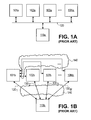
- FIG. 1a shows a depiction of a bus 120.
- a bus 120 is a "shared medium" communication structure that is used to transport communications between electronic components 101a - 10Na and 110a.
- Shared medium means that the components 101 a - 10Na and 110a that communicate with one another physically share and are connected to the same electronic wiring 120. That is, wiring 120 is a shared resource that is used by any of components 101 a - 10Na and 110a to communicate with any other of components 101 a - 10Na and 110a.
- component 101 a wished to communicate to component 10Na, component 101 a would send information along wiring 120 to component 10Na; if component 103a wished to communicate to component 110a, component 103a would send information along the same wiring 120 to component 110a, etc.
- bus 120 corresponds to a PCI bus where components 101a - 10Na correspond to "I/O" components (e.g., LAN networking adapter cards, MODEMs, hard disk storage devices, etc.) and component 110a corresponds to an I/O Control Hub (ICH).
- I/O I/O Control Hub
- bus 120 corresponds to a "front side" bus where components 101 a - 10Na correspond to microprocessors and component 110a corresponds to a memory controller.
- busses are less and less practical as computing system speeds grow. Basically, as the capacitive loading of any wiring increases, the maximum speed at which that wiring can transport information decreases. That is, there is an inverse relationship between a wiring's capacitive loading and that same wiring's speed. Each component that is added to a wire causes that wire's capacitive loading to grow. Thus, because busses typically couple multiple components, bus wiring 120 is typically regarded as being heavily loaded with capacitance.
- FIG. 1b shows a comparative example vis-à-vis Figure 1a.
- computing system components 101 a - 10Na and 110a are interconnected through a network 140 of high speed bi-directional point-to-point links 130 1 through 130 N .
- a bi-directional point-to-point link typically comprises a first unidirectional point-to-point link that transmits information in a first direction and a second unidirectional point-to-point link that transmits information is a second direction that is opposite that of the first direction. Because a unidirectional point-to-point link typically has a single endpoint, its capacitive loading is substantially less than that of a shared media bus.
- Each point-to-point link can be constructed with copper or fiber optic cabling and appropriate drivers and receivers (e.g., single or differential line drivers and receivers for copper based cables; and LASER or LED E/O transmitters and O/E receivers for fiber optic cables;, etc.).
- the network 140 observed in Figure 1b is simplistic in that each component is connected by a point-to-point link to every other component.
- the network 140 includes routing/switching nodes.
- every component need not be coupled by a point-to-point link to every other component Instead, hops across a plurality of links may take place through routing/switching nodes in order to transport information from a source component to a destination component.
- the routing/switching function may be a stand alone function within the network or may be integrated into a substantive component of the computing system (e.g., processor, memory controller, I/O unit, etc.).
- FIG. 2 shows an embodiment of a link-based I/O segment 200.
- An I/O segment is a region of circuitry within a computing system that permits I/O units to exchange information between one another and/or between other components of a computing system outside the I/O segment.
- a computing system's I/O units can be viewed as those portions of a computing system's functionality responsible for receiving information from outside the computing system and/or for sending information from inside the computing system to outside the computing system. Therefore, I/O units typically includes user interfaces (e.g., a keyboard interface, a mouse interface, a display interface), network interfaces (e.g., a MODEM, a wireless LAN adapter, etc.) and printer interfaces.
- user interfaces e.g., a keyboard interface, a mouse interface, a display interface
- network interfaces e.g., a MODEM, a wireless LAN adapter, etc.
- I/O is viewed from the perspective of the computing system's processor(s) and system memory rather than the entire computing system as a whole. From this perspective, I/O is viewed as that portion of the computing system's functionality that can send information at least to and/or from the computing system's system memory.
- non-volatile storage devices such as disk storage devices (e.g., magnetic disc drive, CD ROM, etc.) and/or "flash cards" are often included in the list of a computing system's I/O units (along with the I/O units mentioned above). The later perspective of I/O is used by this application unless otherwise indicated.
- the link-based I/O segment of Figure 2 is consistent with a PCI Express I/O segment.
- PCI Express is an industry standard I/O segment architecture.
- the PCI Express I/O architecture of Figure 2 connects each of I/O units 205 1-5 through its own bi-directional link. Any two of I/O units 205 2-5 can send information between each other through switch 202.
- Switch 202 also supports communication between any one of I/O units 205 2-5 and the rest of the computing system.
- a legacy bus 207 (e.g., a PCI bus) is also observed that uses a bridge 204 connected through a bi-directional link to a root complex 201.
- An I/O segment may comprise an access point through which information between the I/O segment and the rest of the computing system flows (note that the root complex 201 is the access point for the I/O segment 200 of Figure 2).
- I/O segments often are designed to receive and respond to configuration commands 208 at an access point of the I/O segment.
- configuration commands 208 can typically be targeted for a particular I/O unit in order to configure some functional aspect of the I/O unit's behavior.
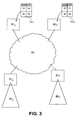
- Figures 3 and 4 together present a design that ensures the proper routing of an I/O configuration transaction packet to the correct target I/O segment within a link-based computing system having a plurality of I/O segments.
- a link-based computing system (or a portion thereof) is shown.
- the link-based computing system includes four components 301 1 through 301 4 .
- Components 301 1 and 301 3 each have (not shown in Figure 3 for illustrative ease) at least one processor configured to execute software that performs I/O segment configuration tasks.
- Components 301 2 and 301 4 at least behave as gateways for the access point of I/O segments 300 1 and 300 2 , respectively. As such, configuration transaction packets directed to I/O segment 300 1 should be sent to component 301 2 and configuration transaction packets directed to I/O segment 300 2 should be sent to component 301 4 .
- Network 340 is the network of the link-based computing system. During operation, either of components 301 1 or 301 3 may seek to initiate a configuration transaction to an I/O unit associated with either one of I/O segments 300 1 and 300 2 . At least two types of configuration transactions exist: 1) a write; and, 2) a read.
- a packet is sent from the component executing the configuration software (e.g., one of components 301 1 and 301 3 ) to the I/O segment that the I/O unit that is targeted for the read is connected into.
- the packet in order to send a packet to the targeted I/O unit, the packet should be routed over the network 340 to the gateway component for the access point of the targeted I/O segment.
- the packet includes content (e.g., in the packet payload) that among other possible items of information: 1) identifies the target I/O unit; and, 2) identifies the register within the target I/O from which information is to be read.
- the I/O segment that the targeted I/O unit is connected into understands the packet's content and reads the information from the identified register within the identified target I/O unit.
- the register information that was read from the I/O unit is then placed into the payload of a second packet that is sent over network 340 to the component that initiated the transaction.
- a packet is sent from the component executing the configuration software (e.g., one of components 301 1 and 301 3 ) to the I/O segment that the I/O unit that is targeted for the write is connected into.
- the packet includes content that among other possible items of information: 1) identifies the target I/O unit; 2) identifies the register within the target I/O to which information is to be written; and, 3) the information to be written into the identified register.
- the I/O segment that the targeted I/O unit is connected into understands the packet's content and writes the information into the identified register within the identified target I/O unit.
- a response e.g., indicating a successful write
- Transactions executed over a network 340 in link-based computing systems may be made identified with an address. That is, for example, each specific type of transaction may be given a unique address which is executed on the component that initiates the transaction. In order to initiate a specific transaction, the transaction's address is decoded by the component's hardware into the actions needed to perform the transaction.
- a configuration read transaction as address that corresponds to a configuration read transaction is decoded by the hardware of the component that initiates the transaction into the actions of sending a packet to the targeted I/O segment having content to be interpreted by the targeted I/O segment as a read.
- address that corresponds to a configuration write transaction is decoded by the hardware of the component that initiates the transaction into the actions of sending a packet to the targeted I/O segment having content to be interpreted by the targeted I/O segment as a write.
- Figure 3 indicates, by way of memory maps 313 1 and 313 2 , that a memory mapped source address decoding process may be used to produce the routing information sufficient to route the initial transaction packet to the gateway component for the targeted I/O segment. According to the memory maps 313 1 and 313 2 of Figures 3 , a different address range is used for each I/O segment to be targeted.
- each of memory maps 313 1 and 313 2 have a first address range (R1) for those configuration transaction addresses that are targeted for I/O segment 300 1 and a second address range (R2) for those configuration transaction addresses that are targeted for I/O segment 300 2 .
- R1 range of map 313 1 may be a different range of physical address space than the R1 range of map 313 2 .
- R2 range of map 313 1 may be a different range of physical address space than the R1 range of map 313 2 .
- the memory devices used to implement memory maps 313 1 and 313 2 may include random access memory (RAM) and/or content addressable memory (CAM). In the case of CAMs,the R1 and R2 ranges may corresponds to key ranges rather than address ranges.
- Figures 4 and 5 elaborate on an embodiment of the transaction address decoding process in more detail.
- Figure 4 shows a high level hardware design for circuitry within a component 401 of a link-based computing system that can emit configuration packets destined for the correct one amongst a plurality of I/O segments; and, Figure 5 shows a methodology that could be executed by the hardware design of Figure 4.
- a configuration transaction address 405, 505 is initially generated 501.
- the configuration transaction address 405, 505 is generated 501 by I/O configuration software whose purpose is to control the configuration of I/O units dispersed across more than one I/O segment within a link-based computing system.
- the specific embodiment of Figure 5 indicates that the configuration transaction address 505 includes the following data structure: Segment/Bus/Device/Function/Extended_Reg/Reg.
- Bus/Device/Function/Extended_Reg/Reg portion 505a of the configuration transaction address 505 as the standard format for a PCI, PCI-X or PCl_Express configuration transaction.
- the "Bus” parameter identifies which PCI bus (in the case, PCI, PCI-X and PCl_Express) or PCl_Express link (in the case of PCl_Express) within the I/O segment is targeted for the configuration transaction.
- the "Device” parameter identifies which I/O unit on the targeted bus/link is targeted for the configuration transaction.
- the "Function” parameter identifies the function to be performed by the configuration transaction (e.g., read or write).
- the "Extended_Reg" (if available) and "Reg” parameters define the register space of the targeted I/O unit to be affected by the configuration transaction.
- the Segment parameter 505a is a novel feature that identifies which I/O segment within the link based computing system is targeted by the configuration transaction. Note that the entire configuration transaction may include more information/parameters than the just the Segment/Bus/Device/Function/Extended_Reg/Reg structure 505. For purposes of identifying a memory mapped address decoding process that is sufficient for identifying a target I/O unit connected to any one of a plurality of I/O segments within a link-based computing system, however, only the Segment/Bus/Device/Function/Extended_Reg/Reg portion 505 of the transaction address needs to be shown.
- the Segment parameter 505b in identifying the targeted I/O segment for the transaction, serves as an input parameter to a source address decoder 402 that determines the specific network node (NodelD) of the gateway component for the targeted I/O segment (e:g., referring to Figure 3, component 301 2 if I/O segment 300 1 is the targeted I/O segment; or, component 301 4 if I/O segment 300 2 is the targeted I/O segment).
- the source address decoder 414 includes look up logic circuitry 414 for looking up NodelD information from memory map 413 in response to being presented with the portion 405a of the configuration transaction address 405 (specifically, the Segment parameter 505a).
- the NodelD of the gateway component to the targeted I/O segment is provided as an output of the source address decoder 402.
- the configuration transaction addressing space may be partitioned so that a first address range is reserved for configuration transaction addresses whose corresponding configuration transactions all target the same "first" I/O segment (e.g., I/O segment 300 1 ); a second address range is reserved for configuration transaction addresses whose corresponding configuration transactions all target the same "second" I/O segment (e.g., I/O segment 300 2 ), etc.
- a plurality of parallel source address decoders are implemented to improve performance (i.e., improve the number of look-ups per second).
- a first source address decoder is used to identify the NodelD for a first gateway component and a second address decoder is used to identify the NodelD for a second gateway component.
- the NodelD output 406 is combined with the rest of the information 405b needed to fully characterize the configuration transaction (e.g., the Bus/Device/Function/Extended_Reg/Reg portion 505b) at the networking layer 403 of the component 401.
- the networking layer 403 is responsible for creating and sending a packet 503 over the link-based computing system's network 440.
- Figure 5 also illustrates a depiction of an exemplary packet 504 that is produced by the networking layer 403; where, the packet corresponds to a situation where component 301 1 of Figure 3 sends a configuration transaction packet over network 340 to component 301 2 for purposes of executing a configuration function upon an I/O unit connected to I/O segment 300 1 .
- the payload of the packet 504b includes the Bus/Device/Function/Extended_Reg/Reg portion 505b portion of the configuration transaction address 505. The payload portion would also include the information to be written in the case of a write transaction.
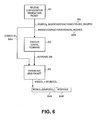
- Figure 6 shows a methodology that can be executed at the gateway component in response to its receipt 601 of a configuration transaction address.
- the methodology of Figure 6 refers to the specific embodiment referred to just above where component 301 1 of Figure 3 sends a configuration transaction packet over network 340 to component 301 2 for purposes of executing a configuration function upon an I/O unit connected to I/O-segment 300 1 .
- the methodology of Figure 6 corresponds to the behavior of component 301 2 in response to its receipt 601 of packet 504 sent from component 301 1 .
- Pertinent information 605 for purposes of explaining the response is observed in Figure 6 as including the SourcelD 1 (which identifies component 301 1 ) and the Bus/Device/Function/Extended_Reg/Reg information.
- the Bus/Device/Function/Extended_Reg/Reg information 605b is understood by and used by the I/O segment 300 1 that is accessed through the gateway component 301 2 .
- the I/O segment executes 602 the function of the configuration transaction that it specifies.
- the response 606 depends upon the function. For example, in the case of a read transaction, the response would be the information read from the targeted register. In the case of a write transaction, the response might include an affirmation that the write operation was carried out successfully.
- NodelD specifies the identity of the destination component for a packet
- the SourcelD specifies the identity of the sending component for the packet
- the SourcelD for the response packet is the identity of the gateway component (i.e., SourcelD 2 ).
- the header 604a of the response packet is NodelD 1 /SourcelD 2 .
- the payload 604b of the response packet is the response 606 from the executed configuration function.
Landscapes
- Engineering & Computer Science (AREA)
- Theoretical Computer Science (AREA)
- Physics & Mathematics (AREA)
- General Engineering & Computer Science (AREA)
- General Physics & Mathematics (AREA)
- Mathematical Physics (AREA)
- Computer Hardware Design (AREA)
- Data Exchanges In Wide-Area Networks (AREA)
- Computer And Data Communications (AREA)
- Multi Processors (AREA)
- Information Transfer Systems (AREA)
- Small-Scale Networks (AREA)
Abstract
Description
- The field of invention relates generally to computing systems; and, more specifically, to I/O configuration messaging within a link-based computing system.
- Figure 1a shows a depiction of a
bus 120. Abus 120 is a "shared medium" communication structure that is used to transport communications betweenelectronic components 101a - 10Na and 110a. Shared medium means that thecomponents 101 a - 10Na and 110a that communicate with one another physically share and are connected to the sameelectronic wiring 120. That is,wiring 120 is a shared resource that is used by any ofcomponents 101 a - 10Na and 110a to communicate with any other ofcomponents 101 a - 10Na and 110a. For example, ifcomponent 101 a wished to communicate to component 10Na,component 101 a would send information alongwiring 120 to component 10Na; ifcomponent 103a wished to communicate tocomponent 110a,component 103a would send information along thesame wiring 120 tocomponent 110a, etc. - Computing systems have traditionally made use of busses. For example, with respect to certain IBM compatible PCs,
bus 120 corresponds to a PCI bus wherecomponents 101a - 10Na correspond to "I/O" components (e.g., LAN networking adapter cards, MODEMs, hard disk storage devices, etc.) andcomponent 110a corresponds to an I/O Control Hub (ICH). As another example, with respect to certain multiprocessor computing systems,bus 120 corresponds to a "front side" bus wherecomponents 101 a - 10Na correspond to microprocessors andcomponent 110a corresponds to a memory controller. - Owing to an artifact referred to as "capacitive loading", busses are less and less practical as computing system speeds grow. Basically, as the capacitive loading of any wiring increases, the maximum speed at which that wiring can transport information decreases. That is, there is an inverse relationship between a wiring's capacitive loading and that same wiring's speed. Each component that is added to a wire causes that wire's capacitive loading to grow. Thus, because busses typically couple multiple components,
bus wiring 120 is typically regarded as being heavily loaded with capacitance. - In the past, when computing system clock speeds were relatively slow, the capacitive loading on the computing system's busses was not a serious issue because the degraded maximum speed of the bus wiring (owing to capacitive loading) still far exceeded the computing system's internal clock speeds. The same cannot be said for at least some of today's computing systems. That is, with the continual increase in computing system clock speeds over the years, the speed of today's computing systems are reaching (and/or perhaps exceeding) the maximum speed of wires that are heavily loaded with capacitance such as
bus wiring 120. - Therefore computing systems are migrating to a "link-based" component-to-component interconnection scheme. Figure 1b shows a comparative example vis-à-vis Figure 1a. According to the approach of Figure 1b,
computing system components 101 a - 10Na and 110a are interconnected through anetwork 140 of high speed bi-directional point-to-point links 1301 through 130N. A bi-directional point-to-point link typically comprises a first unidirectional point-to-point link that transmits information in a first direction and a second unidirectional point-to-point link that transmits information is a second direction that is opposite that of the first direction. Because a unidirectional point-to-point link typically has a single endpoint, its capacitive loading is substantially less than that of a shared media bus. - Each point-to-point link can be constructed with copper or fiber optic cabling and appropriate drivers and receivers (e.g., single or differential line drivers and receivers for copper based cables; and LASER or LED E/O transmitters and O/E receivers for fiber optic cables;, etc.). The
network 140 observed in Figure 1b is simplistic in that each component is connected by a point-to-point link to every other component. In more complicated schemes, thenetwork 140 includes routing/switching nodes. Here, every component need not be coupled by a point-to-point link to every other component Instead, hops across a plurality of links may take place through routing/switching nodes in order to transport information from a source component to a destination component. Depending on implementation, the routing/switching function may be a stand alone function within the network or may be integrated into a substantive component of the computing system (e.g., processor, memory controller, I/O unit, etc.). - Consistent with this trend, Figure 2 shows an embodiment of a link-based I/
O segment 200. An I/O segment is a region of circuitry within a computing system that permits I/O units to exchange information between one another and/or between other components of a computing system outside the I/O segment. A computing system's I/O units can be viewed as those portions of a computing system's functionality responsible for receiving information from outside the computing system and/or for sending information from inside the computing system to outside the computing system. Therefore, I/O units typically includes user interfaces (e.g., a keyboard interface, a mouse interface, a display interface), network interfaces (e.g., a MODEM, a wireless LAN adapter, etc.) and printer interfaces. - Often I/O is viewed from the perspective of the computing system's processor(s) and system memory rather than the entire computing system as a whole. From this perspective, I/O is viewed as that portion of the computing system's functionality that can send information at least to and/or from the computing system's system memory. Thus, non-volatile storage devices such as disk storage devices (e.g., magnetic disc drive, CD ROM, etc.) and/or "flash cards" are often included in the list of a computing system's I/O units (along with the I/O units mentioned above). The later perspective of I/O is used by this application unless otherwise indicated.
- The link-based I/O segment of Figure 2 is consistent with a PCI Express I/O segment. PCI Express is an industry standard I/O segment architecture. The PCI Express I/O architecture of Figure 2 connects each of I/
O units 2051-5 through its own bi-directional link. Any two of I/O units 2052-5can send information between each other throughswitch 202.Switch 202 also supports communication between any one of I/O units 2052-5 and the rest of the computing system. A legacy bus 207 (e.g., a PCI bus) is also observed that uses abridge 204 connected through a bi-directional link to aroot complex 201. - An I/O segment may comprise an access point through which information between the I/O segment and the rest of the computing system flows (note that the
root complex 201 is the access point for the I/O segment 200 of Figure 2). I/O segments often are designed to receive and respond toconfiguration commands 208 at an access point of the I/O segment. In the case of link-based I/O segments,configuration commands 208 can typically be targeted for a particular I/O unit in order to configure some functional aspect of the I/O unit's behavior. - In the case of link-based computing systems, if multiple I/O segments are designed into the same computing system, it is important that configuration transaction packets targeted for a particular I/O segment (whether link-based or bus-based) reach their appropriate destination. Unfortunately, at least the PCI and PCl Express standards fail to specify configuration transactions that are designed to target any one of a plurality of different I/O segments within a same computing system. Hence, a system design that ensures the proper routing of an I/O configuration transaction packet to the correct target I/O segment, amongst a plurality of I/O segments that exist within the link-based computing system, is needed.
- The present invention is illustrated by way of example, and not limitation, in the figures of the accompanying drawings in which like references indicate similar elements and in which:
- Figure 1a shows components interconnected through a bus;
- Figure 1b shows components interconnected through a mesh of point-to-point links;
- Figure 2 shows an I/O architecture;
- Figure 3 shows an embodiment of a link-based computing system;
- Figure 4 shows an embodiment of a link-based computing system node including a source decoder that assists in converting an address for an I/O configuration transaction into a packet;
- Figure 5 shows an embodiment of a methodology for converting an address for an I/O configuration transaction into a packet; and,
- Figure 6 shows an embodiment of methodology for creating a responding packet to the packet generated according to the methodology of Figure 5.
-
- Figures 3 and 4 together present a design that ensures the proper routing of an I/O configuration transaction packet to the correct target I/O segment within a link-based computing system having a plurality of I/O segments. Referring to Figure 3, a link-based computing system (or a portion thereof) is shown. The link-based computing system includes four
components 3011 through 3014.Components -
Components component 3012 and configuration transaction packets directed to I/O segment 3002 should be sent tocomponent 3014.Network 340 is the network of the link-based computing system. During operation, either ofcomponents - For a read configuration transaction, a packet is sent from the component executing the configuration software (e.g., one of
components 3011 and 3013) to the I/O segment that the I/O unit that is targeted for the read is connected into. As mentioned above, in order to send a packet to the targeted I/O unit, the packet should be routed over thenetwork 340 to the gateway component for the access point of the targeted I/O segment. The packet includes content (e.g., in the packet payload) that among other possible items of information: 1) identifies the target I/O unit; and, 2) identifies the register within the target I/O from which information is to be read. The I/O segment that the targeted I/O unit is connected into understands the packet's content and reads the information from the identified register within the identified target I/O unit. The register information that was read from the I/O unit is then placed into the payload of a second packet that is sent overnetwork 340 to the component that initiated the transaction. - For a write configuration transaction, a packet is sent from the component executing the configuration software (e.g., one of
components 3011 and 3013) to the I/O segment that the I/O unit that is targeted for the write is connected into. The packet includes content that among other possible items of information: 1) identifies the target I/O unit; 2) identifies the register within the target I/O to which information is to be written; and, 3) the information to be written into the identified register. The I/O segment that the targeted I/O unit is connected into understands the packet's content and writes the information into the identified register within the identified target I/O unit. According to at least one possible embodiment, a response (e.g., indicating a successful write) is then placed into the payload of a second packet that is sent over thenetwork 340 to the component that initiated the transaction. - Transactions executed over a
network 340 in link-based computing systems may be made identified with an address. That is, for example, each specific type of transaction may be given a unique address which is executed on the component that initiates the transaction. In order to initiate a specific transaction, the transaction's address is decoded by the component's hardware into the actions needed to perform the transaction. - Thus, in the case of a configuration read transaction, as address that corresponds to a configuration read transaction is decoded by the hardware of the component that initiates the transaction into the actions of sending a packet to the targeted I/O segment having content to be interpreted by the targeted I/O segment as a read. In the case of a configuration write transaction, as address that corresponds to a configuration write transaction is decoded by the hardware of the component that initiates the transaction into the actions of sending a packet to the targeted I/O segment having content to be interpreted by the targeted I/O segment as a write.
- Because at least the PCI and PCI Express standards fail to specify configuration transactions that are designed to target any one of a plurality of different I/O segments within a same computing system, an address decoding process that is capable of targeting any one of a plurality of I/O segment needs to be designed into the operations of the components that initiate I/O unit configuration transactions. Figure 3 indicates, by way of memory maps 3131 and 3132, that a memory mapped source address decoding process may be used to produce the routing information sufficient to route the initial transaction packet to the gateway component for the targeted I/O segment. According to the memory maps 3131 and 3132 of Figures 3, a different address range is used for each I/O segment to be targeted. Thus, each of memory maps 3131 and 3132 have a first address range (R1) for those configuration transaction addresses that are targeted for I/O segment 3001 and a second address range (R2) for those configuration transaction addresses that are targeted for I/O segment 3002. Note that the R1 range of map 3131 may be a different range of physical address space than the R1 range of map 3132. Likewise, the R2 range of map 3131 may be a different range of physical address space than the R1 range of map 3132. The memory devices used to implement memory maps 3131 and 3132 may include random access memory (RAM) and/or content addressable memory (CAM). In the case of CAMs,the R1 and R2 ranges may corresponds to key ranges rather than address ranges.
- Figures 4 and 5 elaborate on an embodiment of the transaction address decoding process in more detail. Figure 4 shows a high level hardware design for circuitry within a
component 401 of a link-based computing system that can emit configuration packets destined for the correct one amongst a plurality of I/O segments; and, Figure 5 shows a methodology that could be executed by the hardware design of Figure 4. Referring to Figures 4 and 5, aconfiguration transaction address configuration transaction address configuration transaction address 505 includes the following data structure: Segment/Bus/Device/Function/Extended_Reg/Reg. - Those of ordinary skill will recognize the Bus/Device/Function/Extended_Reg/Reg portion 505a of the
configuration transaction address 505 as the standard format for a PCI, PCI-X or PCl_Express configuration transaction. Here, the "Bus" parameter identifies which PCI bus (in the case, PCI, PCI-X and PCl_Express) or PCl_Express link (in the case of PCl_Express) within the I/O segment is targeted for the configuration transaction. The "Device" parameter identifies which I/O unit on the targeted bus/link is targeted for the configuration transaction. The "Function" parameter identifies the function to be performed by the configuration transaction (e.g., read or write). The "Extended_Reg" (if available) and "Reg" parameters define the register space of the targeted I/O unit to be affected by the configuration transaction. - The Segment parameter 505a is a novel feature that identifies which I/O segment within the link based computing system is targeted by the configuration transaction. Note that the entire configuration transaction may include more information/parameters than the just the Segment/Bus/Device/Function/Extended_Reg/
Reg structure 505. For purposes of identifying a memory mapped address decoding process that is sufficient for identifying a target I/O unit connected to any one of a plurality of I/O segments within a link-based computing system, however, only the Segment/Bus/Device/Function/Extended_Reg/Reg portion 505 of the transaction address needs to be shown. - The Segment parameter 505b, in identifying the targeted I/O segment for the transaction, serves as an input parameter to a
source address decoder 402 that determines the specific network node (NodelD) of the gateway component for the targeted I/O segment (e:g., referring to Figure 3,component 3012 if I/O segment 3001 is the targeted I/O segment; or,component 3014 if I/O segment 3002 is the targeted I/O segment). Thesource address decoder 414 includes look uplogic circuitry 414 for looking up NodelD information frommemory map 413 in response to being presented with the portion 405a of the configuration transaction address 405 (specifically, the Segment parameter 505a). The NodelD of the gateway component to the targeted I/O segment is provided as an output of thesource address decoder 402. - As alluded to above, the configuration transaction addressing space (and therefore memory map 413) may be partitioned so that a first address range is reserved for configuration transaction addresses whose corresponding configuration transactions all target the same "first" I/O segment (e.g., I/O segment 3001); a second address range is reserved for configuration transaction addresses whose corresponding configuration transactions all target the same "second" I/O segment (e.g., I/O segment 3002), etc. In an alternate embodiment, a plurality of parallel source address decoders are implemented to improve performance (i.e., improve the number of look-ups per second). According to a further embodiment, a first source address decoder is used to identify the NodelD for a first gateway component and a second address decoder is used to identify the NodelD for a second gateway component.
- Regardless of how the look-up is performed and the manner in which the final NodelD output is determined (e.g., be pulled directly from the memory map, being determined from information found within the memory map, etc.), the
NodelD output 406 is combined with the rest of the information 405b needed to fully characterize the configuration transaction (e.g., the Bus/Device/Function/Extended_Reg/Reg portion 505b) at the networking layer 403 of thecomponent 401. The networking layer 403 is responsible for creating and sending apacket 503 over the link-based computing system'snetwork 440. - Figure 5 also illustrates a depiction of an exemplary packet 504 that is produced by the networking layer 403; where, the packet corresponds to a situation where
component 3011 of Figure 3 sends a configuration transaction packet overnetwork 340 tocomponent 3012 for purposes of executing a configuration function upon an I/O unit connected to I/O segment 3001. The packet 504 includes header information 504a containing the identity of component 3012 (i.e., the identity of the component to which the packet is being sent = NodelD2) and the identity of component 3011 (i.e., the identity of the component that is sending the packet = SourcelD1). The payload of the packet 504b includes the Bus/Device/Function/Extended_Reg/Reg portion 505b portion of theconfiguration transaction address 505. The payload portion would also include the information to be written in the case of a write transaction. - Figure 6 shows a methodology that can be executed at the gateway component in response to its
receipt 601 of a configuration transaction address. For simplicity, the methodology of Figure 6 refers to the specific embodiment referred to just above wherecomponent 3011 of Figure 3 sends a configuration transaction packet overnetwork 340 tocomponent 3012 for purposes of executing a configuration function upon an I/O unit connected to I/O-segment 3001. As such, the methodology of Figure 6 corresponds to the behavior ofcomponent 3012 in response to itsreceipt 601 of packet 504 sent fromcomponent 3011. -
Pertinent information 605 for purposes of explaining the response is observed in Figure 6 as including the SourcelD1 (which identifies component 3011) and the Bus/Device/Function/Extended_Reg/Reg information. As described above, the Bus/Device/Function/Extended_Reg/Reg information 605b is understood by and used by the I/O segment 3001 that is accessed through thegateway component 3012. Thus, in response to this information 605b, the I/O segment executes 602 the function of the configuration transaction that it specifies. Theresponse 606 depends upon the function. For example, in the case of a read transaction, the response would be the information read from the targeted register. In the case of a write transaction, the response might include an affirmation that the write operation was carried out successfully. - The response is combined with the identification 605a of the
component 3011 that initiated the transaction request ( = SourcelD1). As the NodelD specifies the identity of the destination component for a packet and as the SourcelD specifies the identity of the sending component for the packet, setting the NodelD for the packet produced by thegateway component 3012 equal to the SourcelD of the packet received by the gateway component 3012 (i.e., setting NodelD1 = SourcelD1) causes the response to be automatically sent to thecomponent 3011 that initiated the configuration transaction. The SourcelD for the response packet is the identity of the gateway component (i.e., SourcelD2). Thus, the header 604a of the response packet is NodelD1/SourcelD2. The payload 604b of the response packet is theresponse 606 from the executed configuration function. - In the foregoing specification, the invention has been described with reference to specific exemplary embodiments thereof. It will, however, be evident that various modifications and changes may be made thereto without departing from the broader spirit and scope of the invention as set forth in the appended claims. The specification and drawings are, accordingly, to be regarded in an illustrative rather than a restrictive sense.
Claims (22)
- A method, comprising:using at least a portion of a configuration transaction address to perform a look-up into a memory, said configuration transaction to perform a configuration function at an I/O Unit connected to an I/O segment within a link-based computing system, said look-up to identify a component within said link-based computing system, said I/O segment accessed through said component within said link-based computing system.
- The method of claim 1 wherein said I/O segment is one of a plurality of I/O segments within said link-based computing system.
- The method of claim 2 wherein said portion specifically identifies said I/O segment from amongst said plurality of I/O segments.
- The method of claim 1 wherein said configuration transaction is a read configuration transaction that reads information from said I/O unit.
- The method of claim 1 wherein said configuration transaction is a write configuration transaction that writes information into said I/O unit.
- The method of claim 1 wherein said configuration transaction address comprises a parameter that identifies a bus or a link within said I/O segment.
- The method of claim 1 wherein said configuration transaction address comprises a parameter that identifies said I/O unit.
- The method of claim 1 wherein said configuration transaction address comprises a parameter that identifies said configuration function to be performed at said I/O unit.
- The method of claim 1 wherein said configuration transaction address comprises a parameter that identifies specific register space within said I/O unit.
- The method of claim 1 wherein said method further comprises forming a packet that includes a destination parameter that identifies said packet's destination, said destination parameter identifying said component, said packet also containing parameters that said I/O segment can understand and are directed to performing said configuration function at said I/O unit.
- The method of claim 10 further comprising receiving said packet at said component and performing said configuration function at said I/O unit.
- The method of claim 11 further comprising sending a second packet from said component to a second component within said link-based computing system where said using was performed, said packet further containing an identification of said second component as the sender of said packet, said second packet containing said identification as the destination of said second packet.
- The method of claim 12 wherein said configuration function is a read function and said second packet contains information read from said I/O unit.
- An apparatus, comprising:a source address decoder comprising look-up logic circuitry and memory circuitry, said source address decoder having input wiring to at least receive a portion of a configuration transaction address, said configuration transaction to perform a configuration function at an I/O Unit connected to an I/O segment within a link-based computing system, said source decoder having output wiring to present an identification of a component within said link-based computing system, said I/O segment accessed through said component within said link-based computing system.
- The apparatus of claim 14 wherein said I/O segment is one of a plurality of I/O segments within said link-based computing system.
- The apparatus of claim 15 wherein said portion specifically identifies said I/O segment from amongst said plurality of I/O segments.
- The apparatus of claim 14 wherein said configuration transaction can be a read configuration transaction that reads information from said I/O unit.
- The method of claim 14 wherein said configuration transaction can be a write configuration transaction that writes information into said I/O unit.
- The apparatus of claim 14 wherein said configuration transaction address comprises a parameter that identifies a bus or a link within said I/O segment.
- The apparatus of claim 14 wherein said configuration transaction address comprises a parameter that identifies said I/O unit.
- The apparatus of claim 14 wherein said configuration transaction address comprises a parameter that identifies a function to be performed at said I/O unit.
- The apparatus of claim 14 wherein said configuration transaction address comprises a parameter that identifies specific register space within said I/O unit.
Applications Claiming Priority (2)
| Application Number | Priority Date | Filing Date | Title |
|---|---|---|---|
| US843286 | 2004-05-10 | ||
| US10/843,286 US20050262391A1 (en) | 2004-05-10 | 2004-05-10 | I/O configuration messaging within a link-based computing system |
Publications (2)
| Publication Number | Publication Date |
|---|---|
| EP1596307A1 true EP1596307A1 (en) | 2005-11-16 |
| EP1596307B1 EP1596307B1 (en) | 2007-05-02 |
Family
ID=34930583
Family Applications (1)
| Application Number | Title | Priority Date | Filing Date |
|---|---|---|---|
| EP04255078A Expired - Lifetime EP1596307B1 (en) | 2004-05-10 | 2004-08-24 | I/O configuration messaging within a link-based computing system |
Country Status (7)
| Country | Link |
|---|---|
| US (1) | US20050262391A1 (en) |
| EP (1) | EP1596307B1 (en) |
| KR (1) | KR100643815B1 (en) |
| CN (1) | CN100382056C (en) |
| AT (1) | ATE361498T1 (en) |
| DE (1) | DE602004006235T2 (en) |
| TW (1) | TWI310903B (en) |
Families Citing this family (5)
| Publication number | Priority date | Publication date | Assignee | Title |
|---|---|---|---|---|
| US8185602B2 (en) | 2002-11-05 | 2012-05-22 | Newisys, Inc. | Transaction processing using multiple protocol engines in systems having multiple multi-processor clusters |
| US7987312B2 (en) * | 2004-07-30 | 2011-07-26 | Via Technologies, Inc. | Method and apparatus for dynamically determining bit configuration |
| US20060155843A1 (en) | 2004-12-30 | 2006-07-13 | Glass Richard J | Information transportation scheme from high functionality probe to logic analyzer |
| US7370135B2 (en) * | 2005-11-21 | 2008-05-06 | Intel Corporation | Band configuration agent for link based computing system |
| US20090063894A1 (en) * | 2007-08-29 | 2009-03-05 | Billau Ronald L | Autonomic PCI Express Hardware Detection and Failover Mechanism |
Family Cites Families (27)
| Publication number | Priority date | Publication date | Assignee | Title |
|---|---|---|---|---|
| JPH05204830A (en) * | 1992-01-29 | 1993-08-13 | Nec Ic Microcomput Syst Ltd | Input/output controller |
| US5394556A (en) * | 1992-12-21 | 1995-02-28 | Apple Computer, Inc. | Method and apparatus for unique address assignment, node self-identification and topology mapping for a directed acyclic graph |
| JPH06236345A (en) * | 1993-02-09 | 1994-08-23 | Mitsubishi Electric Corp | Signal transmitting bus |
| US5608876A (en) * | 1995-05-22 | 1997-03-04 | International Business Machines Corporation | Add-in board with enable-disable expansion ROM for PCI bus computers |
| US5793997A (en) * | 1996-01-11 | 1998-08-11 | Hewlett-Packard Company | Interface architecture for connection to a peripheral component interconnect bus |
| US5961623A (en) * | 1996-08-29 | 1999-10-05 | Apple Computer, Inc. | Method and system for avoiding starvation and deadlocks in a split-response interconnect of a computer system |
| US6009488A (en) * | 1997-11-07 | 1999-12-28 | Microlinc, Llc | Computer having packet-based interconnect channel |
| US6233641B1 (en) * | 1998-06-08 | 2001-05-15 | International Business Machines Corporation | Apparatus and method of PCI routing in a bridge configuration |
| US6501761B1 (en) | 1999-02-25 | 2002-12-31 | Fairchild Semiconductor Corporation | Modular network switch with peer-to-peer address mapping communication |
| US6324581B1 (en) * | 1999-03-03 | 2001-11-27 | Emc Corporation | File server system using file system storage, data movers, and an exchange of meta data among data movers for file locking and direct access to shared file systems |
| US6389432B1 (en) * | 1999-04-05 | 2002-05-14 | Auspex Systems, Inc. | Intelligent virtual volume access |
| US6810427B1 (en) * | 1999-04-23 | 2004-10-26 | Nortel Networks Limited | Router table manager |
| US6516375B1 (en) * | 1999-11-03 | 2003-02-04 | Intel Corporation | Peripheral component interconnect (PCI) configuration emulation for hub interface |
| US6526462B1 (en) * | 1999-11-19 | 2003-02-25 | Hammam Elabd | Programmable multi-tasking memory management system |
| US6985988B1 (en) * | 2000-11-09 | 2006-01-10 | International Business Machines Corporation | System-on-a-Chip structure having a multiple channel bus bridge |
| US6874036B2 (en) * | 2001-02-08 | 2005-03-29 | International Business Machines Corporation | Network management server combining PDUs to minimize bandwidth consumption at data link layer |
| JP4457184B2 (en) * | 2001-02-13 | 2010-04-28 | ネットアップ,インコーポレイテッド | Failover processing in the storage system |
| US6836813B1 (en) * | 2001-11-30 | 2004-12-28 | Advanced Micro Devices, Inc. | Switching I/O node for connection in a multiprocessor computer system |
| US6883057B2 (en) * | 2002-02-15 | 2005-04-19 | International Business Machines Corporation | Method and apparatus embedding PCI-to-PCI bridge functions in PCI devices using PCI configuration header type 0 |
| US6915365B2 (en) * | 2002-03-22 | 2005-07-05 | Intel Corporation | Mechanism for PCI I/O-initiated configuration cycles |
| US7979573B2 (en) * | 2002-05-15 | 2011-07-12 | Broadcom Corporation | Smart routing between peers in a point-to-point link based system |
| US20040019704A1 (en) * | 2002-05-15 | 2004-01-29 | Barton Sano | Multiple processor integrated circuit having configurable packet-based interfaces |
| US7080283B1 (en) * | 2002-10-15 | 2006-07-18 | Tensilica, Inc. | Simultaneous real-time trace and debug for multiple processing core systems on a chip |
| US7380018B2 (en) * | 2003-05-15 | 2008-05-27 | Broadcom Corporation | Peripheral bus transaction routing using primary and node ID routing information |
| US7170315B2 (en) * | 2003-07-31 | 2007-01-30 | Actel Corporation | Programmable system on a chip |
| US7103823B2 (en) * | 2003-08-05 | 2006-09-05 | Newisys, Inc. | Communication between multi-processor clusters of multi-cluster computer systems |
| US7210000B2 (en) * | 2004-04-27 | 2007-04-24 | Intel Corporation | Transmitting peer-to-peer transactions through a coherent interface |
-
2004
- 2004-05-10 US US10/843,286 patent/US20050262391A1/en not_active Abandoned
- 2004-08-18 TW TW093124860A patent/TWI310903B/en not_active IP Right Cessation
- 2004-08-24 AT AT04255078T patent/ATE361498T1/en not_active IP Right Cessation
- 2004-08-24 EP EP04255078A patent/EP1596307B1/en not_active Expired - Lifetime
- 2004-08-24 DE DE602004006235T patent/DE602004006235T2/en not_active Expired - Lifetime
- 2004-08-26 KR KR1020040067592A patent/KR100643815B1/en not_active Expired - Fee Related
- 2004-12-27 CN CNB200410103605XA patent/CN100382056C/en not_active Expired - Fee Related
Non-Patent Citations (3)
| Title |
|---|
| GUPTA P ET AL: "Routing lookups in hardware at memory access speeds", INFOCOM '98. SEVENTEENTH ANNUAL JOINT CONFERENCE OF THE IEEE COMPUTER AND COMMUNICATIONS SOCIETIES. PROCEEDINGS. IEEE SAN FRANCISCO, CA, USA 29 MARCH-2 APRIL 1998, NEW YORK, NY, USA,IEEE, US, vol. 3, 29 March 1998 (1998-03-29), pages 1240 - 1247, XP010270370, ISBN: 0-7803-4383-2 * |
| MAYHEW D ET AL: "PCI express and advanced switching: evolutionary path to building next generation interconnects", HIGH PERFORMANCE INTERCONNECTS, 2003. PROCEEDINGS. 11TH SYMPOSIUM ON 20-22 AUG 2003, PISCATAWAY, NJ, USA,IEEE, 20 August 2003 (2003-08-20), pages 21 - 29, XP010657970, ISBN: 0-7695-2012-X * |
| SHANLEY & ANDERSON: "PCI SYSTEM ARCHITECTURE, PC SYSTEM ARCHITECTURE SERIES", 1995, ADDISON WESLEY, READING, US, ISBN: 0-201-40993-3, XP002343506 * |
Also Published As
| Publication number | Publication date |
|---|---|
| CN1696915A (en) | 2005-11-16 |
| TWI310903B (en) | 2009-06-11 |
| TW200537306A (en) | 2005-11-16 |
| DE602004006235T2 (en) | 2008-01-10 |
| ATE361498T1 (en) | 2007-05-15 |
| DE602004006235D1 (en) | 2007-06-14 |
| CN100382056C (en) | 2008-04-16 |
| KR20050107724A (en) | 2005-11-15 |
| US20050262391A1 (en) | 2005-11-24 |
| EP1596307B1 (en) | 2007-05-02 |
| KR100643815B1 (en) | 2006-11-10 |
Similar Documents
| Publication | Publication Date | Title |
|---|---|---|
| JP5763873B2 (en) | Method, computer program, and data processing system for initializing shared memory for communication between multiple root complexes of a data processing system | |
| JP5362980B2 (en) | Method, program, and system for communicating between a first host system and a second host system in a data processing system (for communication between host systems using socket connections and shared memory) System and method) | |
| US9329783B2 (en) | Data processing system and data processing method | |
| JP4931787B2 (en) | Method, program, and system for communicating between a first host system and a second host system in a data processing system (for communication between host systems using transaction protocols and shared memory) System and method) | |
| US8069288B2 (en) | Mechanism to flexibly support multiple device numbers on point-to-point interconnect upstream ports | |
| CN114006875B (en) | Methods for expanding PCIe systems, PCIe switching equipment, and PCIe systems | |
| US10061707B2 (en) | Speculative enumeration of bus-device-function address space | |
| JP2008152787A (en) | Method, program and system for hot plugging component into communication fabric running in data processing system (system and method for hot plug/remove of new component in running pcie fabric) | |
| US8401000B2 (en) | Method of processing data packets | |
| US12242625B2 (en) | PCIe function and operating method thereof | |
| WO2022012309A1 (en) | Pcie system expanding method, pcie switch device, and pcie system | |
| US12423261B2 (en) | PCIe-based communications method and apparatus | |
| EP1596307B1 (en) | I/O configuration messaging within a link-based computing system | |
| CN116932451A (en) | Data processing method, host and related equipment | |
| CN120849319B (en) | Communication methods and devices | |
| US12159035B2 (en) | Peripheral component interconnect express interface device and operating method thereof | |
| CN119473404A (en) | Communication method and device |
Legal Events
| Date | Code | Title | Description |
|---|---|---|---|
| PUAI | Public reference made under article 153(3) epc to a published international application that has entered the european phase |
Free format text: ORIGINAL CODE: 0009012 |
|
| 17P | Request for examination filed |
Effective date: 20040920 |
|
| AK | Designated contracting states |
Kind code of ref document: A1 Designated state(s): AT BE BG CH CY CZ DE DK EE ES FI FR GB GR HU IE IT LI LU MC NL PL PT RO SE SI SK TR |
|
| AX | Request for extension of the european patent |
Extension state: AL HR LT LV MK |
|
| AKX | Designation fees paid |
Designated state(s): AT BE BG CH CY CZ DE DK EE ES FI FR GB GR HU IE IT LI LU MC NL PL PT RO SE SI SK TR |
|
| GRAP | Despatch of communication of intention to grant a patent |
Free format text: ORIGINAL CODE: EPIDOSNIGR1 |
|
| GRAS | Grant fee paid |
Free format text: ORIGINAL CODE: EPIDOSNIGR3 |
|
| GRAA | (expected) grant |
Free format text: ORIGINAL CODE: 0009210 |
|
| AK | Designated contracting states |
Kind code of ref document: B1 Designated state(s): AT BE BG CH CY CZ DE DK EE ES FI FR GB GR HU IE IT LI LU MC NL PL PT RO SE SI SK TR |
|
| PG25 | Lapsed in a contracting state [announced via postgrant information from national office to epo] |
Ref country code: CH Free format text: LAPSE BECAUSE OF FAILURE TO SUBMIT A TRANSLATION OF THE DESCRIPTION OR TO PAY THE FEE WITHIN THE PRESCRIBED TIME-LIMIT Effective date: 20070502 Ref country code: LI Free format text: LAPSE BECAUSE OF FAILURE TO SUBMIT A TRANSLATION OF THE DESCRIPTION OR TO PAY THE FEE WITHIN THE PRESCRIBED TIME-LIMIT Effective date: 20070502 Ref country code: FI Free format text: LAPSE BECAUSE OF FAILURE TO SUBMIT A TRANSLATION OF THE DESCRIPTION OR TO PAY THE FEE WITHIN THE PRESCRIBED TIME-LIMIT Effective date: 20070502 |
|
| REG | Reference to a national code |
Ref country code: GB Ref legal event code: FG4D |
|
| REG | Reference to a national code |
Ref country code: CH Ref legal event code: EP |
|
| REG | Reference to a national code |
Ref country code: IE Ref legal event code: FG4D |
|
| REF | Corresponds to: |
Ref document number: 602004006235 Country of ref document: DE Date of ref document: 20070614 Kind code of ref document: P |
|
| PG25 | Lapsed in a contracting state [announced via postgrant information from national office to epo] |
Ref country code: SE Free format text: LAPSE BECAUSE OF FAILURE TO SUBMIT A TRANSLATION OF THE DESCRIPTION OR TO PAY THE FEE WITHIN THE PRESCRIBED TIME-LIMIT Effective date: 20070802 |
|
| PG25 | Lapsed in a contracting state [announced via postgrant information from national office to epo] |
Ref country code: ES Free format text: LAPSE BECAUSE OF FAILURE TO SUBMIT A TRANSLATION OF THE DESCRIPTION OR TO PAY THE FEE WITHIN THE PRESCRIBED TIME-LIMIT Effective date: 20070813 |
|
| NLV1 | Nl: lapsed or annulled due to failure to fulfill the requirements of art. 29p and 29m of the patents act | ||
| REG | Reference to a national code |
Ref country code: CH Ref legal event code: PL |
|
| PG25 | Lapsed in a contracting state [announced via postgrant information from national office to epo] |
Ref country code: AT Free format text: LAPSE BECAUSE OF FAILURE TO SUBMIT A TRANSLATION OF THE DESCRIPTION OR TO PAY THE FEE WITHIN THE PRESCRIBED TIME-LIMIT Effective date: 20070502 Ref country code: PL Free format text: LAPSE BECAUSE OF FAILURE TO SUBMIT A TRANSLATION OF THE DESCRIPTION OR TO PAY THE FEE WITHIN THE PRESCRIBED TIME-LIMIT Effective date: 20070502 |
|
| EN | Fr: translation not filed | ||
| PG25 | Lapsed in a contracting state [announced via postgrant information from national office to epo] |
Ref country code: BE Free format text: LAPSE BECAUSE OF FAILURE TO SUBMIT A TRANSLATION OF THE DESCRIPTION OR TO PAY THE FEE WITHIN THE PRESCRIBED TIME-LIMIT Effective date: 20070502 |
|
| PG25 | Lapsed in a contracting state [announced via postgrant information from national office to epo] |
Ref country code: BG Free format text: LAPSE BECAUSE OF FAILURE TO SUBMIT A TRANSLATION OF THE DESCRIPTION OR TO PAY THE FEE WITHIN THE PRESCRIBED TIME-LIMIT Effective date: 20070802 Ref country code: CZ Free format text: LAPSE BECAUSE OF FAILURE TO SUBMIT A TRANSLATION OF THE DESCRIPTION OR TO PAY THE FEE WITHIN THE PRESCRIBED TIME-LIMIT Effective date: 20070502 Ref country code: SI Free format text: LAPSE BECAUSE OF FAILURE TO SUBMIT A TRANSLATION OF THE DESCRIPTION OR TO PAY THE FEE WITHIN THE PRESCRIBED TIME-LIMIT Effective date: 20070502 Ref country code: NL Free format text: LAPSE BECAUSE OF FAILURE TO SUBMIT A TRANSLATION OF THE DESCRIPTION OR TO PAY THE FEE WITHIN THE PRESCRIBED TIME-LIMIT Effective date: 20070502 Ref country code: DK Free format text: LAPSE BECAUSE OF FAILURE TO SUBMIT A TRANSLATION OF THE DESCRIPTION OR TO PAY THE FEE WITHIN THE PRESCRIBED TIME-LIMIT Effective date: 20070502 Ref country code: PT Free format text: LAPSE BECAUSE OF FAILURE TO SUBMIT A TRANSLATION OF THE DESCRIPTION OR TO PAY THE FEE WITHIN THE PRESCRIBED TIME-LIMIT Effective date: 20071002 |
|
| PG25 | Lapsed in a contracting state [announced via postgrant information from national office to epo] |
Ref country code: SK Free format text: LAPSE BECAUSE OF FAILURE TO SUBMIT A TRANSLATION OF THE DESCRIPTION OR TO PAY THE FEE WITHIN THE PRESCRIBED TIME-LIMIT Effective date: 20070502 |
|
| PLBE | No opposition filed within time limit |
Free format text: ORIGINAL CODE: 0009261 |
|
| STAA | Information on the status of an ep patent application or granted ep patent |
Free format text: STATUS: NO OPPOSITION FILED WITHIN TIME LIMIT |
|
| 26N | No opposition filed |
Effective date: 20080205 |
|
| PG25 | Lapsed in a contracting state [announced via postgrant information from national office to epo] |
Ref country code: MC Free format text: LAPSE BECAUSE OF NON-PAYMENT OF DUE FEES Effective date: 20070831 Ref country code: IT Free format text: LAPSE BECAUSE OF FAILURE TO SUBMIT A TRANSLATION OF THE DESCRIPTION OR TO PAY THE FEE WITHIN THE PRESCRIBED TIME-LIMIT Effective date: 20070502 Ref country code: GR Free format text: LAPSE BECAUSE OF FAILURE TO SUBMIT A TRANSLATION OF THE DESCRIPTION OR TO PAY THE FEE WITHIN THE PRESCRIBED TIME-LIMIT Effective date: 20070803 Ref country code: FR Free format text: LAPSE BECAUSE OF FAILURE TO SUBMIT A TRANSLATION OF THE DESCRIPTION OR TO PAY THE FEE WITHIN THE PRESCRIBED TIME-LIMIT Effective date: 20071228 |
|
| PG25 | Lapsed in a contracting state [announced via postgrant information from national office to epo] |
Ref country code: RO Free format text: LAPSE BECAUSE OF FAILURE TO SUBMIT A TRANSLATION OF THE DESCRIPTION OR TO PAY THE FEE WITHIN THE PRESCRIBED TIME-LIMIT Effective date: 20070502 |
|
| PG25 | Lapsed in a contracting state [announced via postgrant information from national office to epo] |
Ref country code: IE Free format text: LAPSE BECAUSE OF NON-PAYMENT OF DUE FEES Effective date: 20070824 |
|
| PG25 | Lapsed in a contracting state [announced via postgrant information from national office to epo] |
Ref country code: FR Free format text: LAPSE BECAUSE OF FAILURE TO SUBMIT A TRANSLATION OF THE DESCRIPTION OR TO PAY THE FEE WITHIN THE PRESCRIBED TIME-LIMIT Effective date: 20070502 |
|
| PG25 | Lapsed in a contracting state [announced via postgrant information from national office to epo] |
Ref country code: EE Free format text: LAPSE BECAUSE OF FAILURE TO SUBMIT A TRANSLATION OF THE DESCRIPTION OR TO PAY THE FEE WITHIN THE PRESCRIBED TIME-LIMIT Effective date: 20070502 |
|
| PG25 | Lapsed in a contracting state [announced via postgrant information from national office to epo] |
Ref country code: CY Free format text: LAPSE BECAUSE OF FAILURE TO SUBMIT A TRANSLATION OF THE DESCRIPTION OR TO PAY THE FEE WITHIN THE PRESCRIBED TIME-LIMIT Effective date: 20070502 |
|
| PG25 | Lapsed in a contracting state [announced via postgrant information from national office to epo] |
Ref country code: LU Free format text: LAPSE BECAUSE OF NON-PAYMENT OF DUE FEES Effective date: 20070824 |
|
| PG25 | Lapsed in a contracting state [announced via postgrant information from national office to epo] |
Ref country code: TR Free format text: LAPSE BECAUSE OF FAILURE TO SUBMIT A TRANSLATION OF THE DESCRIPTION OR TO PAY THE FEE WITHIN THE PRESCRIBED TIME-LIMIT Effective date: 20070502 Ref country code: HU Free format text: LAPSE BECAUSE OF FAILURE TO SUBMIT A TRANSLATION OF THE DESCRIPTION OR TO PAY THE FEE WITHIN THE PRESCRIBED TIME-LIMIT Effective date: 20071103 |
|
| PGFP | Annual fee paid to national office [announced via postgrant information from national office to epo] |
Ref country code: GB Payment date: 20090825 Year of fee payment: 6 |
|
| PGFP | Annual fee paid to national office [announced via postgrant information from national office to epo] |
Ref country code: DE Payment date: 20090827 Year of fee payment: 6 |
|
| GBPC | Gb: european patent ceased through non-payment of renewal fee |
Effective date: 20100824 |
|
| REG | Reference to a national code |
Ref country code: DE Ref legal event code: R119 Ref document number: 602004006235 Country of ref document: DE Effective date: 20110301 |
|
| PG25 | Lapsed in a contracting state [announced via postgrant information from national office to epo] |
Ref country code: DE Free format text: LAPSE BECAUSE OF NON-PAYMENT OF DUE FEES Effective date: 20110301 |
|
| PG25 | Lapsed in a contracting state [announced via postgrant information from national office to epo] |
Ref country code: GB Free format text: LAPSE BECAUSE OF NON-PAYMENT OF DUE FEES Effective date: 20100824 |