EP1592136B1 - Adaptive demodulator - Google Patents
Adaptive demodulator Download PDFInfo
- Publication number
- EP1592136B1 EP1592136B1 EP05103149A EP05103149A EP1592136B1 EP 1592136 B1 EP1592136 B1 EP 1592136B1 EP 05103149 A EP05103149 A EP 05103149A EP 05103149 A EP05103149 A EP 05103149A EP 1592136 B1 EP1592136 B1 EP 1592136B1
- Authority
- EP
- European Patent Office
- Prior art keywords
- samples
- symbol
- circuit
- frequency
- significant
- Prior art date
- Legal status (The legal status is an assumption and is not a legal conclusion. Google has not performed a legal analysis and makes no representation as to the accuracy of the status listed.)
- Expired - Lifetime
Links
- 230000003044 adaptive effect Effects 0.000 title 1
- 238000005070 sampling Methods 0.000 claims description 29
- 230000005540 biological transmission Effects 0.000 claims description 11
- 238000000034 method Methods 0.000 claims description 7
- 238000012512 characterization method Methods 0.000 claims description 5
- 238000006243 chemical reaction Methods 0.000 claims description 5
- 238000010586 diagram Methods 0.000 description 5
- 239000008186 active pharmaceutical agent Substances 0.000 description 4
- 238000004458 analytical method Methods 0.000 description 3
- 238000001514 detection method Methods 0.000 description 2
- 238000005457 optimization Methods 0.000 description 2
- 102000001690 Factor VIII Human genes 0.000 description 1
- 108010054218 Factor VIII Proteins 0.000 description 1
- 230000001133 acceleration Effects 0.000 description 1
- 230000006978 adaptation Effects 0.000 description 1
- 238000012986 modification Methods 0.000 description 1
- 230000004048 modification Effects 0.000 description 1
- 230000003252 repetitive effect Effects 0.000 description 1
- 230000002123 temporal effect Effects 0.000 description 1
- 230000001052 transient effect Effects 0.000 description 1
Images

Classifications
-
- H—ELECTRICITY
- H04—ELECTRIC COMMUNICATION TECHNIQUE
- H04L—TRANSMISSION OF DIGITAL INFORMATION, e.g. TELEGRAPHIC COMMUNICATION
- H04L27/00—Modulated-carrier systems
- H04L27/02—Amplitude-modulated carrier systems, e.g. using on-off keying; Single sideband or vestigial sideband modulation
- H04L27/06—Demodulator circuits; Receiver circuits
-
- H—ELECTRICITY
- H04—ELECTRIC COMMUNICATION TECHNIQUE
- H04L—TRANSMISSION OF DIGITAL INFORMATION, e.g. TELEGRAPHIC COMMUNICATION
- H04L25/00—Baseband systems
- H04L25/02—Details ; arrangements for supplying electrical power along data transmission lines
- H04L25/06—DC level restoring means; Bias distortion correction ; Decision circuits providing symbol by symbol detection
- H04L25/069—DC level restoring means; Bias distortion correction ; Decision circuits providing symbol by symbol detection by detecting edges or zero crossings
Definitions
- the present invention relates to the field of demodulators and more particularly the radio frequency signal demodulators whose results must be exploited by a digital processing unit.
- An exemplary application of the present invention relates to electromagnetic transponder systems in which a transponder communicates with a contactless read-write terminal.
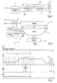
- the figure 1 represents, very schematically and in block form, the demodulation part in reception of radiofrequency signals by an electromagnetic transponder.
- the RF radio frequency signals After being received by an antenna and formatted by a coupler (not shown) the RF radio frequency signals are processed by an analog demodulator 1 (ANALOG DEMOD) whose role is to provide a demodulated analog AS signal and a CK clock sampling.
- the sampling clock is generally recovered from the transmission carrier.
- AS and CK signals are sent on an interface circuit 2 (INTERF) whose role is to provide an output signal O exploitable by a microcontroller 3 (CPU) and other digital circuits.
- the signal O is supplied to a data bus with which the central unit 3 communicates.
- a transmission from a terminal to a transponder is effected using a 13.56 MHz carrier on which coded information, generally in amplitude modulation with a non-zero modulation rate, is transmitted to a rate of 106 kilobits per second.
- the carrier is used to remotely power circuits of the transponder in the case where the latter is devoid of battery.
- the same principle of demodulation is used in a terminal with the difference that the clock signal is generally present therein without it being necessary to extract it from the received signal.
- the figure 2 illustrates, in chronograms, the principle of a demodulation carried out in a circuit as illustrated by the figure 1 .
- the first timing diagram illustrates an example of data D transmitted by the RF signal and to be recovered at the output O of the circuit 2.
- the transmission of a bit at the state 0 corresponds, within a bit time T, at a low level followed by a high level while the transmission of a 1 corresponds to the opposite (high level followed by a low level).
- the duration T corresponds, for example, to 106 kilohertz.
- an AS signal (second timing diagram) is obtained which roughly follows the trend of the signal D.
- the recovered clock signal CK (third timing) corresponds to the carrier signal, that is to say at a frequency of 13.56 Megahertz.
- the chronograms of the figure 2 are not to scale, especially in the time scale of the AS and CK timing diagrams.
- the last chronogram of the figure 2 represents the signal O.
- the signal AS is sampled once in the middle of a cycle (times t1 and t2). In fact, the signal AS is sent to the input of an inverter whose switching threshold TH conditions the output state O.
- a first disadvantage of a conventional demodulation system as illustrated by the Figures 1 and 2 is that, if the signal AS is highly disturbed, the instant t1 or t2, taking into account the signal level may provide a false result.
- the limit is in practice 106 kilobits per second to respect the time required for a software analysis of the data received.
- the present invention aims to optimize the demodulation of RF signals and in particular to increase the possible transmission rates for a given clock frequency.
- the invention also aims to propose a solution that eliminates possible problems of disturbance in the signal from an analog demodulator.
- the invention also aims to propose a solution that is compatible with conventional transponder architectures. electromagnetic and in particular with systems in which the clock is transmitted at the same time as the radiofrequency signal.
- said decision means receive an odd number of samples and provide the binary state of the symbol by applying a majority decision criterion.
- the respective positions of the significant samples are determined by a learning or characterization phase.
- the sampling signal is derived from the selected positions for the significant samples.
- the sampling signal corresponds to said frequency.
- the output of the analog-to-digital conversion element is sent to the input of a shift register whose parallel outputs are supplied to a multiplexer for selecting said significant samples.
- registers store at least the position in a symbol of a sample considered significant.
- the present invention is applied to a transmission system between an electromagnetic transponder and a read-write terminal.
- an odd number of samples is selected, the state of the symbol being determined by majority decision from the respective states of the different samples.
- the respective positions of the significant samples are determined by a learning phase.
- the sampling signal is derived from the selected positions for the significant samples.
- the sampling signal corresponds to said frequency.
- a feature of the present invention is to select, in one symbol, several samples and deduce from these samples the state 0 or 1 of the symbol without resorting to the central processing unit.
- the number of samples taken into account is less than the number of samples that would be obtained with sampling at the frequency on which the sampling signal is based.
- Another feature of the present invention is to select a reduced number of samples per symbol as corresponding to reliable samples at (temporal) positions decided during a learning or characterization phase, and to deduce the state of the symbol of these selected samples.
- the analog signal originating from an analog demodulator is directly sampled at times in the symbol corresponding to the instants providing the selected samples. This amounts to generating a sampling signal, based on a frequency of period less than the duration of a symbol, but whose number of fronts is less than that of this frequency.
- the sampling signal based on the sampling frequency is directly this frequency.
- the analog signal from the analog demodulator is then sampled at a frequency corresponding, preferably, to the maximum available frequency. We then deduce from several selected samples of the symbol state 0 or 1 of the latter.
- the figure 3 represents, very schematically and in block form, this second embodiment of a demodulator according to the invention.
- an RF radio frequency signal is received by an analog demodulator 2 (ANALOG DEMOD) responsible for extracting an analog signal AS as well as a clock signal CK at the frequency of the carrier, which here constitutes the sampling signal.
- ANALOG DEMOD analog demodulator 2
- the signal CK is transmitted to an interface circuit 2 which supplies the digital signals O to a central processing unit 3 (CPU) in the manner of the conventional circuit of the figure 1 .
- a demodulation optimization circuit 4 (DEMOPT) is interposed between the output of the analog demodulator 1 supplying the signal AS and the corresponding input of the interface circuit 2.
- This circuit 4 Furthermore, it receives the clock signal CK as well as control signals CT from the central unit 3.
- circuit 4 The role of circuit 4 is to provide a signal DS corresponding to the state 0 or 1 of the received symbol.
- the interface circuit 2 directly receives the states exploitable by the central unit 3.
- the circuit 2 may be omitted.
- the figure 4 represents an embodiment of a circuit 4 according to the present invention.
- the signal AS passes through an analog digital converter 10 (A / D) whose sampling frequency corresponds to the frequency of the clock signal CK.
- the output of the converter 10 is sent to a serial input of a shift register 11 (SREG) sized so that the length of a word it contains corresponds to the number of samples contained in a transmitted data symbol.
- SREG shift register 11
- All the bits of the register 11 are read in parallel and sent to inputs of a multiplexer 12 whose role is to select several samples as being significant to the state of the symbol.
- the multiplexer 12 selects an odd number of samples (for example, three) that it supplies to a decision circuit 13 (DECID) whose role is to determine the state of the symbol by applying a majority decision process .
- DECID decision circuit 13
- the output of circuit 13 provides the DS bit.
- the selection made by the multiplexer 12 is configurable.
- two registers 13 (NREG) and 14 (dREG) contain words respectively indicating the position N of a central sample in a range of samples considered reliable and the distance d between two samples of the significant range.
- the respective values of the registers 14 and 15 are then exploited by a calculation circuit 16 supplying the multiplexer 12 with the respective positions N of the central sample of the range and the respective positions N + d and Nd of the end samples.
- a calculation circuit 16 supplying the multiplexer 12 with the respective positions N of the central sample of the range and the respective positions N + d and Nd of the end samples.
- the symmetrical distance d can be replaced by differences that are different from each other between the positions of the samples.
- the respective contents of the registers 14 and 15 are loaded in the circuit 4 by the central unit 3 according to predetermined parameter data.
- the registers 14 and 15 respectively contain nibbles indicating the positions of the significant samples.
- the figure 5 illustrates, in the form of timing diagrams, the operation of an optimization circuit according to the invention. These chronograms represent, for states 1 and 0 transmitted respectively, the clock signal CK, the signal AS, the selection signals SEL of the multiplexer 12 and the output DS of the circuit 13.
- An advantage of the present invention is that it avoids any detection errors due to transient disturbances on the demodulated signals. Such a disturbance is illustrated in the right part of the figure 5 in the form of a peak p. It can clearly be seen that, in this case, despite the fact that the sample N is considered as a high state, the majority decision made by the circuit 13 makes it possible to confirm the state 0 of the bit transmitted.
- the most significant samples are determined during a characterization phase or product test or more precisely a batch of products.
- the invention thus takes advantage of the fact that the general appearance of the AS signal is most often repetitive for the same batch of integrated circuit chips.
- a learning phase is periodically carried out during the course of life of the product in order to adapt the demodulator to possible drifts.
- An advantage of the invention is that it makes it possible to accelerate the transmission rate for a given clock frequency, while remaining compatible with a software interpretation of the transmitted data. Indeed, the central unit does not intervene (outside the control phase of the registers 14 and 15) in the selection itself of the sample. It is therefore possible to increase the number of bits transmitted while respecting the possibility of interpretation by the central unit.
- the duration T 'of a symbol according to the invention can correspond to a rate of 847.5 kilobits per second.
- Such a factor 8 (compared to the conventional rate of 106 kbit / s) appears low but is in fact very advantageous. For example, an image that typically takes 4 seconds to be transmitted no longer, thanks to the invention a half-second. This speed becomes compatible with the needs of rapid analysis, especially in authentication or access control applications.
- demodulator thus constituted is parameterizable.
- the same hardware circuit can therefore be customized to be adapted to different integrated circuits.
Landscapes
- Engineering & Computer Science (AREA)
- Computer Networks & Wireless Communication (AREA)
- Signal Processing (AREA)
- Power Engineering (AREA)
- Digital Transmission Methods That Use Modulated Carrier Waves (AREA)
- Dc Digital Transmission (AREA)
Description
La présente invention concerne le domaine des démodulateurs et plus particulièrement les démodulateurs de signaux radiofréquence dont les résultats doivent être exploités par une unité de traitement numérique.The present invention relates to the field of demodulators and more particularly the radio frequency signal demodulators whose results must be exploited by a digital processing unit.
Le document
Un exemple d'application de la présente invention concerne les systèmes à transpondeurs électromagnétiques dans lesquels un transpondeur communique avec une borne de lecture-écriture sans contact.An exemplary application of the present invention relates to electromagnetic transponder systems in which a transponder communicates with a contactless read-write terminal.
La
Après avoir été reçus par une antenne et mis en forme par un coupleur (non représentés) les signaux radiofréquence RF sont traités par un démodulateur analogique 1 (ANALOG DEMOD) dont le rôle est de fournir un signal AS analogique démodulé ainsi qu'une horloge CK d'échantillonnage. L'horloge d'échantillonnage est récupérée généralement à partir de la porteuse de transmission. Les signaux AS et CK sont envoyés sur un circuit 2 d'interface (INTERF) dont le rôle est de fournir un signal de sortie O exploitable par un microcontrôleur 3 (CPU) et autres circuits numériques. En pratique, le signal O est fourni à un bus de données avec lequel communique l'unité centrale 3. Dans une application aux transpondeurs électromagnétiques, une transmission d'une borne vers un transpondeur s'effectue en utilisant une porteuse à 13,56 MHz sur laquelle sont transmises des informations codées, généralement en modulation d'amplitude avec un taux de modulation non nul, à un débit de 106 kilobits par seconde. Côté transpondeur, la porteuse sert à téléalimenter des circuits du transpondeur dans le cas où ce dernier est dépourvu de batterie. Le même principe de démodulation est utilisé dans une borne à la différence près que le signal d'horloge est généralement présent dans celle-ci sans qu'il soit nécessaire de l'extraire du signal reçu.After being received by an antenna and formatted by a coupler (not shown) the RF radio frequency signals are processed by an analog demodulator 1 (ANALOG DEMOD) whose role is to provide a demodulated analog AS signal and a CK clock sampling. The sampling clock is generally recovered from the transmission carrier. AS and CK signals are sent on an interface circuit 2 (INTERF) whose role is to provide an output signal O exploitable by a microcontroller 3 (CPU) and other digital circuits. In practice, the signal O is supplied to a data bus with which the
La
Le premier chronogramme illustre un exemple de données D transmis par le signal RF et devant être récupéré en sortie O du circuit 2. Dans cet exemple, on suppose que la transmission d'un bit à l'état 0 correspond, à l'intérieur d'un temps de bit T, à un niveau bas suivi d'un niveau haut tandis que la transmission d'un 1 correspond à l'inverse (niveau haut suivi d'un niveau bas). Il s'agit là d'un exemple et différents types de codages et de transmission sont susceptibles d'être utilisés. Dans l'exemple des transpondeurs électromagnétiques utilisant une fréquence de porteuse à 13,56 Mégahertz, la durée T correspond, par exemple, à 106 kilohertz.The first timing diagram illustrates an example of data D transmitted by the RF signal and to be recovered at the output O of the circuit 2. In this example, it is assumed that the transmission of a bit at the
En sortie du démodulateur analogique 1, on obtient un signal AS (deuxième chronogramme) qui suit grossièrement l'allure du signal D.At the output of the
Le signal CK d'horloge récupéré (troisième chronogramme) correspond au signal de la porteuse, c'est-à-dire à une fréquence de 13,56 Mégahertz. Pour des raisons de clarté, les chronogrammes de la
Le dernier chronogramme de la
Dans un circuit 2 classique, le signal AS est échantillonné une seule fois au milieu d'un cycle (instants t1 et t2) . En fait, le signal AS est envoyé en entrée d'un inverseur dont le seuil de basculement TH conditionne l'état fourni en sortie O.In a conventional circuit 2, the signal AS is sampled once in the middle of a cycle (times t1 and t2). In fact, the signal AS is sent to the input of an inverter whose switching threshold TH conditions the output state O.
Un premier inconvénient d'un système de démodulation classique tel qu'illustré par les
Un autre inconvénient est qu'il n'est pas possible de rapprocher les différents instants d'analyse du signal AS dans la mesure où cela conduirait à des vitesses incompatibles avec la vitesse de travail de l'unité centrale dont la fréquence d'horloge correspond au maximum à la fréquence de l'horloge CK. Par conséquent, le débit est limité.Another disadvantage is that it is not possible to approximate the different analysis instants of the AS signal insofar as this would lead to speeds incompatible with the working speed of the central unit whose clock frequency corresponds at the maximum frequency of the clock CK. Therefore, the flow is limited.
En reprenant l'exemple des systèmes à transpondeurs électromagnétiques basés sur une fréquence de 13,56 Mégahertz, la limite est en pratique de 106 kilobits par seconde pour respecter le temps nécessaire à une analyse logicielle des données reçues.Using the example of 13.56 Megahertz frequency electromagnetic transponder systems, the limit is in practice 106 kilobits per second to respect the time required for a software analysis of the data received.
Il serait souhaitable de pouvoir accroître la vitesse de transmission de tels systèmes. Par exemple, dans une application où l'on souhaite transmettre des images (photographiques, empreintes biométriques), un débit de 106 kilobits par seconde entraîne des temps de transmission de plusieurs secondes, incompatible avec les vitesses d'analyse souhaitées.It would be desirable to be able to increase the transmission speed of such systems. For example, in an application where it is desired to transmit images (photographic, biometric fingerprints), a rate of 106 kilobits per second results in transmission times of several seconds, incompatible with the desired analysis speeds.
La présente invention vise à optimiser la démodulation de signaux RF et en particulier à accroître les débits de transmission possibles pour une fréquence d'horloge donnée.The present invention aims to optimize the demodulation of RF signals and in particular to increase the possible transmission rates for a given clock frequency.
L'invention vise également à proposer une solution qui s'affranchisse des problèmes éventuels de perturbation dans le signal issu d'un démodulateur analogique.The invention also aims to propose a solution that eliminates possible problems of disturbance in the signal from an analog demodulator.
L'invention vise également à proposer une solution qui soit compatible avec les architectures classiques de transpondeurs électromagnétiques et notamment avec des systèmes dans lesquels l'horloge est transmise en même temps que le signal radiofréquence.The invention also aims to propose a solution that is compatible with conventional transponder architectures. electromagnetic and in particular with systems in which the clock is transmitted at the same time as the radiofrequency signal.
Pour atteindre ces objets ainsi que d'autres, la présente invention prévoit un circuit de détection d'un état binaire porté par un symbole analogique, comportant :
- un élément de conversion analogique-numérique utilisant un signal d'échantillonnage basé sur une fréquence de période inférieure à la durée d'un symbole ;
- des moyens de sélection d'un nombre d'échantillons significatifs inférieur au nombre d'échantillons qui serait obtenu avec un échantillonnage du symbole à ladite fréquence ; et
- des moyens de décision de l'état du symbole à partir des échantillons sélectionnés.
- an analog-to-digital conversion element using a sampling signal based on a period frequency less than the duration of a symbol;
- means for selecting a number of significant samples smaller than the number of samples that would be obtained with a sampling of the symbol at said frequency; and
- decision means of the state of the symbol from the selected samples.
Selon un mode de réalisation de la présente invention, lesdits moyens de décision reçoivent un nombre impair d'échantillons et fournissent l'état binaire du symbole en appliquant un critère de décision majoritaire.According to an embodiment of the present invention, said decision means receive an odd number of samples and provide the binary state of the symbol by applying a majority decision criterion.
Selon un mode de réalisation de la présente invention, les positions respectives des échantillons significatifs sont déterminées par une phase d'apprentissage ou de caractérisation.According to one embodiment of the present invention, the respective positions of the significant samples are determined by a learning or characterization phase.
Selon un mode de réalisation de la présente invention, le signal d'échantillonnage est dérivé des positions choisies pour les échantillons significatifs.According to one embodiment of the present invention, the sampling signal is derived from the selected positions for the significant samples.
Selon un mode de réalisation de la présente invention, le signal d'échantillonnage correspond à ladite fréquence.According to an embodiment of the present invention, the sampling signal corresponds to said frequency.
Selon un mode de réalisation de la présente invention, la sortie de l'élément de conversion analogique-numérique est envoyée en entrée d'un registre à décalage dont les sorties parallèles sont fournies à un multiplexeur de sélection desdits échantillons significatifs.According to an embodiment of the present invention, the output of the analog-to-digital conversion element is sent to the input of a shift register whose parallel outputs are supplied to a multiplexer for selecting said significant samples.
Selon un mode de réalisation de la présente invention, des registres stockent au moins la position dans un symbole d'un échantillon considéré comme significatif.According to one embodiment of the present invention, registers store at least the position in a symbol of a sample considered significant.
Selon un mode de réalisation de la présente invention, elle est appliquée à un système de transmission entre un transpondeur électromagnétique et une borne de lecture-écriture.According to one embodiment of the present invention, it is applied to a transmission system between an electromagnetic transponder and a read-write terminal.
L'invention prévoit également un procédé de détermination d'un état binaire porté par un symbole analogique, consistant à :
- échantillonner le symbole avec un signal d'échantillonnage basé sur une fréquence de période inférieure à la durée d'un symbole ;
- sélectionner un nombre d'échantillons significatifs inférieur au nombre d'échantillons qui serait obtenu avec un échantillonnage du symbole à ladite fréquence ; et
- décider de l'état du symbole à partir des échantillons sélectionnés.
- sampling the symbol with a sampling signal based on a period frequency less than the duration of a symbol;
- select a number of significant samples smaller than the number of samples that would be obtained with a sampling of the symbol at said frequency; and
- decide the state of the symbol from the selected samples.
Selon un mode de mise en oeuvre de la présente invention, un nombre impair d'échantillons est sélectionné, l'état du symbole étant déterminé par décision majoritaire à partir des états respectifs des différents échantillons.According to an embodiment of the present invention, an odd number of samples is selected, the state of the symbol being determined by majority decision from the respective states of the different samples.
Selon un mode de réalisation de la présente invention, les positions respectives des échantillons significatifs sont déterminées par une phase d'apprentissage.According to one embodiment of the present invention, the respective positions of the significant samples are determined by a learning phase.
Selon un mode de réalisation de la présente invention, le signal d'échantillonnage est dérivé des positions choisies pour les échantillons significatifs.According to one embodiment of the present invention, the sampling signal is derived from the selected positions for the significant samples.
Selon un mode de réalisation de la présente invention, le signal d'échantillonnage correspond à ladite fréquence.According to an embodiment of the present invention, the sampling signal corresponds to said frequency.
Ces objets, caractéristiques et avantages, ainsi que d'autres de la présente invention seront exposés en détail dans la description suivante de modes de réalisation particuliers faite à titre non-limitatif en relation avec les figures jointes parmi lesquelles :
- la
figure 1 décrite précédemment représente une architecture de démodulation classique ; - la
figure 2 décrite précédemment illustre le fonctionnement du démodulateur de lafigure 1 ; - la
figure 3 représente, de façon très schématique et sous forme de blocs, un exemple d'architecture d'un démodulateur selon l'invention ; - la
figure 4 représente un mode de réalisation d'un optimiseur de démodulation selon l'invention ; et - la
figure 5 illustre, sous forme de chronogramme, le fonctionnement d'un optimiseur de démodulation selon l'invention.
- the
figure 1 described above represents a classical demodulation architecture; - the
figure 2 described above illustrates the operation of the demodulator of thefigure 1 ; - the
figure 3 represents, very schematically and in block form, an exemplary architecture of a demodulator according to the invention; - the
figure 4 represents an embodiment of a demodulation optimizer according to the invention; and - the
figure 5 illustrates, in the form of a timing diagram, the operation of a demodulation optimizer according to the invention.
Les mêmes éléments ont été désignés par les mêmes références aux différentes figures. Pour des raisons de clarté, seuls les éléments qui sont nécessaires à la compréhension de l'invention ont été représentés aux figures et seront décrits par la suite. En particulier, les circuits avals au démodulateur n'ont pas été détaillés, l'invention étant compatible avec toute exploitation logicielle classique des signaux. De même, la structure interne d'un démodulateur analogique utilisé pour l'invention correspond à une structure classique et n'a pas été détaillée.The same elements have been designated by the same references in the different figures. For the sake of clarity, only the elements that are necessary for understanding the invention have been shown in the figures and will be described later. In particular, the downstream circuits to the demodulator have not been detailed, the invention being compatible with any conventional software operation of the signals. Similarly, the internal structure of an analog demodulator used for the invention corresponds to a conventional structure and has not been detailed.
Une caractéristique de la présente invention est de sélectionner, dans un symbole, plusieurs échantillons et de déduire de ces échantillons l'état 0 ou 1 du symbole sans recourir à l'unité centrale de traitement. Selon l'invention, le nombre d'échantillons pris en compte est inférieur au nombre d'échantillons qui serait obtenu avec un échantillonnage à la fréquence sur laquelle est basé le signal d'échantillonnage.A feature of the present invention is to select, in one symbol, several samples and deduce from these samples the
Une autre caractéristique de la présente invention est de sélectionner un nombre réduit d'échantillons par symbole comme correspondant à des échantillons fiables en des positions (temporelles) décidées lors d'une phase d'apprentissage ou de caractérisation, et de déduire l'état du symbole de ces échantillons sélectionnés.Another feature of the present invention is to select a reduced number of samples per symbol as corresponding to reliable samples at (temporal) positions decided during a learning or characterization phase, and to deduce the state of the symbol of these selected samples.
Selon un premier mode de réalisation non représenté, on échantillonne directement le signal analogique issu d'un démodulateur analogique à des instants dans le symbole qui correspondent aux instants fournissant les échantillons sélectionnés. Cela revient à générer un signal d'échantillonnage, basé sur une fréquence de période inférieure à la durée d'un symbole, mais dont le nombre de fronts est inférieur à celui de cette fréquence.According to a first embodiment not shown, the analog signal originating from an analog demodulator is directly sampled at times in the symbol corresponding to the instants providing the selected samples. This amounts to generating a sampling signal, based on a frequency of period less than the duration of a symbol, but whose number of fronts is less than that of this frequency.
Selon un deuxième mode de réalisation, le signal d'échantillonnage basé sur la fréquence d'échantillonnage est directement cette fréquence. Le signal analogique issu du démodulateur analogique est alors échantillonné à une fréquence correspondant, de préférence, à la fréquence maximale disponible. On déduit ensuite de plusieurs échantillons sélectionnés du symbole l'état 0 ou 1 de ce dernier.According to a second embodiment, the sampling signal based on the sampling frequency is directly this frequency. The analog signal from the analog demodulator is then sampled at a frequency corresponding, preferably, to the maximum available frequency. We then deduce from several selected samples of the
La
Comme précédemment, un signal radio fréquence RF est reçu par un démodulateur analogique 2 (ANALOG DEMOD) chargé d'extraire un signal analogique AS ainsi qu'un signal d'horloge CK à la fréquence de la porteuse qui constitue ici le signal d'échantillonnage. Le signal CK est transmis à un circuit 2 d'interface qui fournit les signaux numériques O à une unité centrale de traitement 3 (CPU) à la manière du circuit classique de la
Selon ce mode de réalisation de l'invention, un circuit d'optimisation de la démodulation 4 (DEMOPT) est intercalé entre la sortie du démodulateur analogique 1 fournissant le signal AS et l'entrée correspondante du circuit d'interface 2. Ce circuit 4 reçoit par ailleurs le signal d'horloge CK ainsi que des signaux de commande CT de l'unité centrale 3.According to this embodiment of the invention, a demodulation optimization circuit 4 (DEMOPT) is interposed between the output of the
Le circuit 4 a pour rôle de fournir un signal DS correspondant à l'état 0 ou 1 du symbole reçu. Ainsi, le circuit d'interface 2 reçoit directement les états exploitables par l'unité centrale 3. Selon une variante de réalisation et sous réserve de la compatibilité électrique des signaux O avec le bus de liaison avec l'unité centrale 3, le circuit 2 peut le cas échéant être omis.The role of
La
Le signal AS traverse un convertisseur analogique numérique 10 (A/D) dont la fréquence d'échantillonnage correspond à la fréquence du signal d'horloge CK. La sortie du convertisseur 10 est envoyée sur une entrée série d'un registre à décalage 11 (SREG) dimensionné pour que la longueur d'un mot qu'il contient corresponde au nombre d'échantillons contenu dans un symbole de données transmis.The signal AS passes through an analog digital converter 10 (A / D) whose sampling frequency corresponds to the frequency of the clock signal CK. The output of the
Tous les bits du registre 11 sont lus en parallèle et envoyés sur des entrées d'un multiplexeur 12 dont le rôle est de sélectionner plusieurs échantillons comme étant significatifs de l'état du symbole.All the bits of the
De préférence et comme illustré par la
Selon un mode de réalisation préféré, la sélection opérée par le multiplexeur 12 est paramétrable. Par exemple, deux registres 13 (NREG) et 14 (dREG) contiennent des mots indicateurs respectivement de la position N d'un échantillon central dans une plage d'échantillons considérés comme fiables et la distance d entre deux d'échantillons de la plage significative. Les valeurs respectives des registres 14 et 15 sont alors exploitées par un circuit de calcul 16 fournissant au multiplexeur 12 les positions respectives N de l'échantillon central de la plage et les positions respectives N+d et N-d des échantillons d'extrémité. Il s'agit là d'un exemple de génération de signaux de sélection SEL mais tout autre moyen pourra être utilisé. Par exemple, la distance d symétrique peut être remplacée par des écarts différents les uns des autres entre les positions des échantillons.According to a preferred embodiment, the selection made by the
Les contenus respectifs des registres 14 et 15 sont chargés dans le circuit 4 par unité centrale 3 en fonction de données de paramétrage prédéterminées. Dans un exemple particulier où la taille du registre 11 est de 16 bits, les registres 14 et 15 contiennent respectivement des quartets indiquant les positions des échantillons significatifs.The respective contents of the
La
On suppose un signal AS ayant une forme perturbée de façon classique. Ce signal est échantillonné à la fréquence de l'horloge CK et le multiplexeur sélectionne trois échantillons désignés par leur position respective N-d et N+d. Dans l'exemple de la
Un avantage de la présente invention est qu'elle évite les éventuelles erreurs de détection dues à des perturbations transitoires sur les signaux démodulés. Une telle perturbation est illustrée en partie droite de la
Selon un premier mode de mise en oeuvre de l'invention, les échantillons les plus significatifs sont déterminés pendant une phase de caractérisation ou de test du produit ou plus précisément d'un lot de produits. L'invention tire alors profit du fait que l'allure générale du signal AS est le plus souvent répétitive pour un même lot de puces de circuit intégré.According to a first embodiment of the invention, the most significant samples are determined during a characterization phase or product test or more precisely a batch of products. The invention thus takes advantage of the fact that the general appearance of the AS signal is most often repetitive for the same batch of integrated circuit chips.
Selon un deuxième mode de mise en oeuvre, une phase d'apprentissage est effectuée périodiquement au cours de la vie du produit afin d'adapter le démodulateur à d'éventuelles dérives. Ces deux modes de mise en oeuvre sont combinables.According to a second mode of implementation, a learning phase is periodically carried out during the course of life of the product in order to adapt the demodulator to possible drifts. These two modes of implementation are combinable.
La mise en oeuvre d'une phase d'apprentissage ou de caractérisation n'entraîne pas de difficulté particulière. Il suffit de connaître la nature du message transmis, de faire plusieurs paramétrages différents des registres 14 et 15 et de sélectionner le premier paramétrage qui donne un résultat correct sur un nombre (considéré comme significatif) de symboles.The implementation of a learning phase or characterization does not cause any particular difficulty. It suffices to know the nature of the message transmitted, to make several different settings of the
Un avantage de l'invention est qu'elle permet d'accélérer le débit de transmission pour une fréquence d'horloge donnée, tout en restant compatible avec une interprétation logicielle des données transmises. En effet, l'unité centrale n'intervient pas (hors de la phase de commande des registres 14 et 15) dans la sélection elle-même de l'échantillon. Il est donc possible d'accroître le nombre de bits transmis tout en respectant la possibilité d'interprétation par l'unité centrale.An advantage of the invention is that it makes it possible to accelerate the transmission rate for a given clock frequency, while remaining compatible with a software interpretation of the transmitted data. Indeed, the central unit does not intervene (outside the control phase of the
Ainsi, en reprenant l'exemple des transpondeurs électromagnétiques, sur une porteuse de 13,56 Mégahertz, la durée T' d'un symbole selon l'invention peut correspondre à un débit de 847,5 kilobits par seconde. Un tel facteur 8 (par rapport au débit classique de 106 kbits/s) paraît faible mais est en fait très avantageux. Par exemple, une image qui met classiquement 4 secondes à être transmise ne met plus, grâce à l'invention qu'une demi-seconde. Cette vitesse devient compatible avec les besoins d'analyse rapide, notamment dans des applications d'authentification ou de contrôle d'accès.Thus, using the example of electromagnetic transponders, on a carrier of 13.56 Megahertz, the duration T 'of a symbol according to the invention can correspond to a rate of 847.5 kilobits per second. Such a factor 8 (compared to the conventional rate of 106 kbit / s) appears low but is in fact very advantageous. For example, an image that typically takes 4 seconds to be transmitted no longer, thanks to the invention a half-second. This speed becomes compatible with the needs of rapid analysis, especially in authentication or access control applications.
Un autre avantage de la présente invention est que le démodulateur ainsi constitué est paramétrable. Un même circuit matériel peut donc être personnalisé pour être adapté à des circuits intégrés différents.Another advantage of the present invention is that the demodulator thus constituted is parameterizable. The same hardware circuit can therefore be customized to be adapted to different integrated circuits.
Bien entendu, la présente invention est susceptible de diverses variantes et modifications qui apparaîtront à l'homme de l'art. En particulier, d'autres fréquences et débits que ceux indiqués ci-dessus pourront être exploités.Of course, the present invention is susceptible of various variations and modifications which will be apparent to those skilled in the art. In particular, other frequencies and speeds than those indicated above may be exploited.
De plus, bien que l'invention ait été décrite plus particulièrement en relation avec une accélération du débit, elle permet, même à débit constant, d'améliorer la fiabilité d'un démodulateur analogique.In addition, although the invention has been described more particularly in relation to an acceleration of the flow, it makes it possible, even at a constant flow rate, to improve the reliability of an analog demodulator.
En outre, la mise en oeuvre pratique de l'invention est à la portée de l'homme du métier, que ce soit par des moyens matériels et/ou logiciels à partir de la description fonctionnelle donnée ci-dessus.In addition, the practical implementation of the invention is within the abilities of those skilled in the art, whether by hardware and / or software from the functional description given above.
Enfin, l'adaptation de l'exemple représenté au premier mode de réalisation dans lequel la sélection est directement opérée sur les instants d'échantillonnage plutôt que sur les échantillons eux-mêmes est également à la portée de l'homme du métier en utilisant des composants en eux-mêmes connus.Finally, the adaptation of the example shown in the first embodiment in which the selection is made directly on the sampling instants rather than on the samples themselves is also within the abilities of those skilled in the art using components in themselves known.
Claims (13)
- A circuit (4) for detecting a binary state supported by an analog symbol (AS), characterized in that it comprises:an analog-to-digital conversion element (10) using a sampling signal based on a frequency (CK) having a period shorter than the duration of a symbol;means (11, 12, 14, 15, 16) for selecting a number of significant samples smaller than the number of samples which would be obtained with a sampling of the symbol at said frequency; andmeans (13) for deciding the symbol state based on the selected samples.
- The circuit of claim 1, wherein said decision means (13) receive an odd number of samples and provide the binary state of the symbol by applying a majority decision criterion.
- The circuit of claim 1 or 2, wherein the respective positions (N, N-d, N+d) of the significant samples are determined in a training or characterization phase.
- The circuit of claim 3, wherein the sampling signal is derived from the positions selected for the significant samples.
- The circuit of any of claims 1 to 3, wherein the sampling signal corresponds to said frequency.
- The circuit of claim 5, wherein the output of the analog-to-digital conversion element (10) is sent to the input of a shift register (11) having its parallel outputs provided to a multiplexer (12) for selecting said significant samples.
- The circuit of any of claims 1 to 6, wherein registers (14, 15) store at least the position (N) in a symbol of a sample considered as being significant.
- The circuit of any of claims 1 to 7, applied to a system of transmission between an electromagnetic transponder and a read/write terminal.
- A method for determining a binary state supported by an analog symbol (AS), characterized in that it consists of:sampling (10) the symbol with a sampling signal based on a frequency (CK) having a period shorter than the duration of a symbol;selecting (11, 12, 14, 15, 16) a number of significant samples smaller than the number of samples which would be obtained with a sampling of the symbol at said frequency; anddeciding (13) the symbol state based on the selected samples.
- The method of claim 9, wherein an odd number of samples is selected, the symbol state being determined by majority decision based on the respective states of the different samples.
- The method of claim 9 or 10, wherein the respective positions of the significant samples are determined by a training phase.
- The method of claim 11, wherein the sampling signal is derived from the positions selected for the significant samples.
- The method of any of claims 9 to 11, wherein the sampling signal (CK) corresponds to said frequency.
Applications Claiming Priority (2)
| Application Number | Priority Date | Filing Date | Title |
|---|---|---|---|
| FR0450746 | 2004-04-21 | ||
| FR0450746 | 2004-04-21 |
Publications (2)
| Publication Number | Publication Date |
|---|---|
| EP1592136A1 EP1592136A1 (en) | 2005-11-02 |
| EP1592136B1 true EP1592136B1 (en) | 2012-07-11 |
Family
ID=34939390
Family Applications (1)
| Application Number | Title | Priority Date | Filing Date |
|---|---|---|---|
| EP05103149A Expired - Lifetime EP1592136B1 (en) | 2004-04-21 | 2005-04-19 | Adaptive demodulator |
Country Status (3)
| Country | Link |
|---|---|
| US (1) | US8243856B2 (en) |
| EP (1) | EP1592136B1 (en) |
| JP (1) | JP5242000B2 (en) |
Families Citing this family (2)
| Publication number | Priority date | Publication date | Assignee | Title |
|---|---|---|---|---|
| JP6497988B2 (en) * | 2015-03-12 | 2019-04-10 | 東京瓦斯株式会社 | Portable terminal device, gas meter output analysis system using portable terminal device, and gas meter output analysis method |
| CN114745021B (en) * | 2022-02-18 | 2024-01-23 | 中国人民解放军陆军工程大学 | Non-homologous code rate tracking method for deep space transponder |
Family Cites Families (12)
| Publication number | Priority date | Publication date | Assignee | Title |
|---|---|---|---|---|
| CA1068822A (en) * | 1974-06-24 | 1979-12-25 | Ching-Long Song | Digital to analog converter for a communication system |
| DE3009785A1 (en) * | 1980-03-14 | 1981-10-01 | Deutsche Itt Industries Gmbh, 7800 Freiburg | SPECTRAL ANALYZER |
| US4745625A (en) * | 1986-03-12 | 1988-05-17 | Codex Corporation | Transition detector |
| US5052000A (en) * | 1989-06-09 | 1991-09-24 | At&T Bell Laboratories | Technique for improving the operation of decision feedback equalizers in communications systems utilizing error correction |
| US5751884A (en) * | 1989-12-30 | 1998-05-12 | Samsung Electronics Co., Ltd. | High-resolution video tape recorder systems and methods for recording and recovering video compatibly with the normal-VHS format system |
| US6229856B1 (en) * | 1997-04-14 | 2001-05-08 | Masimo Corporation | Method and apparatus for demodulating signals in a pulse oximetry system |
| US6850563B1 (en) * | 1998-06-19 | 2005-02-01 | Netwave Communications | Data slicer for combined trellis decoding and equalization |
| JP2000031951A (en) | 1998-07-15 | 2000-01-28 | Fujitsu Ltd | Burst synchronization circuit |
| US6100835A (en) * | 1998-09-10 | 2000-08-08 | Spacecode Llc | Multi-symbol analysis for digital symbol determination |
| JP2001053734A (en) * | 1999-08-06 | 2001-02-23 | Matsushita Electric Ind Co Ltd | Optical receiver circuit for burst optical signal |
| DE60022464T2 (en) * | 2000-01-11 | 2006-06-14 | Lucent Technologies Inc | Correction of frequency offset in intersymbol interference |
| US7359458B2 (en) * | 2003-07-31 | 2008-04-15 | Analog Devices, Inc. | Structures and methods for capturing data from data bit streams |
-
2005
- 2005-04-19 EP EP05103149A patent/EP1592136B1/en not_active Expired - Lifetime
- 2005-04-20 JP JP2005122185A patent/JP5242000B2/en not_active Expired - Lifetime
- 2005-04-21 US US11/111,241 patent/US8243856B2/en active Active
Also Published As
| Publication number | Publication date |
|---|---|
| US20050238120A1 (en) | 2005-10-27 |
| US8243856B2 (en) | 2012-08-14 |
| JP2005312051A (en) | 2005-11-04 |
| JP5242000B2 (en) | 2013-07-17 |
| EP1592136A1 (en) | 2005-11-02 |
Similar Documents
| Publication | Publication Date | Title |
|---|---|---|
| WO2022073968A1 (en) | Electronic payment terminal and method for detecting a corresponding payment mode | |
| FR2635207A1 (en) | Method and device for processing an analog electrical signal with a view to obtaining a binary signal whose parameters can be analysed which is representative of its significant component | |
| EP0451232B1 (en) | Code acquisition method and circuit for a spread spectrum signal receiver | |
| FR2754366A1 (en) | FILTER COPROCESSOR | |
| FR3036566B1 (en) | METHOD FOR SELECTING A FILTER FOR APPLICATION IN RECEPTION OF A FRAME | |
| EP1592136B1 (en) | Adaptive demodulator | |
| WO2002052521A2 (en) | Radiofrequency receiver for remote meter reading and remote meter reading method comprising same | |
| EP0224315B1 (en) | Digital frequency discriminator and its use in a composite vor signal | |
| EP1094631A1 (en) | Quest for the optimum sampling point in a TDMA packet transmission system | |
| EP0094040A2 (en) | System for synchronous data transmission with the aid of a constant envelope amplitude-modulated carrier | |
| EP1705604A1 (en) | Multilevel demodulation method and device | |
| EP1649663B1 (en) | Transmission protocol automatic detection method for a portable object such as a chip card or a chip key | |
| EP2106031B1 (en) | Method of identifying data coded by PPM modulation, receiver for this method | |
| EP3116181B1 (en) | Rfid receiver with very high throughput | |
| EP1131772B1 (en) | Digital transmission method | |
| EP0905946B1 (en) | Control of the sampling of biphase signals | |
| WO2002035466A1 (en) | Circuit for detecting and formatting data frames | |
| EP0113269B1 (en) | Method for discriminating noise and movement in a video image sequence and movement detecting device for carrying out the method | |
| EP0343083B1 (en) | Loss of synchronisation detection device, and its use in a digital transmission network | |
| EP1580893B1 (en) | Device and method for phase detection of a signal | |
| FR2877800A1 (en) | Digital signal decoder for direct sequence spread spectrum transmission system, has analysis circuit identifying filters adapted to input signal and controlling clock circuits to produce clock signals | |
| EP1835296B1 (en) | Method of characterising a bit detection instant | |
| FR2633138A1 (en) | METHOD AND DEVICE FOR EVALUATING THE SECURITY MARGIN OF A DIGITAL VIDEO SIGNAL | |
| EP1720308B1 (en) | Digital receiver | |
| EP0013857A1 (en) | Demodulation device for a frequency shift modulated analog signal |
Legal Events
| Date | Code | Title | Description |
|---|---|---|---|
| PUAI | Public reference made under article 153(3) epc to a published international application that has entered the european phase |
Free format text: ORIGINAL CODE: 0009012 |
|
| AK | Designated contracting states |
Kind code of ref document: A1 Designated state(s): AT BE BG CH CY CZ DE DK EE ES FI FR GB GR HU IE IS IT LI LT LU MC NL PL PT RO SE SI SK TR |
|
| AX | Request for extension of the european patent |
Extension state: AL BA HR LV MK YU |
|
| 17P | Request for examination filed |
Effective date: 20060421 |
|
| AKX | Designation fees paid |
Designated state(s): DE FR GB IT |
|
| 17Q | First examination report despatched |
Effective date: 20100628 |
|
| GRAP | Despatch of communication of intention to grant a patent |
Free format text: ORIGINAL CODE: EPIDOSNIGR1 |
|
| GRAS | Grant fee paid |
Free format text: ORIGINAL CODE: EPIDOSNIGR3 |
|
| GRAA | (expected) grant |
Free format text: ORIGINAL CODE: 0009210 |
|
| AK | Designated contracting states |
Kind code of ref document: B1 Designated state(s): DE FR GB IT |
|
| REG | Reference to a national code |
Ref country code: GB Ref legal event code: FG4D Free format text: NOT ENGLISH |
|
| REG | Reference to a national code |
Ref country code: DE Ref legal event code: R096 Ref document number: 602005035086 Country of ref document: DE Effective date: 20120906 |
|
| PLBE | No opposition filed within time limit |
Free format text: ORIGINAL CODE: 0009261 |
|
| STAA | Information on the status of an ep patent application or granted ep patent |
Free format text: STATUS: NO OPPOSITION FILED WITHIN TIME LIMIT |
|
| PG25 | Lapsed in a contracting state [announced via postgrant information from national office to epo] |
Ref country code: IT Free format text: LAPSE BECAUSE OF FAILURE TO SUBMIT A TRANSLATION OF THE DESCRIPTION OR TO PAY THE FEE WITHIN THE PRESCRIBED TIME-LIMIT Effective date: 20120711 |
|
| 26N | No opposition filed |
Effective date: 20130412 |
|
| REG | Reference to a national code |
Ref country code: DE Ref legal event code: R097 Ref document number: 602005035086 Country of ref document: DE Effective date: 20130412 |
|
| PGFP | Annual fee paid to national office [announced via postgrant information from national office to epo] |
Ref country code: FR Payment date: 20130603 Year of fee payment: 9 |
|
| GBPC | Gb: european patent ceased through non-payment of renewal fee |
Effective date: 20130419 |
|
| PG25 | Lapsed in a contracting state [announced via postgrant information from national office to epo] |
Ref country code: GB Free format text: LAPSE BECAUSE OF NON-PAYMENT OF DUE FEES Effective date: 20130419 |
|
| PGFP | Annual fee paid to national office [announced via postgrant information from national office to epo] |
Ref country code: DE Payment date: 20140321 Year of fee payment: 10 |
|
| REG | Reference to a national code |
Ref country code: FR Ref legal event code: ST Effective date: 20141231 |
|
| PG25 | Lapsed in a contracting state [announced via postgrant information from national office to epo] |
Ref country code: FR Free format text: LAPSE BECAUSE OF NON-PAYMENT OF DUE FEES Effective date: 20140430 |
|
| REG | Reference to a national code |
Ref country code: DE Ref legal event code: R119 Ref document number: 602005035086 Country of ref document: DE |
|
| PG25 | Lapsed in a contracting state [announced via postgrant information from national office to epo] |
Ref country code: DE Free format text: LAPSE BECAUSE OF NON-PAYMENT OF DUE FEES Effective date: 20151103 |