EP1591946A2 - RF tag reader/writer and printer containing the RF tag reader/writer - Google Patents
RF tag reader/writer and printer containing the RF tag reader/writer Download PDFInfo
- Publication number
- EP1591946A2 EP1591946A2 EP05008990A EP05008990A EP1591946A2 EP 1591946 A2 EP1591946 A2 EP 1591946A2 EP 05008990 A EP05008990 A EP 05008990A EP 05008990 A EP05008990 A EP 05008990A EP 1591946 A2 EP1591946 A2 EP 1591946A2
- Authority
- EP
- European Patent Office
- Prior art keywords
- tag
- antenna
- writer
- tag reader
- paper
- Prior art date
- Legal status (The legal status is an assumption and is not a legal conclusion. Google has not performed a legal analysis and makes no representation as to the accuracy of the status listed.)
- Granted
Links
Images




Classifications
-
- G—PHYSICS
- G06—COMPUTING OR CALCULATING; COUNTING
- G06K—GRAPHICAL DATA READING; PRESENTATION OF DATA; RECORD CARRIERS; HANDLING RECORD CARRIERS
- G06K17/00—Methods or arrangements for effecting co-operative working between equipments covered by two or more of main groups G06K1/00 - G06K15/00, e.g. automatic card files incorporating conveying and reading operations
- G06K17/0022—Methods or arrangements for effecting co-operative working between equipments covered by two or more of main groups G06K1/00 - G06K15/00, e.g. automatic card files incorporating conveying and reading operations arrangements or provisions for transferring data to distant stations, e.g. from a sensing device
-
- G—PHYSICS
- G06—COMPUTING OR CALCULATING; COUNTING
- G06K—GRAPHICAL DATA READING; PRESENTATION OF DATA; RECORD CARRIERS; HANDLING RECORD CARRIERS
- G06K17/00—Methods or arrangements for effecting co-operative working between equipments covered by two or more of main groups G06K1/00 - G06K15/00, e.g. automatic card files incorporating conveying and reading operations
- G06K17/0022—Methods or arrangements for effecting co-operative working between equipments covered by two or more of main groups G06K1/00 - G06K15/00, e.g. automatic card files incorporating conveying and reading operations arrangements or provisions for transferring data to distant stations, e.g. from a sensing device
- G06K17/0025—Methods or arrangements for effecting co-operative working between equipments covered by two or more of main groups G06K1/00 - G06K15/00, e.g. automatic card files incorporating conveying and reading operations arrangements or provisions for transferring data to distant stations, e.g. from a sensing device the arrangement consisting of a wireless interrogation device in combination with a device for optically marking the record carrier
-
- G—PHYSICS
- G06—COMPUTING OR CALCULATING; COUNTING
- G06K—GRAPHICAL DATA READING; PRESENTATION OF DATA; RECORD CARRIERS; HANDLING RECORD CARRIERS
- G06K7/00—Methods or arrangements for sensing record carriers, e.g. for reading patterns
- G06K7/10—Methods or arrangements for sensing record carriers, e.g. for reading patterns by electromagnetic radiation, e.g. optical sensing; by corpuscular radiation
- G06K7/10009—Methods or arrangements for sensing record carriers, e.g. for reading patterns by electromagnetic radiation, e.g. optical sensing; by corpuscular radiation sensing by radiation using wavelengths larger than 0.1 mm, e.g. radio-waves or microwaves
- G06K7/10316—Methods or arrangements for sensing record carriers, e.g. for reading patterns by electromagnetic radiation, e.g. optical sensing; by corpuscular radiation sensing by radiation using wavelengths larger than 0.1 mm, e.g. radio-waves or microwaves using at least one antenna particularly designed for interrogating the wireless record carriers
-
- G—PHYSICS
- G06—COMPUTING OR CALCULATING; COUNTING
- G06K—GRAPHICAL DATA READING; PRESENTATION OF DATA; RECORD CARRIERS; HANDLING RECORD CARRIERS
- G06K7/00—Methods or arrangements for sensing record carriers, e.g. for reading patterns
- G06K7/10—Methods or arrangements for sensing record carriers, e.g. for reading patterns by electromagnetic radiation, e.g. optical sensing; by corpuscular radiation
- G06K7/10009—Methods or arrangements for sensing record carriers, e.g. for reading patterns by electromagnetic radiation, e.g. optical sensing; by corpuscular radiation sensing by radiation using wavelengths larger than 0.1 mm, e.g. radio-waves or microwaves
- G06K7/10316—Methods or arrangements for sensing record carriers, e.g. for reading patterns by electromagnetic radiation, e.g. optical sensing; by corpuscular radiation sensing by radiation using wavelengths larger than 0.1 mm, e.g. radio-waves or microwaves using at least one antenna particularly designed for interrogating the wireless record carriers
- G06K7/10336—Methods or arrangements for sensing record carriers, e.g. for reading patterns by electromagnetic radiation, e.g. optical sensing; by corpuscular radiation sensing by radiation using wavelengths larger than 0.1 mm, e.g. radio-waves or microwaves using at least one antenna particularly designed for interrogating the wireless record carriers the antenna being of the near field type, inductive coil
-
- G—PHYSICS
- G06—COMPUTING OR CALCULATING; COUNTING
- G06K—GRAPHICAL DATA READING; PRESENTATION OF DATA; RECORD CARRIERS; HANDLING RECORD CARRIERS
- G06K7/00—Methods or arrangements for sensing record carriers, e.g. for reading patterns
- G06K7/10—Methods or arrangements for sensing record carriers, e.g. for reading patterns by electromagnetic radiation, e.g. optical sensing; by corpuscular radiation
- G06K7/10009—Methods or arrangements for sensing record carriers, e.g. for reading patterns by electromagnetic radiation, e.g. optical sensing; by corpuscular radiation sensing by radiation using wavelengths larger than 0.1 mm, e.g. radio-waves or microwaves
- G06K7/10316—Methods or arrangements for sensing record carriers, e.g. for reading patterns by electromagnetic radiation, e.g. optical sensing; by corpuscular radiation sensing by radiation using wavelengths larger than 0.1 mm, e.g. radio-waves or microwaves using at least one antenna particularly designed for interrogating the wireless record carriers
- G06K7/10346—Methods or arrangements for sensing record carriers, e.g. for reading patterns by electromagnetic radiation, e.g. optical sensing; by corpuscular radiation sensing by radiation using wavelengths larger than 0.1 mm, e.g. radio-waves or microwaves using at least one antenna particularly designed for interrogating the wireless record carriers the antenna being of the far field type, e.g. HF types or dipoles
Definitions
- the present invention relates to a RF tag reader/writer for reading and writing of a RF tag.
- a technology called RFID Radio Frequency Identification
- a RF tag also called an IC tag is used in an application of the RFID.
- a RF tag can be read and data can be written thereto without contact by use of radio waves. Reading and writing of a RF tag is possible even if the tag itself is hidden.
- a label type RF tag contained in a printable label is known.
- a RF tag label printer which is capable of reading and writing information on a label type RF tag by radio communication and which is capable of printing on a surface of a label containing the RF tag therein is described in Japanese Patent Laid-Open Publication No. 2001-96814.
- a device having a function of reading and writing information on a RF tag by radio communication is a RF tag reader/writer.
- the RF tag reader/writer tends to be located near a conveyance plate having a conveyance surface for conveying a paper.
- the conveyance plate may stand between the RF tag reader/writer and the RF tag. Since the conveyance plate is often made of metal, a radio wave used in radio communication is susceptible to the metal.
- An object of the present invention is to enable effective communication between a RF tag reader/writer and a RF tag.
- Another object of the present invention is to miniaturize the RF tag reader/writer.
- a RF tag reader/writer which includes: (i) a conveyance plate including a conveyance surface for conveying a paper containing a RF tag, (ii) an antenna having a radiation element wherein the radiation element is positioned such that the RF tag provided in the paper conveyed on the conveyance surface passes over the radiation element, and (iii) a communication section for transmitting and receiving radio waves to and from the RF tag through the antenna so as to execute data communication with the RF tag.
- a radio wave passage is provided in the conveyance plate at a position corresponding to the antenna such that the radio waves between the antenna and the RF tag pass through the radio wave passage.
- FIG. 1 An embodiment of the present invention will be described with reference to Fig. 1 to Fig. 7.
- a printing apparatus according to this embodiment of the present invention is applied to a label printer.
- a RF tag reader/writer 7 is provided for writing or reading information on a RF tag T (shown in Fig. 4) provided in the label paper 2.
- a transmitter/receiver 7d as a communication section of the RF tag reader/writer 7 for writing or reading information on the RF tag T (shown in Fig. 4) is provided (not shown).
- Fig. 2 is a block diagram showing an electrical connection of each part of the label printer 1.
- a CPU 11 for controlling each part intensively is provided in the label printer 1 as shown in Fig. 2.
- a ROM 13 comprising a flash memory is connected to a system bus 12 from the CPU 11.
- Various programs for operating the label printer 1 are stored in the ROM 13. That is, the ROM 13 is a storage medium to store programs.
- a RAM 14 which is a storing part functioning as a working area for various operation such as retrieving the programs stored in the ROM 13 is also connected to the system bus 12 from the CPU 11.
- CPU 11 executes various types of processing according to the programs stored in the ROM 13 while utilizing the RAM 14 as a working area.
- a thermal head 5, a RF tag reader/writer 7, a stepping motor 15 for conveying the ink ribbon 4 while conveying the label paper 2 by rotating the platen roller 3, and a communication interface (I/F) 16 for inputting data to be stored on the RF tag T or printing data output from a external device are also connected to the system bus 12 from the CPU 11.
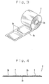
- Fig. 3 is a perspective view showing the label paper 2
- Fig. 4 is a cross-sectional view showing the label paper 2.
- the label paper 2 has many printing label 2b on a base paper 2a.
- a RF tag T is embedded in the printing label 2b held on the label paper 2.
- the RF tag T and the printing label 2b are integral and are removable from the base paper 2a after printing to be affixed on an object.
- the RF tag T is used for RFID and is also called an IC tag.
- the RF tag T which is not shown in detail, mainly comprises an IC chip including a storing part for storing ID data or other data and an antenna capable of transmitting data by radio communication. Electrostatic coupling type, electromagnetic coupling type, electromagnetic induction type, microwave type or other type can be applied to communication type between the RF tag reader/writer and the RF tag.
- CPU 11 executes printing on the printing label 2b of the label paper 2 in the main scanning direction by selectively electrically heating the resistance heating elements arranged in a line in the thermal head 5 in accordance with printing data which is input through the communication I/F 16 so as to melt or sublime an ink of the ink ribbon 4.
- CPU 11 also executes printing in the sub scanning direction by moving the label paper 2 with respect to the thermal head 5 in the conveying direction A (shown in Fig. 1) by rotating of the platen roller 3, which is driven by the stepping motor 15.
- CPU 11 rotates and drives the ink ribbon 4 by a drive force of the stepping motor 15 and rolls up used ink ribbon 4 on a reel shaft 4a.
- a printing part of the label printer of the present invention comprises the platen roller 3, the ink ribbon 4 and the thermal head 5, and a conveying mechanism comprises the platen roller 3 and the stepping motor 15.
- CPU 11 writes data which is input through the communication I/F 16 on the RF tag T embedded in the printing label 2b by the RF tag reader/writer 7 when the RF tag passes above the slit S in the conveyance plate 9.
- the RF tag reader/writer 7 and a structure arranged proximately thereto will now be described in detail.
- Fig. 5 is an exploded perspective view showing a structure near a RF tag reader/writer 7.
- a dielectric component 8 and the conveyance plate 9 are disposed on the antenna 7a of the RF tag reader/writer.
- the antenna 7a, the dielectrics component 8 and the conveyance plate 9 can be integrally formed as the RF tag reader/writer, or the dielectrics component 8 and the conveyance plate 9 can be arranged later on the antenna 7a of the RF tag reader/writer 7.
- Fig. 6 is a plan view showing a relationship between the conveyance plate 9 and the RF tag T in the label paper 2.
- the base paper 2a of the label paper 2 is conveyed on the conveyance surface of the conveyance plate 9.
- a slit S as a radio wave passage is formed in an approximately central portion of the conveyance plate 9.
- a longitudinal direction of the antenna 7a and the slit S is approximately perpendicular to the conveying direction A of the label paper 2.
- the antenna 7a is disposed under the dielectric component 8 below the slit S.
- the antenna 7a is arranged in a location opposite to an area where the RF tag T passes, and transmits and receives radio waves.
- the antenna 7a has a directivity towards the RF tag T in the label paper 2 in such a direction that an output radio wave is stronger.
- Fig.7 is a plan view showing a shape of an antenna of the RF tag reader/writer.
- the antenna 7a of the RF tag reader/writer 7 comprises a circuit board.
- the shaded portion in Fig.7 is a copper foil pattern.
- the entire back side of the antenna 7a is ground, and the antenna 7a outputs radio waves strongly in the direction of coming out of the sheet of Fig. 7.
- a core of coaxial cable 20 is connected to a feeding point X at an end of the pattern of the surface of the antenna 7a, and an external conductor of the coaxial cable 20 is connected to the backside ground.
- the other end of the coaxial cable 20 is connected to the transmitter/receiver 7d (shown in Fig. 2) which controls radio communication and other functions.
- the high frequency wave When a high frequency wave provided from the feeding point X is radiated from a first radiation element 21 to the air as a radio wave, the high frequency wave excites a second radiation element 22 and a third radiation element 23 arranged parallel with the first radiation element 21.
- lengths of the second radiation element 22 and the third radiation element 23 are longer than that of the first radiation element 21, and the second radiation element 22 and the third radiation element 23 resonate with a lower frequency than the first radiation element 21 does. Accordingly, a range of frequencies of the antenna 7a can be broadened. The range of frequencies can be further broadened by increasing a number of radiation elements having different lengths. The influence of objects around the antenna 7a can be reduced by broadening a ground part of the antenna 7a.
- the radiation elements and the slit S it becomes difficult to broaden the range of frequencies when a width of an area where the radiation elements are arranged in the conveying direction A is wider than a width of the slit S of the conveyance plate 9, such that the radiation elements and a metal portion of the conveyance plate 9 overlap. It is therefore preferable for the radiation elements and the slit S to have a similar width and shape, and for the ground and the conveyance plate 9 to have a similar width to make the external shape of the antenna 7a broader than that of the slit S of the conveyance plate 9.
- a projection 30 is formed in the approximately central portion of the dielectric component 8 which is arranged below the conveyance plate 9.
- the projection 30 is inserted into the slit S of the conveyance plate 9 from below.
- an upper surface of the projection 30 and an upper surface of the conveyance plate 9 are in the same plane.
- the upper surface of the projection 30 therefore forms the conveyance surface of the base paper 2a of the label paper 2 in a similar way as the upper surface of the conveyance plate 9.
- the structure explained above serves to eliminate an uneven conveyance surface of the base paper 2a of the label paper 2 and to prevent the base paper 2a of the label paper 2 from jamming and from winding.
- a radio wave has a property that its wavelength in the dielectric component 8 is shorter than its wavelength in free space.
- ⁇ 0 is a wavelength in free air
- ⁇ R is relative permeability
- ⁇ R is relative permittivity.
- relative permeability ⁇ R is 1, thus the wavelength ⁇ is shorter as the relative permittivity ⁇ R is higher.
- the RF tag reader/writer having the structure described above radiates a transmission signal from the transmitter/receiver 7d as a radio wave from the antenna 7a. Also, the RF tag reader/writer 7 transmits a signal to the transmitter/receiver 7d when the RF tag reader/writer 7 receives a radio wave from the RF tag T by the antenna 7a and the transmitter/receiver 7d extracts information from the received signal.
- a radio wave radiated from the antenna 7a passes the slit S of the conveyance plate 9 and arrives at the RF tag T provided in the printing label 2b of the label paper 2 passing over the slit S. Further, since the radio wave radiated from the RF tag T passes through the slit S to arrive at the antenna 7a, the communication with the RF tag T can be performed effectively.
- the RF tag reader/writer of the embodiment of the present invention by arranging a plurality of radiation elements having different lengths to broaden the range of frequencies of the antenna, effective communication can be achieved even if a frequency range used in radio communication is wide or various frequencies are used.
- the longitudinal length of the antenna 7a of the RF tag reader/writer can be decreased.
- the embodiment of the present invention is described in conjunction with a specific structure in which the dielectric component 8 is inserted into the slit S of the conveyance plate 9, but the present invention is not limited to this structure.
- the internal part of the slit S can be the air, that is, can be an air layer instead of the dielectrics component 8.
- the shape of the slit S is similar to the shape of the antenna of the RF tag T as much as possible because the base paper 2a of the label paper 2 is apt to jam on if the width of the slit S is broad.
Landscapes
- Engineering & Computer Science (AREA)
- Physics & Mathematics (AREA)
- Health & Medical Sciences (AREA)
- Toxicology (AREA)
- Theoretical Computer Science (AREA)
- General Physics & Mathematics (AREA)
- Computer Networks & Wireless Communication (AREA)
- Computer Vision & Pattern Recognition (AREA)
- Artificial Intelligence (AREA)
- General Health & Medical Sciences (AREA)
- Electromagnetism (AREA)
- General Engineering & Computer Science (AREA)
- Accessory Devices And Overall Control Thereof (AREA)
- Details Of Aerials (AREA)
- Printers Characterized By Their Purpose (AREA)
- Record Information Processing For Printing (AREA)
Abstract
Description
- The present invention relates to a RF tag reader/writer for reading and writing of a RF tag.
- A technology called RFID (Radio Frequency Identification) is currently widely popular. A RF tag also called an IC tag is used in an application of the RFID. A RF tag can be read and data can be written thereto without contact by use of radio waves. Reading and writing of a RF tag is possible even if the tag itself is hidden.
- A label type RF tag contained in a printable label is known. A RF tag label printer which is capable of reading and writing information on a label type RF tag by radio communication and which is capable of printing on a surface of a label containing the RF tag therein is described in Japanese Patent Laid-Open Publication No. 2001-96814. A device having a function of reading and writing information on a RF tag by radio communication is a RF tag reader/writer.
- Currently, an internal space of a label printer has been made smaller due to miniaturization of the label printer. Thus, when a RF tag reader/writer is contained in a miniaturized label printer, the RF tag reader/writer tends to be located near a conveyance plate having a conveyance surface for conveying a paper. In some instances, the conveyance plate may stand between the RF tag reader/writer and the RF tag. Since the conveyance plate is often made of metal, a radio wave used in radio communication is susceptible to the metal. Thus when the conveyance plate is positioned between the RF tag reader/writer and the RF tag, there is a problem that the communication between the RF tag reader/writer and the RF tag may be impeded because a radio wave being transmitted to and received by an antenna of the RF tag reader/writer is shielded by the conveyance plate.
- An object of the present invention is to enable effective communication between a RF tag reader/writer and a RF tag.
- Another object of the present invention is to miniaturize the RF tag reader/writer.
- According to the present invention, a RF tag reader/writer is provided which includes: (i) a conveyance plate including a conveyance surface for conveying a paper containing a RF tag, (ii) an antenna having a radiation element wherein the radiation element is positioned such that the RF tag provided in the paper conveyed on the conveyance surface passes over the radiation element, and (iii) a communication section for transmitting and receiving radio waves to and from the RF tag through the antenna so as to execute data communication with the RF tag. In addition, a radio wave passage is provided in the conveyance plate at a position corresponding to the antenna such that the radio waves between the antenna and the RF tag pass through the radio wave passage.
- A more complete appreciation of the present invention and many of the attendant advantages thereof will be readily obtained as the same becomes better understood by reference to the following detailed description when considered in connection with the accompanying drawings, wherein:
- Fig. 1 is a side view in vertical section schematically showing structure of a label printer according to an embodiment of the present invention;
- Fig. 2 is a block diagram showing an electrical connection of each part of the label printer according to the embodiment of the present invention;
- Fig. 3 is a perspective view of a label paper used in the label printer according to the embodiment of the present invention;
- Fig. 4 is a cross-sectional view of the label paper used in the label printer according to the embodiment of the present invention;
- Fig. 5 is an exploded perspective view showing a structure near the RF tag reader/writer;
- Fig. 6 is a plan view showing a relationship between the conveyance plate and the RF tag on the label paper; and
- Fig. 7 is a plan view showing a shape of an antenna of the RF tag reader/writer.
-
- An embodiment of the present invention will be described with reference to Fig. 1 to Fig. 7. A printing apparatus according to this embodiment of the present invention is applied to a label printer.
- Fig. 1 is a side view in vertical section schematically showing a structure of a
label printer 1. As shown in Fig. 1, a platen roller 3 pulls out alabel paper 2 which is rolled about areel shaft 2c (see Fig. 3) and conveys thelabel paper 2 in a conveying direction A. An ink ribbon 4 and athermal head 5, which is a printing head for printing a predetermined matter through the ink ribbon 4 on thelabel paper 2 pulled out from the roll, are disposed opposite to the platen roller 3. Thethermal head 5 includes many resistance heating elements (not shown) arranged in a line. The ink ribbon 4 is disposed to contact thethermal head 5 with pressure so that the ink ribbon 4 presses thelabel paper 2 against the platen roller 3. - In the
label printer 1, a RF tag reader/writer 7 is provided for writing or reading information on a RF tag T (shown in Fig. 4) provided in thelabel paper 2. - A transmitter/
receiver 7d as a communication section of the RF tag reader/writer 7 for writing or reading information on the RF tag T (shown in Fig. 4) is provided (not shown). - Fig. 2 is a block diagram showing an electrical connection of each part of the
label printer 1. In thelabel printer 1, aCPU 11 for controlling each part intensively is provided in thelabel printer 1 as shown in Fig. 2. AROM 13 comprising a flash memory is connected to asystem bus 12 from theCPU 11. Various programs for operating thelabel printer 1 are stored in theROM 13. That is, theROM 13 is a storage medium to store programs. In addition, aRAM 14 which is a storing part functioning as a working area for various operation such as retrieving the programs stored in theROM 13 is also connected to thesystem bus 12 from theCPU 11.CPU 11 executes various types of processing according to the programs stored in theROM 13 while utilizing theRAM 14 as a working area. Athermal head 5, a RF tag reader/writer 7, astepping motor 15 for conveying the ink ribbon 4 while conveying thelabel paper 2 by rotating the platen roller 3, and a communication interface (I/F) 16 for inputting data to be stored on the RF tag T or printing data output from a external device are also connected to thesystem bus 12 from theCPU 11. - The
label paper 2 used in thelabel printer 1 will now be described with respect to Figs. 3 and 4. Fig. 3 is a perspective view showing thelabel paper 2, and Fig. 4 is a cross-sectional view showing thelabel paper 2. As shown in Fig. 3, thelabel paper 2 hasmany printing label 2b on abase paper 2a. As shown in Fig. 4, a RF tag T is embedded in theprinting label 2b held on thelabel paper 2. The RF tag T and theprinting label 2b are integral and are removable from thebase paper 2a after printing to be affixed on an object. The RF tag T is used for RFID and is also called an IC tag. The RF tag T, which is not shown in detail, mainly comprises an IC chip including a storing part for storing ID data or other data and an antenna capable of transmitting data by radio communication. Electrostatic coupling type, electromagnetic coupling type, electromagnetic induction type, microwave type or other type can be applied to communication type between the RF tag reader/writer and the RF tag. - A basic processing operation by
CPU 11 of thelabel printer 1 will now be described.CPU 11 executes printing on theprinting label 2b of thelabel paper 2 in the main scanning direction by selectively electrically heating the resistance heating elements arranged in a line in thethermal head 5 in accordance with printing data which is input through the communication I/F 16 so as to melt or sublime an ink of the ink ribbon 4.CPU 11 also executes printing in the sub scanning direction by moving thelabel paper 2 with respect to thethermal head 5 in the conveying direction A (shown in Fig. 1) by rotating of the platen roller 3, which is driven by thestepping motor 15.CPU 11 rotates and drives the ink ribbon 4 by a drive force of the steppingmotor 15 and rolls up used ink ribbon 4 on a reel shaft 4a. Thus, a printing part of the label printer of the present invention comprises the platen roller 3, the ink ribbon 4 and thethermal head 5, and a conveying mechanism comprises the platen roller 3 and thestepping motor 15. - The
label paper 2, which is conveyed in the conveying direction A (shown in Fig. 1) for printing, passes above a slit S of theconveyance plate 9 while being conveyed.CPU 11 writes data which is input through the communication I/F 16 on the RF tag T embedded in theprinting label 2b by the RF tag reader/writer 7 when the RF tag passes above the slit S in theconveyance plate 9. - The RF tag reader/
writer 7 and a structure arranged proximately thereto will now be described in detail. - Fig. 5 is an exploded perspective view showing a structure near a RF tag reader/
writer 7. As shown in Fig. 5, adielectric component 8 and theconveyance plate 9 are disposed on theantenna 7a of the RF tag reader/writer. Theantenna 7a, thedielectrics component 8 and theconveyance plate 9 can be integrally formed as the RF tag reader/writer, or thedielectrics component 8 and theconveyance plate 9 can be arranged later on theantenna 7a of the RF tag reader/writer 7. - Fig. 6 is a plan view showing a relationship between the
conveyance plate 9 and the RF tag T in thelabel paper 2. As shown in Fig. 6, thebase paper 2a of thelabel paper 2 is conveyed on the conveyance surface of theconveyance plate 9. A slit S as a radio wave passage is formed in an approximately central portion of theconveyance plate 9. A longitudinal direction of theantenna 7a and the slit S is approximately perpendicular to the conveying direction A of thelabel paper 2. Theantenna 7a is disposed under thedielectric component 8 below the slit S. Theantenna 7a is arranged in a location opposite to an area where the RF tag T passes, and transmits and receives radio waves. Theantenna 7a has a directivity towards the RF tag T in thelabel paper 2 in such a direction that an output radio wave is stronger. - Fig.7 is a plan view showing a shape of an antenna of the RF tag reader/writer. As shown in Fig. 7, the
antenna 7a of the RF tag reader/writer 7 comprises a circuit board. The shaded portion in Fig.7 is a copper foil pattern. The entire back side of theantenna 7a is ground, and theantenna 7a outputs radio waves strongly in the direction of coming out of the sheet of Fig. 7. A core ofcoaxial cable 20 is connected to a feeding point X at an end of the pattern of the surface of theantenna 7a, and an external conductor of thecoaxial cable 20 is connected to the backside ground. The other end of thecoaxial cable 20 is connected to the transmitter/receiver 7d (shown in Fig. 2) which controls radio communication and other functions. When a high frequency wave provided from the feeding point X is radiated from afirst radiation element 21 to the air as a radio wave, the high frequency wave excites asecond radiation element 22 and athird radiation element 23 arranged parallel with thefirst radiation element 21. In theantenna 7a of the embodiment of the present invention, lengths of thesecond radiation element 22 and thethird radiation element 23 are longer than that of thefirst radiation element 21, and thesecond radiation element 22 and thethird radiation element 23 resonate with a lower frequency than thefirst radiation element 21 does. Accordingly, a range of frequencies of theantenna 7a can be broadened. The range of frequencies can be further broadened by increasing a number of radiation elements having different lengths. The influence of objects around theantenna 7a can be reduced by broadening a ground part of theantenna 7a. - It becomes difficult to broaden the range of frequencies when a width of an area where the radiation elements are arranged in the conveying direction A is wider than a width of the slit S of the
conveyance plate 9, such that the radiation elements and a metal portion of theconveyance plate 9 overlap. It is therefore preferable for the radiation elements and the slit S to have a similar width and shape, and for the ground and theconveyance plate 9 to have a similar width to make the external shape of theantenna 7a broader than that of the slit S of theconveyance plate 9. - A
projection 30 is formed in the approximately central portion of thedielectric component 8 which is arranged below theconveyance plate 9. Theprojection 30 is inserted into the slit S of theconveyance plate 9 from below. When thedielectric component 8 is pressed into theconveyance plate 9 from below, an upper surface of theprojection 30 and an upper surface of theconveyance plate 9 are in the same plane. The upper surface of theprojection 30 therefore forms the conveyance surface of thebase paper 2a of thelabel paper 2 in a similar way as the upper surface of theconveyance plate 9. - The structure explained above serves to eliminate an uneven conveyance surface of the
base paper 2a of thelabel paper 2 and to prevent thebase paper 2a of thelabel paper 2 from jamming and from winding. - A radio wave has a property that its wavelength in the
dielectric component 8 is shorter than its wavelength in free space. Generally, the wavelength λ in thedielectrics component 8 is expressed as the following formula (1) ;dielectrics component 8, the longitudinal length of theantenna 7a of the RF tag reader/writer can be shorter so that theantenna 7a can be miniaturized. - The RF tag reader/writer having the structure described above radiates a transmission signal from the transmitter/
receiver 7d as a radio wave from theantenna 7a. Also, the RF tag reader/writer 7 transmits a signal to the transmitter/receiver 7d when the RF tag reader/writer 7 receives a radio wave from the RF tag T by theantenna 7a and the transmitter/receiver 7d extracts information from the received signal. - According to the RF tag reader/writer of the embodiment of the present invention, a radio wave radiated from the
antenna 7a passes the slit S of theconveyance plate 9 and arrives at the RF tag T provided in theprinting label 2b of thelabel paper 2 passing over the slit S. Further, since the radio wave radiated from the RF tag T passes through the slit S to arrive at theantenna 7a, the communication with the RF tag T can be performed effectively. - According to the RF tag reader/writer of the embodiment of the present invention, by arranging a plurality of radiation elements having different lengths to broaden the range of frequencies of the antenna, effective communication can be achieved even if a frequency range used in radio communication is wide or various frequencies are used.
- In addition, according to the RF tag reader/writer of the embodiment, by arranging the
dielectrics component 8 on theantenna 7a, the longitudinal length of theantenna 7a of the RF tag reader/writer can be decreased. - The embodiment of the present invention is described in conjunction with a specific structure in which the
dielectric component 8 is inserted into the slit S of theconveyance plate 9, but the present invention is not limited to this structure. The internal part of the slit S can be the air, that is, can be an air layer instead of thedielectrics component 8. In this case it is preferable that the shape of the slit S is similar to the shape of the antenna of the RF tag T as much as possible because thebase paper 2a of thelabel paper 2 is apt to jam on if the width of the slit S is broad. - It is explicitly stated that all features disclosed in the description and/or the claims are intended to be disclosed separately and independently from each other for the purpose of original disclosure as well as for the purpose of restricting the claimed invention independent of the composition of the features in the embodiments and/or the claims. It is explicitly stated that all value ranges or indications of groups of entities disclose every possible intermediate value or intermediate entity for the purpose of original disclosure as well as for the purpose of restricting the claimed invention, in particular as limits of value ranges.
Claims (9)
- A RF tag reader/writer (7) for reading and writing information on a RF tag (T) provided in a paper (2), comprising:characterized in that it is provided a radio wave passage (S) provided in the conveyance plate at a position corresponding to the antenna such that the radio waves between the antenna and the RF tag pass through the radio wave passage.a conveyance plate(9) including a conveyance surface for conveying the paper containing the RF tag;an antenna (7a) including a radiation element(21, 22, 23), the radiation element being positioned such that the RF tag provided in the paper conveyed on the conveyance surface passes over the radiation element; anda communication section (7d) for transmitting and receiving radio waves to and from the RF tag through the antenna so as to execute data communication with the RF tag,
- The RF tag reader/writer according to claim 1, wherein the radio wave passage has substantially a same shape as an external shape of the antenna, and has substantially a same size as the antenna.
- The RF tag reader/writer according to claim 1, wherein the radio wave passage is slightly smaller than the antenna.
- The RF tag reader/writer according to claims 1, 2 or 3, wherein the radiation element comprises a plurality of radiation elements and at least two of the radiation elements have different lengths.
- The RF tag reader/writer according to claims 1, 2, 3 or 4, wherein longitudinal directions of the antenna and the radio wave passage are substantially perpendicular to a paper conveying direction.
- The RF tag reader/writer according to claims 1, 2, 3, 4 or 5, wherein the antenna has a directivity towards the RF tag provided in the paper conveyed on the conveyance plate.
- The RF tag reader/writer according to claims 1, 2, 3, 4, 5 or 6, further comprising a dielectric component inserted in the radio wave passage of the conveyance plate.
- The RF tag reader/writer according to claim 7, wherein an upper surface of the dielectric component inserted in the radio wave passage is in a same plane as the conveyance surface of the conveyance plate.
- A printer, comprising:a paper conveyer (3, 15) for conveying a paper containing a RF tag;a printing member (3, 4, 5) for printing on the paper; anda RF tag reader/writer (7) for reading and writing information on the RF tag provided in the paper conveyed by the paper conveyer defined in any one of claims 1, 2, 3, 4, 5, 6, 7 or 8.
Applications Claiming Priority (2)
| Application Number | Priority Date | Filing Date | Title |
|---|---|---|---|
| JP2004134513A JP3935162B2 (en) | 2004-04-28 | 2004-04-28 | RF tag reader / writer and printer |
| JP2004134513 | 2004-04-28 |
Publications (3)
| Publication Number | Publication Date |
|---|---|
| EP1591946A2 true EP1591946A2 (en) | 2005-11-02 |
| EP1591946A3 EP1591946A3 (en) | 2007-04-04 |
| EP1591946B1 EP1591946B1 (en) | 2011-01-26 |
Family
ID=34935667
Family Applications (1)
| Application Number | Title | Priority Date | Filing Date |
|---|---|---|---|
| EP05008990A Expired - Lifetime EP1591946B1 (en) | 2004-04-28 | 2005-04-25 | RF tag reader/writer and printer containing the RF tag reader/writer |
Country Status (5)
| Country | Link |
|---|---|
| US (1) | US7327265B2 (en) |
| EP (1) | EP1591946B1 (en) |
| JP (1) | JP3935162B2 (en) |
| CN (1) | CN1689825B (en) |
| DE (1) | DE602005026080D1 (en) |
Cited By (2)
| Publication number | Priority date | Publication date | Assignee | Title |
|---|---|---|---|---|
| EP1850268A3 (en) * | 2006-04-26 | 2008-07-23 | Toshiba TEC Kabushiki Kaisha | Radio-communication apparatus and method for enabling radio-communication between radio-communication apparatus and data carrier |
| EP4006779A1 (en) * | 2020-11-25 | 2022-06-01 | Toshiba TEC Kabushiki Kaisha | Antenna and wireless tag issuing device |
Families Citing this family (18)
| Publication number | Priority date | Publication date | Assignee | Title |
|---|---|---|---|---|
| US7609406B2 (en) * | 2002-08-16 | 2009-10-27 | Avery Dennison Retail Information Services, Llc | Hand held portable printer with RFID read write capability |
| US7398926B1 (en) * | 2003-10-06 | 2008-07-15 | Applied Wireless Identifications Group, Inc. | Apparatus and method for programming an RFID transponder using a constrained field |
| US20050116034A1 (en) * | 2003-11-28 | 2005-06-02 | Masato Satake | Printing system |
| JP4268514B2 (en) * | 2003-12-25 | 2009-05-27 | 東芝テック株式会社 | Wireless tag issuing device |
| JP2006209497A (en) * | 2005-01-28 | 2006-08-10 | Seiko Epson Corp | RFID tag, printing paper, printer device, RFID system |
| US7926722B2 (en) * | 2005-03-03 | 2011-04-19 | Toshiba Tec Kabushiki Kaisha | Printer and IC chip communication apparatus |
| JP4208855B2 (en) * | 2005-04-08 | 2009-01-14 | キヤノン株式会社 | Sheet conveying apparatus and image forming apparatus |
| EP1942444B1 (en) * | 2006-11-28 | 2014-03-19 | Brother Kogyo Kabushiki Kaisha | RFID tag information communicating apparatus |
| TWI341494B (en) * | 2007-02-07 | 2011-05-01 | Mstar Semiconductor Inc | Label paper with rfid function and rfid tag writing apparatus |
| JP2009083459A (en) * | 2007-09-10 | 2009-04-23 | Toshiba Tec Corp | Label printer, computer program for label printer, computer program, and data transmission method |
| JP2009199454A (en) * | 2008-02-22 | 2009-09-03 | Toshiba Tec Corp | Radio tag issuing device |
| US8313187B2 (en) * | 2008-04-30 | 2012-11-20 | Lexmark International, Inc. | Modular RFID imaging device option |
| JP2015123615A (en) * | 2013-12-25 | 2015-07-06 | 東芝テック株式会社 | Rfid tag issuing device |
| JP2018198036A (en) | 2017-05-25 | 2018-12-13 | 東芝テック株式会社 | Label processor |
| JP7062454B2 (en) * | 2018-02-05 | 2022-05-16 | 東芝テック株式会社 | Label issuing device and antenna |
| US11247486B1 (en) * | 2019-04-23 | 2022-02-15 | CMSI Technologies | Tag printer apparatus |
| EP4096608A4 (en) * | 2020-03-12 | 2024-02-14 | Raja Tuli | Remote incontinence monitoring system using a plurality of re tags associated with dedicated frequencies |
| JP7443178B2 (en) | 2020-07-16 | 2024-03-05 | 東芝テック株式会社 | Wireless tag communication device and sheet processing device |
Citations (4)
| Publication number | Priority date | Publication date | Assignee | Title |
|---|---|---|---|---|
| WO1999021144A1 (en) | 1997-10-20 | 1999-04-29 | Escort Memory Systems | Rfid conveyor antenna |
| US6104291A (en) | 1998-01-09 | 2000-08-15 | Intermec Ip Corp. | Method and apparatus for testing RFID tags |
| JP2003132330A (en) | 2001-10-25 | 2003-05-09 | Sato Corp | RFID label printer |
| US6593853B1 (en) | 2000-02-18 | 2003-07-15 | Brady Worldwide, Inc. | RFID label printing system |
Family Cites Families (11)
| Publication number | Priority date | Publication date | Assignee | Title |
|---|---|---|---|---|
| JPH0669715A (en) | 1992-08-17 | 1994-03-11 | Nippon Mektron Ltd | Broadband linear antenna |
| JP2916474B1 (en) | 1998-06-03 | 1999-07-05 | 八木アンテナ株式会社 | Label writing head |
| JP2000105800A (en) | 1998-09-29 | 2000-04-11 | Toshiba Corp | Wireless communication media processing device |
| DE19846295B4 (en) * | 1998-10-07 | 2008-04-24 | Kabushiki Kaisha Sato | Printer with a device for driving transponder chips |
| JP2001096814A (en) | 1999-09-29 | 2001-04-10 | Toshiba Tec Corp | Printer with RF-ID reading / writing device |
| JP4545280B2 (en) | 2000-05-24 | 2010-09-15 | 株式会社サトー | Printer |
| JP4514374B2 (en) | 2001-09-05 | 2010-07-28 | トッパン・フォームズ株式会社 | RF-ID inspection system |
| JP2003338705A (en) | 2002-05-22 | 2003-11-28 | Hitachi Ltd | Article information reading method and apparatus |
| US6848616B2 (en) * | 2003-03-11 | 2005-02-01 | Zih Corp., A Delaware Corporation With Its Principal Office In Hamilton, Bermuda | System and method for selective communication with RFID transponders |
| US7398054B2 (en) * | 2003-08-29 | 2008-07-08 | Zih Corp. | Spatially selective UHF near field microstrip coupler device and RFID systems using device |
| US20050058483A1 (en) * | 2003-09-12 | 2005-03-17 | Chapman Theodore A. | RFID tag and printer system |
-
2004
- 2004-04-28 JP JP2004134513A patent/JP3935162B2/en not_active Expired - Fee Related
-
2005
- 2005-04-25 EP EP05008990A patent/EP1591946B1/en not_active Expired - Lifetime
- 2005-04-25 DE DE602005026080T patent/DE602005026080D1/en not_active Expired - Lifetime
- 2005-04-26 US US11/114,956 patent/US7327265B2/en not_active Expired - Fee Related
- 2005-04-28 CN CN200510068459.6A patent/CN1689825B/en not_active Expired - Fee Related
Patent Citations (4)
| Publication number | Priority date | Publication date | Assignee | Title |
|---|---|---|---|---|
| WO1999021144A1 (en) | 1997-10-20 | 1999-04-29 | Escort Memory Systems | Rfid conveyor antenna |
| US6104291A (en) | 1998-01-09 | 2000-08-15 | Intermec Ip Corp. | Method and apparatus for testing RFID tags |
| US6593853B1 (en) | 2000-02-18 | 2003-07-15 | Brady Worldwide, Inc. | RFID label printing system |
| JP2003132330A (en) | 2001-10-25 | 2003-05-09 | Sato Corp | RFID label printer |
Cited By (3)
| Publication number | Priority date | Publication date | Assignee | Title |
|---|---|---|---|---|
| EP1850268A3 (en) * | 2006-04-26 | 2008-07-23 | Toshiba TEC Kabushiki Kaisha | Radio-communication apparatus and method for enabling radio-communication between radio-communication apparatus and data carrier |
| EP4006779A1 (en) * | 2020-11-25 | 2022-06-01 | Toshiba TEC Kabushiki Kaisha | Antenna and wireless tag issuing device |
| US11544482B2 (en) | 2020-11-25 | 2023-01-03 | Toshiba Tec Kabushiki Kaisha | Antenna and wireless tag issuing device |
Also Published As
| Publication number | Publication date |
|---|---|
| JP2005316767A (en) | 2005-11-10 |
| DE602005026080D1 (en) | 2011-03-10 |
| CN1689825A (en) | 2005-11-02 |
| JP3935162B2 (en) | 2007-06-20 |
| EP1591946A3 (en) | 2007-04-04 |
| US20050252968A1 (en) | 2005-11-17 |
| CN1689825B (en) | 2010-05-12 |
| EP1591946B1 (en) | 2011-01-26 |
| US7327265B2 (en) | 2008-02-05 |
Similar Documents
| Publication | Publication Date | Title |
|---|---|---|
| US7327265B2 (en) | RF tag reader/writer and printer containing the RF tag reader/writer | |
| US11062193B2 (en) | Encoding module, associated encoding element, connector, printer-encoder and access control system | |
| USRE44631E1 (en) | Radio tag issuing apparatus and tag issuing method | |
| JP3867085B2 (en) | Wireless communication device, RF tag reader / writer, and printer | |
| US9108434B2 (en) | RFID near-field antenna and associated systems | |
| US8351959B2 (en) | Spatially selective UHF near field microstrip coupler device and RFID systems using device | |
| US8358246B2 (en) | RFID UHF stripline antenna-coupler | |
| US8791874B2 (en) | Near field coupling devices and associated systems and methods | |
| US7425887B2 (en) | Multi-layered efficient RFID coupler | |
| US7839287B2 (en) | Near-field miniature coupler | |
| EP3790108B1 (en) | Antenna and rfid tag issuing apparatus | |
| JP2010165150A (en) | Antenna device for rfid reader/writer, and rfid tag issuing device | |
| CN104751207A (en) | RFID tag issuing device | |
| JP2019135612A (en) | Label issuing device and antenna | |
| JP2005332318A (en) | Wireless communication apparatus and printer | |
| JP4932859B2 (en) | Wireless tag issuing device | |
| KR20060133402A (en) | Meandered Slit Antenna | |
| JP2005333556A (en) | Antenna, wireless communication device and printer |
Legal Events
| Date | Code | Title | Description |
|---|---|---|---|
| PUAI | Public reference made under article 153(3) epc to a published international application that has entered the european phase |
Free format text: ORIGINAL CODE: 0009012 |
|
| 17P | Request for examination filed |
Effective date: 20050425 |
|
| AK | Designated contracting states |
Kind code of ref document: A2 Designated state(s): AT BE BG CH CY CZ DE DK EE ES FI FR GB GR HU IE IS IT LI LT LU MC NL PL PT RO SE SI SK TR |
|
| AX | Request for extension of the european patent |
Extension state: AL BA HR LV MK YU |
|
| PUAL | Search report despatched |
Free format text: ORIGINAL CODE: 0009013 |
|
| AK | Designated contracting states |
Kind code of ref document: A3 Designated state(s): AT BE BG CH CY CZ DE DK EE ES FI FR GB GR HU IE IS IT LI LT LU MC NL PL PT RO SE SI SK TR |
|
| AX | Request for extension of the european patent |
Extension state: AL BA HR LV MK YU |
|
| AKX | Designation fees paid |
Designated state(s): DE FR GB |
|
| 17Q | First examination report despatched |
Effective date: 20090608 |
|
| GRAP | Despatch of communication of intention to grant a patent |
Free format text: ORIGINAL CODE: EPIDOSNIGR1 |
|
| GRAS | Grant fee paid |
Free format text: ORIGINAL CODE: EPIDOSNIGR3 |
|
| GRAA | (expected) grant |
Free format text: ORIGINAL CODE: 0009210 |
|
| AK | Designated contracting states |
Kind code of ref document: B1 Designated state(s): DE FR GB |
|
| REG | Reference to a national code |
Ref country code: GB Ref legal event code: FG4D |
|
| REF | Corresponds to: |
Ref document number: 602005026080 Country of ref document: DE Date of ref document: 20110310 Kind code of ref document: P |
|
| REG | Reference to a national code |
Ref country code: DE Ref legal event code: R096 Ref document number: 602005026080 Country of ref document: DE Effective date: 20110310 |
|
| PGFP | Annual fee paid to national office [announced via postgrant information from national office to epo] |
Ref country code: DE Payment date: 20110420 Year of fee payment: 7 Ref country code: FR Payment date: 20110426 Year of fee payment: 7 |
|
| PGFP | Annual fee paid to national office [announced via postgrant information from national office to epo] |
Ref country code: GB Payment date: 20110420 Year of fee payment: 7 |
|
| PLBE | No opposition filed within time limit |
Free format text: ORIGINAL CODE: 0009261 |
|
| STAA | Information on the status of an ep patent application or granted ep patent |
Free format text: STATUS: NO OPPOSITION FILED WITHIN TIME LIMIT |
|
| 26N | No opposition filed |
Effective date: 20111027 |
|
| REG | Reference to a national code |
Ref country code: DE Ref legal event code: R097 Ref document number: 602005026080 Country of ref document: DE Effective date: 20111027 |
|
| GBPC | Gb: european patent ceased through non-payment of renewal fee |
Effective date: 20120425 |
|
| REG | Reference to a national code |
Ref country code: FR Ref legal event code: ST Effective date: 20121228 |
|
| PG25 | Lapsed in a contracting state [announced via postgrant information from national office to epo] |
Ref country code: GB Free format text: LAPSE BECAUSE OF NON-PAYMENT OF DUE FEES Effective date: 20120425 |
|
| REG | Reference to a national code |
Ref country code: DE Ref legal event code: R119 Ref document number: 602005026080 Country of ref document: DE Effective date: 20121101 |
|
| PG25 | Lapsed in a contracting state [announced via postgrant information from national office to epo] |
Ref country code: FR Free format text: LAPSE BECAUSE OF NON-PAYMENT OF DUE FEES Effective date: 20120430 |
|
| PG25 | Lapsed in a contracting state [announced via postgrant information from national office to epo] |
Ref country code: DE Free format text: LAPSE BECAUSE OF NON-PAYMENT OF DUE FEES Effective date: 20121101 |