BACKGROUND OF THE INVENTION
Field of the Invention
The present invention relates to a frequency output circuit for outputting a frequency
signal, and, in particular, to a frequency output circuit comprising an open-collector output
terminal.
Background Art
In order to reduce the emission of unwanted electromagnetic radiation from a
frequency output circuit, the circuit should ideally output a sine wave. JP Patent Publication
(Kokai) No. 2001-211047 A discloses that, in the case of a rectangular wave oscillator that is
not of the open-collector output configuration, a rectangular wave is shaped to be closer to a
sine wave using an inductor and a capacitor such that the unwanted electromagnetic radiation
can be eliminated.
In frequency output circuits with an open-collector output terminal, the transistor on
the output end is turned on or off and the signal voltage is received from an external power
supply, such that the waveform that is outputted is basically a rectangular wave. When the
output voltage occurs in the form of a rectangular wave, the current also flows through a
rectangular wave. As a result, a high-frequency electromagnetic wave is emitted, which can
have an influence on radios in terms of noise.
Therefore, in some known examples of the frequency output circuit with an
open-collector output terminal, a current mirror circuit is provided whereby the current that
flows through the open collector is limited.
Patent Document 1: JP Patent Publication (Kokai) No. 2001-211047 A
SUMMARY OF THE INVENTION
However, in the frequency output circuit with an open-collector output terminal that
is provided with a current mirror circuit, a current limit cannot be provided when the voltage
increases. Even when the voltage decreases, the voltage change is not smooth, making it
impossible to completely eliminate unwanted electromagnetic waves.
Meanwhile, in North America and Italy, there is a movement toward lowering the
lowest AM radio frequency from the current 450 kHz to 150 kHz so as to expand the AM band.
It has been found, however, that if the AM frequency is thus lowered, the unwanted
electromagnetic waves emitted from the frequency output circuit with an open-collector output
terminal, which previously had not been an issue, could provide radio noise.
It is therefore an object of the present invention to provide a frequency output circuit
with an open-collector output terminal whereby unwanted electromagnetic waves can be
eliminated and radio noise can be reduced.
In order to achieve the aforementioned object, the invention provides:
This configuration eliminates unwanted electromagnetic waves in a frequency output
circuit with an open-collector output terminal, thereby reducing radio noise.
(2) Preferably, in (1), the current limiting circuit comprises a differential pair circuit
of transistors each with a resistor provided in the emitter thereof, and a current mirror circuit
comprising an open-collector transistor. (3) Preferably, in (1), the current limiting circuit comprises a current mirror circuit
including a low-pass filter formed by a capacitor and a resistor. (4) Preferably, in (2) or (3), the transistors forming the current mirror circuit in the
current limiting circuit each comprise an adjusting resistor in the emitter thereof. (5) Preferably, in (2), signals inputted to the differential pair circuit of the current
limiting circuit comprise a triangular wave voltage signal with the same frequency as that of
an output signal, and a constant voltage signal with a value between the maximum voltage
value and the minimum voltage value of the triangular wave. (6) Preferably, in (2), signals inputted to the differential pair circuit of the current
limiting circuit comprise two kinds of triangular wave voltage signals with the same frequency
as that of an output signal and with different amplitudes. (7) Preferably, in (2), the differential pair circuit of the current limiting circuit
comprises a low-pass filter formed by a capacitor and a resistor at a signal input terminal
thereof. (8) Preferably, in (3), an input signal current inputted to the current mirror circuit in
the current limiting circuit comprises a triangular wave signal. (9) Preferably, in (3), the waveform of an input signal current inputted to the current
mirror circuit in the current limiting circuit comprises the waveform of a rectangular wave that
has been passed through the low-pass filter. (10) Preferably, in (1), there is further provided a pull-up resistor connected to the
open-collector output terminal and also connected to an internally provided reference power
supply.
In accordance with the invention, unwanted electromagnetic waves can be eliminated
in a frequency output circuit with an open-collector output terminal, so that radio noise can be
reduced.
BRIEF DESCRIPTION OF THE DRAWINGS
Fig. 1 shows a circuit diagram illustrating the configuration of a frequency output
circuit according to a first embodiment of the invention.
Fig. 2 shows an output characteristics chart of the frequency output circuit according
to the first embodiment of the invention.
Fig. 3 shows a circuit diagram illustrating the configuration of a current limiting
circuit 16 used in the frequency output circuit of the first embodiment.
Fig. 4 shows a characteristics chart of the frequency output circuit of the first
embodiment during current limitation.
Fig. 5 shows an operational chart of the frequency output circuit according to a
second embodiment of the invention.
Fig. 6 shows a circuit diagram illustrating the configuration of the frequency output
circuit according to a third embodiment of the invention.
Fig. 7 shows an operational waveform chart of the frequency output circuit of the
third embodiment.
Fig. 8 shows a circuit diagram illustrating the configuration of the frequency output
circuit according to a fourth embodiment of the invention.
Fig. 9 shows an operational waveform chart of the frequency output circuit of the
fourth embodiment.
Fig. 10 shows a circuit diagram illustrating the configuration of the frequency output
circuit according to a fifth embodiment of the invention.
Fig. 11 shows a circuit diagram of a current source used in the frequency output
circuit of the fifth embodiment.
Fig. 12 shows a circuit diagram illustrating the configuration of the frequency output
circuit according to a sixth embodiment of the invention.
Fig. 13 shows an operational waveform chart of the frequency output circuit of the
sixth embodiment.
Fig. 14 shows a circuit diagram illustrating the configuration of the frequency output
circuit according to a seventh embodiment of the invention.
DESCRIPTION OF THE PREFERRED EMBODIMENTS
Hereafter, the frequency output circuit according to a first embodiment of the present
invention will be described with reference to Figs. 1 to 4.
Initially referring to Figs. 1 and 2, the configuration and operation of the frequency
output circuit of the present embodiment will be described.
Fig. 1 shows a circuit diagram illustrating the configuration of the frequency output
circuit according to the first embodiment of the present invention. Fig. 2 shows an output
characteristics chart of the frequency output circuit of the first embodiment of the present
invention.
A frequency output circuit 10 comprises an output circuit 12, a current limiting circuit
16, and an open-collector transistor Q4. A triangular wave generating circuit 18 will be
described later. The output circuit 12 measures airflow rate, for example, as does a frequency
output-type airflow meter, and produces output that varies depending on the airflow rate.
Obviously, the output circuit 12 may be any device whose output is of the frequency type,
other than an airflow meter.
The output terminal of the frequency output circuit 10 is the collector of the
open-collector transistor Q4. The collector of transistor Q4 is connected to an external power
supply Vex of a signal-receiving external circuit 20 via a pull-up resistor Rf. Conventional
frequency output circuits are not provided with current limiting circuit 16. Instead, transistor
Q4 is turned ON and OFF using a frequency signal Va outputted by the output circuit 12.
When transistor Q4 is ON, an output current If flows through the collector of transistor Q4,
producing an output voltage Vfo, which is expressed by the following equation (1) and which
is on the lower potential side of the frequency output waveform:
Vfo = Vex - Rf × If
When transistor Q4 is OFF, no current flows through the collector of transistor Q4, so
that the output voltage Vfo becomes equal to Vex, which is on the higher voltage side of the
frequency output waveform. Thus, the output voltage Vfo takes the form of a rectangular
wave, leading to the emission of high-frequency electromagnetic wave radiation.
In contrast, in accordance with the present embodiment, there is a current limiting
circuit 16 provided between the output circuit 12 and transistor Q4. The current limiting
circuit 16 causes the output voltage Vfo of the frequency output circuit 10 to have a waveform
that is close to a sine wave in which harmonics components have been eliminated from the
rectangular frequency output waveform, as shown in Fig. 2. The current limiting circuit 16
limits the output current If that flows through transistor Q4 such that it does not change
sharply.
Now referring to Figs. 3 and 4, the circuit configuration and operation of the current
limiting circuit 16 will be described.
Fig. 3 shows a circuit diagram illustrating the configuration of the current limiting
circuit 16 used in the frequency output circuit according to the first embodiment of the
invention. Fig. 4 shows the characteristics of the frequency output circuit in the first
embodiment of the invention during current limitation. Similar reference characters indicate
similar elements in Figs. 1 and 3.
The current limiting circuit 16 comprises a differential pair of transistors Q1 and Q2,
with the gain lowered by providing resistors R1 and R2 to the emitters thereof, and a transistor
Q3 that forms a current mirror circuit with the open-collector transistor Q4. A signal Va that
is fed to transistor Q1 is a frequency signal. To transistor Q2, a constant potential Vc
between a maximum potential and a minimum potential of the frequency signal Va is fed.
Assuming that the currents that flow in the collectors of transistor Q1 and transistor Q2 are Ia
and Ic, respectively, and when R1 = R2 = Ra, the current that flows through the differential
pair will be described.
To the differential pair of transistor Q1 and Q2, a bias current Ib is applied. When
Va « Vc, the bias current Ib flows through transistor Q1. When Va = Vc, a current of Ib/2
flows through transistor Q1 and transistor Q2 individually. When Va » Vc, the bias current Ib
flows through transistor Q2. Since the differential pair consisting of transistors Q1 and Q2 is
a comparator with a very small gain, it has characteristics such that the output with respect to
the differential input signal does not change sharply. In order to reduce the gain of this
differential pair, resistors R1 and R2 are each provided with values on the order of 100 Ω for a
bias current Ib of 70 µA, for example.
Fig. 4 schematically shows the Va-Vc dependency of Ia and Ic. As shown in Fig. 4,
as the resistance Ra increases, the switching between currents Ia and Ic becomes more gradual.
Output current If is controlled by the current mirror circuit such that it is the same as current Ic.
Thus, the time when current If flows and the time when it stops are gradually switched.
With reference to the circuit diagram shown in Fig. 3, the relationship between
current If and voltages Va and Vc is described. Since the sum of currents Ia and Ib is equal to
bias current Ib, the following equation (2) holds:
Ia + Ic = Ib
The relationship between input voltages Va and Vc to the differential pair circuit
consisting of transistors Q1 and Q2 and currents Ia and Ic is expressed by the following
equation (3):
Va -Vc=Vt × Log (Ic/Ia) + Ra × (Ic - la)
where Vt is a thermal electromotive force, which is approximately 26 mV at 25°C.
Since Ic and If are equal because of the current mirror circuit consisting of transistors
Q3 and Q4, the following equation (4) holds:
Ic = If
From equations (2), (3), and (4), the relationship between If and Va and Vc can be
expressed by the following equation (5):
If = (Ib - If) × Exp ((Va - Vc + Ra × (Ib - 2 × If))/Vt)
Because equation (5) includes If on both sides, a convergent calculation is carried out
on a computer to determine the value.
When Va is a frequency signal and Vc is a constant voltage, the switching of the
output voltage Vfo can be made to take place gradually, as shown in Fig. 2, by increasing the
value of Ra and thereby resulting in the output characteristics of the differential pair, which
consists of transistors Q1 and Q2 and which is a comparator with a very small gain, such that
the output in response to a differential input signal is not sharply switched. In this way,
high-frequency components can be eliminated from the frequency output waveform and a
waveform close to a sine wave can be obtained, as shown in Fig. 2, whereby the influence of
radio noise can be reduced.
Thus, in accordance with the present embodiment, unwanted electromagnetic waves
can be eliminated in a frequency output circuit having an open-collector output terminal,
thereby reducing radio noise.
With reference to Figs. 1 and 5, the configuration of the frequency output circuit in
accordance with the second embodiment of the invention is described.
Fig. 5 shows the operation of the frequency output circuit in the second embodiment
of the invention.
The present embodiment characteristically comprises a triangular wave conversion
circuit 18, as shown in Fig. 1. The path directly leading from the output circuit 12 to the
current limiting circuit 16 is removed. The triangular wave conversion circuit 18 converts
the output of the output circuit 12, if it is a rectangular wave, into a triangular wave, as shown
in Fig. 5.
If Va is an ideal rectangular wave where the voltage switching time is zero, the
switching of the output voltage Vfo would also be sharp, as will be seen from Fig. 4 and
equation (5). This is due to the fact that the switching from Va « Vc to Va » Vc would be fast
and it would take only a short time before Va ≈ Vc. Although such an ideal rectangular wave
does not generally occur, the closer the voltage is to the ideal rectangular wave, the faster the
switching becomes. Accordingly, by converting a rectangular wave into a triangular wave
using the triangular wave conversion circuit 18, a time when Va ≈ Vc can be provided before
and after the time when Va = Vc in Fig. 5, so that the switching of the output voltage Vfo can
be made to take place gradually. In this way, high-frequency components can be eliminated
from the frequency output waveform and a waveform close to a sine wave can be obtained,
thereby reducing the noise influence on radio, for example.
While the triangular wave conversion circuit 18 has been separately provided, the
output circuit 12 per se may be configured such that it produces a triangular wave output.
In accordance with the above-described embodiment, unwanted electromagnetic
waves can be eliminated in a frequency output circuit having an open-collector output terminal,
so that radio noise can be reduced.
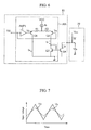
With reference to Figs. 6 and 7, the configuration of the frequency output circuit
according to a third embodiment will be described.
Fig. 6 shows a circuit diagram illustrating the configuration of the frequency output
circuit according to the third embodiment of the invention. Fig. 7 shows an operational
waveform chart of the frequency output circuit of the third embodiment. Similar reference
numerals designate similar elements in Figs. 1 and 3.
A current limiting circuit 16A includes an amplifier AMP1 connected to transistor Q1,
in addition to having the configuration shown in Fig. 3. An input signal Vd transmitted to the
current limiting circuit 16A is a frequency signal of a triangular wave. The frequency signal
Vd of the triangular wave has its amplitude changed by being amplified by the amplifier
AMP1 before being fed to the base of transistor Q1. The frequency signal Vd of the
triangular wave is also directly fed to the base of transistor Q2 as a reference signal Vc.
The relationship between voltages Va and Vc applied to the differential pair
consisting of transistors Q1 and Q2 is as shown in Fig. 7. Thus, the voltages Va and Vc
applied to the differential pair are both triangular waves and they gradually vary, such that the
time it takes for them to be approximately equal can be further increased. As a result, the
switching of output voltage Vfo can be made to take place gradually. In this way,
high-frequency components can be eliminated from the frequency output waveform and a
waveform close to a sine wave can be obtained, whereby the noise influence on radios, for
example, can be reduced.
As described above, in accordance with the present embodiment, the switching of the
output voltage can be made to take place gradually, whereby unwanted electromagnetic waves
can be eliminated and radio noise can be reduced.
With reference now to Figs. 8 and 9, the configuration of the frequency output circuit
according to a fourth embodiment of the invention will be described.
Fig. 8 shows a circuit diagram illustrating the configuration of the frequency output
circuit of the fourth embodiment. Fig. 9 shows an operational waveform chart of the
frequency output circuit of the fourth embodiment. Similar reference characters indicate
similar elements in Figs. 1 and 3:
The present embodiment includes a low-pass filter 14 in addition to the configuration
shown in Fig. 3. The low-pass filter 14 consists of a resistor R6 and a capacitor C1. By
supplying a rectangular wave output signal Vaa from output circuit 12 to the base of transistor
Q1 via low-pass filter 14, the condition whereby Va ≈ Vc can be maintained over time.
Fig. 9 shows the relationship between the frequency rectangular wave signal Vaa and
the frequency signal Va fed to the differential pair. When the time at which rectangular wave
Vaa is switched from a low voltage Vaal to a high voltage Vaah is zero, Va fed to the
differential pair is expressed by the following equation (6), in which the current that flows
through the base of Q1 is ignored:
Va = (Vaah - Vaal) × (1 - Exp (-t/(C 1 × R6)) + Vaal
In equation (6), as (C × R) increases, the time it takes for Va to be switched from Vaal
to Vaah increases. When the time at which the rectangular wave Vaa is switched from a high
voltage Vaah to a low voltage Vaal in Fig. 9 is zero, Va fed to the differential pair is expressed
by the following equation (7), in which the current that flows through the base of Q1 is
ignored:
Va = (Vaah - Vaal) × Exp (-t/(C1 × R6)) + Vaal
In equation (7), as (C × R) increases, the time it takes for Va to be switched from Vaah
to Vaal increases.
Thus, in accordance with the present embodiment, the switching of output voltage is
made to take place gradually by blunting the signal shape of a rectangular wave signal using a
low-pass filter, whereby unwanted electromagnetic waves can be eliminated and radio noise
can be reduced.
Referring to Figs. 10 and 11, the configuration of the frequency output circuit
according to a fifth embodiment of the invention will be described.
Fig. 10 shows a circuit diagram illustrating the configuration of the frequency output
circuit according to the fifth embodiment. Fig. 11 shows a circuit diagram of a current source
used in the frequency output circuit according to the fifth embodiment. Similar reference
characters indicate similar elements in Figs. 1 and 3.
As shown in Fig. 10, a current limiting circuit 16B comprises a current mirror circuit
having a low-pass filter 160 consisting of a capacitor C2 and a resistor R7. The current
source 15 outputs a current Ic in the form of a rectangular wave in accordance with the
rectangular wave voltage signal Va. The current source 15 is configured as shown in Fig. 11,
for example.
Referring to Fig. 11, to the base of transistor Q7, a rectangular wave voltage signal Va
is applied. The current source 15 operates as follows. No current flows through R10 when
transistor Q7 is turned off. The current that flows through R10 of current source 15, or I10,
when transistor Q7 is turned on, is expressed by the following equation (8):
I10 = (VCC - Vbe5 - Vce7)/R10
where Vbe5 is the base-emitter voltage of transistor Q5, and Vce7 is the emitter-collector
voltage of transistor Q7.
Transistor Q5 forms a pair with transistor Q6 to constitute a current mirror circuit.
As current I10 flows through resistor R10, current I11 flows through resistor R11.
The relationship between I10 and I11 is expressed by the following equation (9):
R10 × I10 - R11 × I11 = Vt × log (I11/I10)
where Vt, which is a thermal electromotive force, is approximately 26 mV at 25°C.
From equation (9), I10=I11 when R10 = R11.
In Fig. 10, current Ic that flows from current source 15 to transistor Q3 is the same as
current I11 that satisfies equation (9), and the current that flows through Q3 is zero or a
rectangular wave current of Ic. When Ic flows through Q3, the base potential Vbq3 of Q3 is
expressed by the following equation (10)
Vbq3 = Ic × R8 + Vbe3
where Vbe3 is the base-emitter voltage of Q3.
When Ic = 0, Vbq3 = 0, so that Vbq3 is a rectangular wave. If the time at which
Vbq3 switches from zero to potential Vbq3h when the current Ic has flowed is zero, Vbq4
inputted to the base of open-collector transistor Q4 is expressed by the following equation
(11):
Vbq4 = Vbq3h × (1 - Exp (-t/(C2 × R7))
where the current that flows through the base of Q4 is ignored.
In equation (11), as (C2 × R7) increases, the time before Vbq4 switches from zero to
Vbq3h becomes longer. Further, if the time at which Vbq3 switches from Vbq3h to zero is
zero, Vbq4, which is inputted to the base of the open-collector transistor Q4, is expressed by
the following equation (12):
Vbq4 = Vbq3h × Exp (-t/(C2 × R7))
where the current that flows through the base of Q4 is ignored.
In equation (12), as (C2 × R7) increases, the time it takes for Vbq4 to be switched
from Vbq3h to zero becomes longer. Current If that flows through the open-collector
transistor Q4 is expressed by the following equation (13):
If = (Vbq4 - Vbe4)/R9
where Vbe4 is the base-emitter voltage of open-collector transistor Q4.
From equation (13), as the input Vbq4 to the base of open-collector transistor Q4
varies gradually, the current If that flows through open-collector transistor Q4 also gradually
varies, so that the switching of output voltage can be made to take place gradually.
Alternatively, instead of the current source 15 that outputs a rectangular wave current
Ic in accordance with rectangular wave voltage signal Va, a current source that outputs a
triangular wave current or a rectangular wave signal current that has been blunted, as in the
output of the low-pass filter shown in Fig. 9, may be employed.
Thus, in accordance with the present embodiment, a current mirror circuit is provided
with a low-pass filter whereby the switching of output voltage can be made to take place
gradually. As a result, unwanted electromagnetic waves can be eliminated and radio noise
can be reduced.
With reference to Figs. 12 and 13, the configuration of the frequency output circuit
according to a sixth embodiment of the invention will be described.
Fig. 12 shows a circuit diagram illustrating the configuration of the frequency output
circuit in the sixth embodiment. Fig. 13 shows an operational waveform chart of the
frequency output circuit in the sixth embodiment. Similar reference characters indicate
similar elements in Figs. 1 and 3.
In the present embodiment, a current limiting circuit 16C includes adjusting resistors
R3 and R4 for the emitter of open-collector transistor Q4 and for the emitter of transistor Q3,
in addition to having the configuration shown in Fig. 3.
Referring to Fig. 12, Ifa designates the current through open-collector transistor Q4
that is calculated from current Ic through transistor Q3. Ifb designates the current that
actually flows. Current Ifa can be adjusted by varying the values of adjusting resistors R3
and R4 such that the following equation (14) is satisfied:
Ifa × R4 - Ic × R3 = Vt × log (Ic/Ifa)
where Ifa indicates the current that can be caused to flow in open-collector transistor Q4.
The current Ifb that actually flows is expressed by the following equation (15):
Ifb = (Vex - Vce4)/(Rf + R4)
Depending on the relative magnitude of Ifa and Ifb as calculated from equation (14)
and equation (15), respectively, the waveform of the frequency output voltage Vfo varies. In
the following, the variation of the waveform of frequency output voltage Vfo is described with
reference to Fig. 13.
When Ifa > Ifb, Vfo does not smoothly vary in the vicinity of 0V, which undesirably
results in an increase in electromagnetic wave radiation. When Ifa = Ifb, the output voltage
on the lower voltage side varies smoothly until Vfo = 0. On the other hand, when Ifa < Ifb,
although the voltage smoothly drops to the output voltage on the lower voltage side, it does
not drop to 0V.
As will be seen from equation (15), Ifb varies depending on Vex of the power supply
of an external circuit that receives a frequency signal and the pull-up resistor Rf. Thus, by
making Ifa adjustable, any power supply Vex or pull-up resistor Rf can be accommodated, so
that it becomes possible to output an optimum frequency signal. The adjustment of the
resistance values of resistors R3 and R4 is made by resistance trimming, for example, such
that they can function as fixed resistors after adjustment.
Thus, in accordance with the present embodiment, by providing the current mirror
circuit with an adjusting resistor, the switching of the output voltage can be made to take place
gradually, whereby unwanted electromagnetic waves can be eliminated and radio noise can be
reduced.
Referring to Fig. 14, the configuration of the frequency output circuit according to a
seventh embodiment of the invention will be described.
Fig. 14 shows a circuit diagram illustrating the configuration of the frequency output
circuit of the seventh embodiment. Similar reference characters indicate similar elements in
Figs. 1 and 3.
In the present embodiment, an adjustable pull-up resistor R12 is connected to between
a power supply Vint and the collector of transistor Q4. The pull-up resistor R12 is adjusted
such that a current corresponding to Ifa - Ifb would flow in R12, thereby preventing the
relationship Ifa > Ifb and causing output voltage Vfo to vary smoothly even if it is near zero.
Although the current that flows through the open collector increases as compared with the case
where the internal voltage Vint and pull-up resistor R12 are not provided, the current that
flows through the wire connecting the frequency oscillating circuit and the external circuit
receiving the frequency signal does not increase. Electromagnetic wave radiation from wires,
which is a problem, can be reduced by the present method.
Thus, in accordance with the present embodiment, an adjustable pull-up resistor is
provided whereby the switching of output voltage can be made to take place gradually. As a
result, electromagnetic wave radiation from wires can be reduced, in addition to eliminating
unwanted electromagnetic waves and reducing radio noise.
By employing the output circuit according to any of the above-described
embodiments, the output of a hot-wire airflow meter of the frequency output type can be
adjusted in a nonlinear manner without using a compensating LSI or microcomputer.