EP1589605A1 - Dielectric line and production method therefor - Google Patents
Dielectric line and production method therefor Download PDFInfo
- Publication number
- EP1589605A1 EP1589605A1 EP04700170A EP04700170A EP1589605A1 EP 1589605 A1 EP1589605 A1 EP 1589605A1 EP 04700170 A EP04700170 A EP 04700170A EP 04700170 A EP04700170 A EP 04700170A EP 1589605 A1 EP1589605 A1 EP 1589605A1
- Authority
- EP
- European Patent Office
- Prior art keywords
- dielectric
- strip
- film
- raw material
- conductive plates
- Prior art date
- Legal status (The legal status is an assumption and is not a legal conclusion. Google has not performed a legal analysis and makes no representation as to the accuracy of the status listed.)
- Granted
Links
Images



Classifications
-
- H—ELECTRICITY
- H01—ELECTRIC ELEMENTS
- H01P—WAVEGUIDES; RESONATORS, LINES, OR OTHER DEVICES OF THE WAVEGUIDE TYPE
- H01P3/00—Waveguides; Transmission lines of the waveguide type
- H01P3/16—Dielectric waveguides, i.e. without a longitudinal conductor
-
- H—ELECTRICITY
- H01—ELECTRIC ELEMENTS
- H01P—WAVEGUIDES; RESONATORS, LINES, OR OTHER DEVICES OF THE WAVEGUIDE TYPE
- H01P3/00—Waveguides; Transmission lines of the waveguide type
- H01P3/16—Dielectric waveguides, i.e. without a longitudinal conductor
- H01P3/165—Non-radiating dielectric waveguides
-
- H—ELECTRICITY
- H01—ELECTRIC ELEMENTS
- H01P—WAVEGUIDES; RESONATORS, LINES, OR OTHER DEVICES OF THE WAVEGUIDE TYPE
- H01P11/00—Apparatus or processes specially adapted for manufacturing waveguides or resonators, lines, or other devices of the waveguide type
-
- H—ELECTRICITY
- H01—ELECTRIC ELEMENTS
- H01P—WAVEGUIDES; RESONATORS, LINES, OR OTHER DEVICES OF THE WAVEGUIDE TYPE
- H01P11/00—Apparatus or processes specially adapted for manufacturing waveguides or resonators, lines, or other devices of the waveguide type
- H01P11/001—Manufacturing waveguides or transmission lines of the waveguide type
- H01P11/006—Manufacturing dielectric waveguides
-
- Y—GENERAL TAGGING OF NEW TECHNOLOGICAL DEVELOPMENTS; GENERAL TAGGING OF CROSS-SECTIONAL TECHNOLOGIES SPANNING OVER SEVERAL SECTIONS OF THE IPC; TECHNICAL SUBJECTS COVERED BY FORMER USPC CROSS-REFERENCE ART COLLECTIONS [XRACs] AND DIGESTS
- Y10—TECHNICAL SUBJECTS COVERED BY FORMER USPC
- Y10T—TECHNICAL SUBJECTS COVERED BY FORMER US CLASSIFICATION
- Y10T428/00—Stock material or miscellaneous articles
- Y10T428/24—Structurally defined web or sheet [e.g., overall dimension, etc.]
- Y10T428/24174—Structurally defined web or sheet [e.g., overall dimension, etc.] including sheet or component perpendicular to plane of web or sheet
- Y10T428/24182—Inward from edge of web or sheet
Definitions
- the present invention relates a dielectric line and a production method therefor, the dielectric line having superior strength properties and transmission properties of high frequency signals and being suitable for mass production.
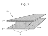
- Fig. 7 shows the structure of a general NRD guide 10.
- the conventional and general NRD guide 10 has the structure in which two conductive plates 1 and 2 approximately parallel to each other sandwich a dielectric strip 4 having a width smaller than that of the conductive plates 1 and 2. Parts 3 between the two conductive plates 1 and 2 other than the dielectric strip 4 are voids (air).
- the width of the dielectric strip 4 is smaller than the width of the conductive plates 1 and 2, and the contact area therebetween is small, when the NRD guide 10 is handled, it is difficult to ensure the strength to retain the structure described above.
- Techniques for ensuring the strength of the NRD guide 10 have been disclosed in Japanese Unexamined Patent Application Publication Nos. 3-270401, 6-45807, and 8-65015.
- the present invention was made in consideration of the situations described above, and an object of the present invention is to provide a dielectric line and a production method therefor, the dielectric line capable of ensuring a sufficient strength and being suitable for mass production.
- the present invention provides a dielectric line which has a dielectric strip provided between two conductive plates approximately parallel to each other and having a width smaller than that of the conductive plates.
- the dielectric strip is composed of a porous material, and the other parts between the two conductive plates other than the dielectric strip are filled with dielectric medium layers composed of a porous material having a dielectric constant smaller than that of the dielectric strip.
- the dielectric constant of the dielectric strip is preferably 1.5 times or more the dielectric constant of the dielectric medium layer.
- the dielectric strip and the dielectric medium layers are filled between the two conductive plates, compared to a conventional dielectric line (see Fig. 7) in which the parts other than the dielectric strip are voids (air), the dielectric strip is unlikely to be displaced, and as a result, the strength is significantly increased, thereby forming a stable structure.
- the porous materials are used for the dielectric strip and the dielectric medium layers, by increasing the porosity thereof, the dielectric constant and the dielectric loss can be significantly decreased, and as a result, high frequency signals can be transmitted with very high transmission efficiency (low loss).
- the case may also be considered in which the dielectric strip and the dielectric medium layers are formed of a substantially identical material and have different porosities from each other.
- an NRD guide nonradiative dielectric line
- the difference in dielectric constant between the dielectric strip and the dielectric medium layer is important.
- the dielectric constant has a predetermined value which is determined by the material thereof; hence, when the difference in dielectric constant is to be adjusted, a plurality of dielectric materials must be used.
- the dielectric constant thereof depends on the porosity (the higher the porosity, the lower the dielectric constant); hence, by adjusting the porosity, the dielectric strip and the dielectric medium layers can be formed.
- the term “identical” substantially means that primary materials are identical with each other, and slight difference in component caused by different production conditions (drying condition and the like) is also included substantially in the scope of the “identical” (hereinafter, the above term is to be construed as described above).
- the dielectric constant is adjusted by changing the porosity
- the dielectric strip and the dielectric medium layers can be formed from one type of material, and hence the production can be easily performed (reduction in production cost).
- the mass production can be suitably performed, and complicated shapes can also be produced.
- an optional dielectric constant can be realized.
- dielectric strips having optional dielectric constants can be formed on one substrate (conductive plate)
- an NRD guide capable of responding to transmission signals having different frequencies can be formed on one substrate.
- a plurality of dielectric materials which have different dielectric constants from each other is necessarily disposed, and in some cases, since a dielectric material having a desired dielectric constant was not present, an NRD guide responding to the frequency of a specific transmission signal could not be formed.
- the degree of freedom of designing the NRD guide is significantly increased.
- an aerogel material may be mentioned.
- the present invention also provides a method for producing the dielectric line described above.
- the method is a method for producing a dielectric line having a dielectric strip provided between two conductive plates approximately parallel to each other and having a width smaller than that of the conductive plates, and dielectric medium layers filled between the conductive plates other than the dielectric strip and composed of a porous material having a dielectric constant smaller than that of the dielectric strip.
- the method described above has a film forming step of forming a film on one of the conductive plates using a dielectric raw material, a strip exposure step of exposing a part of the film of the dielectric raw material to predetermined light, beams, and vapor, the part having a shape corresponding to the dielectric strip, and a pore forming step of making the entire film of the dielectric raw material porous.
- the other parts which are not processed by the exposure process that is, the parts corresponding to the dielectric medium layers
- the dielectric strip and the dielectric medium layers can be formed so as to have well-balanced dielectric constants, that is what required as the dielectric line.
- the chemical reaction caused by the heat treatment is moderate as compared to that by the strip exposure step, and hence the difference in density also occurs between the part having a shape corresponding to the dielectric strip and the other parts.
- a step may be mentioned in which the part having a shape corresponding to the dielectric strip is exposed to ultraviolet rays, electron beams, X-rays, or ion beams, and in this case, the dielectric raw material may contain a photosensitive material.
- the strip exposure step a step may be mentioned in which the part having a shape corresponding to the dielectric strip is exposed to moisture vapor, vapor containing an acidic material, vapor containing a basic material, or vapor containing a dielectric raw material.
- the substantially identical material is used for the dielectric strip and the dielectric medium layers; however, the present invention is not limited thereto, and different materials may also be used in some cases.
- the method described above has a first film forming step of forming a first film on one of the conductive plates using a first dielectric raw material, a film removing step of removing the first film except for a part having a shape corresponding to the dielectric strip, a second film forming step of forming a second film using a second dielectric raw material on said one of the two conductive plates which is processed by the film removing step, and a pore forming step of making porous the entire films of the first and the second dielectric raw materials.
- the parts corresponding to the dielectric medium layers are formed by the second film of the second dielectric raw material in the second film forming step.
- the dielectric line can also be formed.
- the film removing step for example, there may be mentioned a step in which, in the first film of the first dielectric raw material, after the part having a shape corresponding to the dielectric strip is exposed to predetermined light or beams, followed by development treatment, the other parts other that the part having a shape corresponding to the dielectric strip are removed.
- the film formed in the above film forming step chemical bonds are not substantially formed before the strip exposure step is performed, and the film is in an incomplete state. That is, since having a low molecular weight, the film is soluble in various solvents (organic solvents and alkaline solvents). Accordingly, after the part having a shape corresponding to the dielectric strip is exposed to the light or beams described above so as to facilitate the formation of chemical bonds, the parts other than the part (part exposed to the light or beams) having a shape corresponding to the dielectric strip can be selectively removed by development treatment.
- the first dielectric raw material contains a photosensitive material
- light or beams having sufficient energy may be used in order to facilitate the chemical reaction (polymerization reaction) of molecules in the film; however, when the photosensitive material is used as described above, the exposure amount of light or beams can be reduced, and as a result, various advantages, such as decrease in time for treatment and easy treatment using a simple device, can be obtained.
- photosensitive material for example, a photo-acid generator may be mentioned.
- a raw material containing an organic metal material may be mentioned.
- organic metal material a metal alkoxide may be mentioned by way of example.
- a raw material containing a surfactant may also be mentioned.
- a step of exposing the dielectric raw material to a supercritical fluid may be mentioned.
- the pore forming step for example, a step of exposing the film to an alcohol-based organic solvent having a high polarity may be mentioned; however, by the step of exposing the film to the supercritical fluid having a low surface tension, the supercritical fluid can be diffused into very fine areas, and as a result, the surfactant even in very fine areas can be effectively removed.
- the supercritical fluid for example, carbon dioxide, ethanol, methanol, water, ammonia, and a fluorinated carbon material may be used alone or in combination.
- the pore forming step includes a step of performing heat treatment following the step of exposing the dielectric raw material to a supercritical fluid, the film quality can be stabilized.
- the heat treatment in the pore forming step may be performed at 200°C or more.
- the film is formed of a silica material (one example of a dielectric raw material), Si-O bonds are enhanced.
- Fig. 1 is a perspective view showing the structure of a dielectric line X of an embodiment according to the present invention.
- Fig. 2 is a graph showing the relationship between the porosity and the relative dielectric constant of a porous material.
- Fig. 3 is a flowchart showing the procedure of a production method of the dielectric line X of an embodiment according to the present invention.
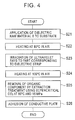
- Fig. 4 is a flowchart showing the procedure of a production method of the dielectric line X of a first example according to the present invention.
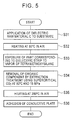
- Fig. 5 is a flowchart showing the procedure of a production method of the dielectric line X of a second example according to the present invention.
- Fig. 6 is a flowchart showing the procedure of a production method of the dielectric line X of a third example according to the present invention.
- Fig. 7 is a perspective view showing the structure of a conventional general NRD guide.
- Fig. 1 is a perspective view showing the structure of a dielectric line X of an embodiment according to the present invention
- Fig. 2 is a graph showing the relationship between the porosity and the relative dielectric constant of a porous material
- Fig. 3 is a flowchart showing the procedure of a production method of the dielectric line X of an embodiment according to the present invention
- Fig. 4 is a flowchart showing the procedure of a production method of the dielectric line X of a first example according to the present invention
- Fig. 5 is a flowchart showing the procedure of a production method of the dielectric line X of a second example according to the present invention
- Fig. 6 is a flowchart showing the procedure of a production method of the dielectric line X of a third example according to the present invention
- Fig. 7 is a perspective view showing the structure of a conventional general NRD guide.
- the dielectric line X has the structure composed of two conductive plates 1 and 2 and a dielectric strip 40 which is provided therebetween and which has a width smaller than that of the conductive plates 1 and 2, and the structure described above is the same as that of the conventional dielectric line (NRD guide) shown in Fig. 7; however, the points different therefrom are as follows. That is, the dielectric strip 40 is formed of a porous material, and parts which are between the conductive plates 1 and 2 other than the dielectric strip 40 are filled with dielectric medium layers 30 composed of a porous material having a dielectric constant smaller than that of the dielectric strip 40.
- the dielectric strip 40 and the dielectric medium layers 30 are filled between the two conductive plates 1 and 2 as described above, compared to the dielectric line which has been primarily used (shown in Fig. 7, in which the parts other than the dielectric strip are voids (air)), the displacement of the dielectric strip 40 is unlikely to occur, and the strength is significantly enhanced to form a stable structure.
- the porous materials are used for the dielectric strip 40 and the dielectric medium layers 30, by increasing the porosity thereof, the dielectric constant and the dielectric loss can be considerably decreased, and as a result, high frequency signals can be transmitted with very high transmission efficiency (low loss). Furthermore, by optionally selecting the porosity of the porous material, a desired dielectric constant can be realized (see Fig. 2), and hence the degree of freedom of designing is significantly increased.
- Fig. 2 is a graph showing the relationship between the porosity and the dielectric constant of a dielectric film formed of a metal alkoxide (tetramethoxysilane) as a raw material, the dielectric film being one example of a porous material.
- the porosity is increased, the relative dielectric constant linearly approaches 1.00. That is, when the porosity of the porous material is infinitely increased to 100%, properties (relative dielectric constant and dielectric loss) can be obtained which are infinitely close to the properties of air.
- the distance between the two conductive plates 1 and 2 (that is, the thickness of the dielectric strip 40 and that of the dielectric medium layers 30) is formed to be one-half or less the wavelength of a signal in the dielectric medium layer 30, the signal being transmitted through this dielectric line X.
- the dielectric line X forms an NRD guide (nonradiative dielectric line) in which unnecessary radiation of transmission signals does not occur. Accordingly, efficient signal transmission having no radiation loss can be performed.
- S11, S12, ⁇ each indicate the ordinal number of a process step (step).
- a dielectric raw material A which is a predetermined dielectric raw material, is applied to a substrate which is the conductive plate 1, one of the two conductive plates described above, so as to have a predetermined thickness (S11). This thickness is one-half or less the wavelength of a signal in the dielectric medium layer 30, the signal being transmitted through the dielectric line X.
- the dielectric raw material A is a solution prepared by the following procedure. That is, after 2 g of tetramethoxysilane (metal alkoxide) Si(CH 3 O) 4 , which is one example of an organic metal compound), 10 g of ethanol, 2 g of butanol, 1 g of methyl 3-methoxypropionate, and 1.2 g of water at a pH of 3 are mixed and stirred, the mixture thus prepared is held at 60°C for approximately 6 hours for facilitating reaction thereof to form a solution, a transparent solution is then prepared by mixing the above solution with IBCF (manufactured by Sanwa Chemical Co., Ltd.), which is a photo-acid generator, at a ratio of 0.05% (percent by weight), and subsequently, 0.2 g of hexadecyltrimethylammonium chloride (one example of a surfactant) is mixed with 10 cc of the above solution, followed by stirring.
- IBCF manufactured by Sanwa Chemical Co
- a part coated with the dielectric raw material A described above is dried by heating (baking) at 80°C in the air, so that the film of the dielectric raw material A is formed (S12).
- This heating is performed for a sufficient period of time (such as approximately 1 to 5 minutes) to remove an excess solvent (necessary for coating but unnecessary thereafter) such as ethanol contained in the raw material solution and to stabilize the film on the substrate by increasing the viscosity of the film.
- S11 and S12 are one example of the film forming step.
- the film of the above dielectric raw material A which has a shape corresponds to the dielectric strip 40, is irradiated with electron beams (that is, the part having a shape corresponding to the dielectric strip 40 is exposed to electron beams) (S13).
- electron beams for example, electron beams at an acceleration voltage of 50 keV and a dose of 10 ⁇ C/cm 2 are used.
- Si-OH bonds formed from tetramethoxysilane are formed into Si-O bonds (a so-called crosslinking reaction).
- the film formed before the irradiation of electron beams has not an ideal silica structure and still has many unreacted portions (in particular, Si-OH bonds).
- the unreacted portions thereof are cross-linked, and as a result, the bones as the silica can be progressively strengthened.
- micelle structures formed by the surfactant are destroyed. That is, since the micelle structures are destroyed, and the crosslinking reaction progresses, a higher dense structure can be formed.
- heating is performed for the film of the dielectric raw material A at 100°C in the air (S14).
- This step is a step of facilitating a crosslinking reaction of the parts which are not irradiated with electron beams and is performed, for example, for approximately 1 to 5 minutes.
- the temperature and/or the pressure is increased, so that the CO 2 is placed in a supercritical state.
- a fluid in a supercritical state may be charged into a pressure container in which the dielectric material is placed.
- the dielectric raw material processed by the extraction treatment described above is heated to 200°C in the air (S16). This heating is performed, for example, for approximately 5 to 30 minutes.
- S15 and S16 are one example of the above pore forming step.
- the layer of the dielectric raw material A since parts at which the organic component was previously present and was already removed are formed into pores, a layer made of a porous material is formed on the substrate (that is, one of the two conductive plates, the conductive plate 1).
- the other parts that is, the parts corresponding to the dielectric medium layers 30
- the relative dielectric constant of the part irradiated with electron beams (that is, the part corresponding to the dielectric strip 40) was 2.0, and the relative dielectric constant of the other parts (that is, the parts corresponding to the dielectric medium layers 30) was 1.5.
- the dielectric strip 40 and the dielectric medium layers 30 are formed so as to have well-balanced dielectric constants, that is what required as the dielectric line.
- the dielectric strip 40 and the dielectric medium layers 30 formed in this embodiment are aerogel materials (dry aerogel materials) having different porosities.
- the other conductive plate 2 is adhered (S17), and hence the dielectric line X can be formed.
- Step 13 instead of the irradiation of electron beams described above, when irradiation of X-rays (for example, having an electron energy of 1 GeV) or irradiation of ion beams (such as Be 2+ irradiation at an energy of 200 keV and at an ion dose of 1e 13 to 1e 14 /cm 2 ) is performed, a similar result can also be obtained.
- irradiation of X-rays for example, having an electron energy of 1 GeV
- irradiation of ion beams such as Be 2+ irradiation at an energy of 200 keV and at an ion dose of 1e 13 to 1e 14 /cm 2
- a mixture containing two or more materials may be used, in which at least one of the above two or more materials may be selected from the group consisting of carbon dioxide, ethanol, methanol, water, ammonia, and a fluorinated carbon material.
- a solvent may also be added in order to improve the performance of the extraction treatment.
- a solvent to be used in this case in view of compatibility with CO 2 , an organic solvent is preferably used.
- organic solvents for example, alcohol-based solvents, ketone-based solvents, and amide-based solvents may be mentioned.
- alcohol-based solvents for example, methanol, ethanol, n-propanol, isopropanol, n-butanol, isobutanol, sec-butanol, t-butanol, n-pentanol, isopentanol, 2-methylbutanol, sec-pentanol, t-pentanol, 3-methoxybutanol, n-hexanol, 2-methylpentanol, sec-hexanol, and 2-ethylbutanol may be mentioned.
- ketone-based solvents for example, acetone, methyl ethyl ketone, methyl n-propyl ketone, methyl n-butyl ketone, diethyl ketone, methyl i-butyl ketone, methyl n-pentyl ketone, ethyl n-butyl ketone, methyl n-hexyl ketone, and di-n-butyl ketone may be mentioned.
- amide-based solvents for example, formamide, N-methylformamide, N,N'-dimethylformamide, N-ethylformamide, N,N'-diethylformamide, acetoamide, N-methylacetoamide, N,N'-dimethylacetoamide, N-ethylacetoamide, N,N'-diethylacetoamide, N-methylpropionamide, and N-methyl pyrrolidone may be mentioned.
- nonionic surfactants generally known materials such as nonionic surfactants and cationic surfactants may be used.
- nonionic surfactants for example, ethylene oxide derivatives and propylene oxide derivatives may be used.
- quaternary ammonium salts of an alkyl group having 8 to 24 carbon atoms such as C n H 2n+1 (CH 3 ) 3 N+X-, C n H 2n+1 (C 2 H 5 ) 3 N+X- (X indicates an element to be turned into a negative ion), C n H 2n+1 NH 2 , and H 2 N(CH 2 ) n NH 2 may be mentioned.
- X indicates an anion (in particular, Cl - , Br - , or the like)
- M indicates a hydrogen atom or a lower alkyl group (in particular, CH 3 , C 2 H 5 , or the like).
- the surfactants mentioned above may be used alone or in combination.
- an inorganic material is superior in terms of heat stability, processability, and mechanical strength.
- oxides of titanium, silicon, aluminum, boron, germanium, lanthanum, magnesium, niobium, phosphorous, tantalum, tin, vanadium, and zirconium may be mentioned.
- metal alkoxides of the above metals are used as the raw materials, in the film forming step, the mixing with the surfactants can be preferably performed.
- metal alkoxides for example, there may be mentioned tetraethoxytitanium, tetraisopropoxytitanium, tetramethoxytitanium, tetra-n-butoxytitanium, tetraethoxysilane, tetraisopropoxysilane, tetramethoxysilane, tetra-n-butoxysilane, triethoxyfluorosilane, triethoxysilane, triisopropoxyfluorosilane, trimethoxyfluorosilane, tirmethoxysilane, tri-n-butoxyfluorosilane, tri-n-propoxyfluorosilane, trimethylmethoxysilane, trimethylethoxysilane, trimethychlorosilane, phenyltriethoxysilane, phenyldiethoxychlorosilane, methyltrimethoxysilane, methyltriethoxy
- tetraisopropoxytitanium, tetra-n-butoxytitanium, tetraethoxysilane, tetraisopropoxysilane, tetramethoxysilane, tetra-n-butoxysilane, triisobutoxyaluminum, and trisisopropoxyaluminum may be mentioned as preferable materials by way of example.
- Those metal alkoxides may be used alone or in combination.
- the inorganic materials a material primarily composed of silica is preferably used since a layer having a low dielectric constant can be obtained.
- a dielectric raw material B which was a predetermined dielectric raw material, was applied to a substrate which was the conductive plate 1, one of the two conductive plates described above, so as to have a predetermined thickness (S21).
- the dielectric raw material B was prepared by the following procedure. After 2 g of tetramethoxysilane (metal alkoxide) Si(CH 3 O) 4 , which was one example of an organic metal material, 10 g of ethanol, 2 g of butanol, 1 g of methyl 3-methoxypropionate, and 1.2 g of water at a pH of 3 were mixed and stirred, the mixture thus prepared was held at 60°C for approximately 6 hours for facilitating reaction thereof to form a solution, a transparent solution was then prepared by mixing the above solution with IBCF (manufactured by Sanwa Chemical Co., Ltd.), which was a photo-acid generator, at a ratio of 0.05% (percent by weight), and subsequently, 0.2 g of hexadecyltrimethylammonium chloride (one example of a surfactant) was mixed whit 10 cc of the above transparent solution, followed by stirring. Next, the solution thus prepared was processed by heating (baking) at
- a part coated with the dielectric raw material B described above was dried by heating (baking) at 80°C in the air, so that the film of the dielectric raw material B was formed (S22).
- This heating was performed for a sufficient period of time (such as approximately 1 to 5 minutes) to stabilize the film on the substrate by increasing the viscosity of the film.
- S21 and S22 are one example of the film forming step.
- Si-O bonds were formed by a crosslinking reaction.
- heating was performed for the film of the dielectric raw material B at 100°C in the air (S24).
- This step was a step of also facilitating a crosslinking reaction of parts which were not irradiated with ultraviolet rays and was performed, for example, for approximately 1 to 5 minutes.
- the other conductive plate 2 was adhered (S26), so that the dielectric line X could be formed.
- the other parts that is, the parts corresponding to the dielectric medium layers 30
- the relative dielectric constants of the layers of the porous materials formed by the steps described above were measured, the relative dielectric constant of the part corresponding to the dielectric strip 40 was 2.0, and the relative dielectric constant of the other parts (that is, the parts corresponding to the dielectric medium layers 30) was 1.5.
- a dielectric raw material C which was a predetermined dielectric raw material, was applied to a substrate which was one of the two conductor plates described above, the conductive plate 1, so as to have a predetermined thickness (S31).
- the dielectric raw material C was a solution prepared by the following procedure. After 2 g of tetramethoxysilane (metal alkoxide) Si(CH 3 O) 4 , which was one example of an organic metal material, 10 g of ethanol, 2 g of butanol, 1 g of methyl 3-methoxypropionate, and 1.2 g of water at a pH of 3 were mixed and stirred, the mixture thus prepared was held at 60°C for approximately 6 hours for facilitating reaction thereof so as to prepare a transparent solution, and 10 cc of this solution was mixed with 0.2 g of hexadecyltrimethylammonium chloride (one example of a surfactant), followed by stirring.
- tetramethoxysilane (metal alkoxide) Si(CH 3 O) 4 which was one example of an organic metal material
- a part coated with the dielectric raw material C described above was dried by heating (baking) at 80°C in the air, so that the film of the dielectric raw material C was formed (S32).
- This heating was performed for a sufficient period of time (such as approximately 1 to 5 minutes) to stabilize the film on the substrate by increasing the viscosity of the film.
- S31 and S32 are one example of the film forming step.
- Si-O bonds were formed by a crosslinking reaction.
- Steps 34 and 35 are one example of the pore forming step.
- the other conductive plate 2 was adhered (S36), so that the dielectric line X could be formed.
- the other parts that is, the parts corresponding to the dielectric medium layers 30
- the relative dielectric constants of the layers of the porous materials formed by the steps described above were measured, the relative dielectric constant of the part corresponding to the dielectric strip 40 was 2.0, and the relative dielectric constant of the other parts (that is, the parts corresponding to the dielectric medium layers 30) was 1.5.
- Step 33 instead of the exposure to vapor of tetraethoxysilane, for example, by exposure to vapor of silicon alkoxide such as tetramethoxysilane, exposure to moisture vapor (such as moisture vapor at 100°C and 1 atmospheric pressure), exposure to vapor of another acidic material (such as vapor of a saturated aqueous hydrochloric acid solution at 23°C and 1 atmospheric pressure), exposure to vapor of a basic material (such as vapor of a saturated aqueous ammonium solution at 23°C and 1 atmospheric pressure), a result similar to that described above can be obtained.
- moisture vapor such as moisture vapor at 100°C and 1 atmospheric pressure
- another acidic material such as vapor of a saturated aqueous hydrochloric acid solution at 23°C and 1 atmospheric pressure
- a basic material such as vapor of a saturated aqueous ammonium solution at 23°C and 1 atmospheric pressure
- a dielectric raw material E which was a predetermined dielectric raw material, was applied to a substrate which was one of the two conductive plates, the conductor plate 1, so as to have a predetermined thickness (S41).
- S41 and S42 are one example of the first film forming step.
- Si-O bonds were formed by a crosslinking reaction.
- a dielectric raw material F which was a predetermined dielectric raw material, was applied onto the parts of the substrate so as to have a predetermined thickness (S45), the parts being areas at which the film on the substrate was removed.
- heating was performed for the film of the dielectric raw material F at 100°C in the air (S46).
- This step was a step of facilitating a crosslinking reaction of the dielectric raw material F and was performed, for example, for approximately 1 to 5 minutes.
- the other conductive plate 2 was adhered (S49), so that the dielectric line X could be formed.
- film portions that is, the parts corresponding to the dielectric medium layers 30
- the dielectric raw material F also had a high porosity.
- the relative dielectric constants of the layers of the porous materials formed by the steps described above were measured, the relative dielectric constant of the part corresponding to the dielectric strip 40 was 2.0, and the relative dielectric constant of the other parts (that is, the parts corresponding to the dielectric medium layers 30) was 1.5.
- a dielectric line was formed by the same method and conditions as described above.
- the parts corresponding to the dielectric medium layers 30 had a relative dielectric constant of 1.8.
- the relative dielectric constant of the parts corresponding to the dielectric medium layers 30 can be adjusted to an optional value.
- a dielectric line was formed by the same method and conditions as described above.
- the parts corresponding to the dielectric medium layers 30 had a relative dielectric constant of 1.8.
- the dielectric constant of the parts corresponding to the dielectric medium layers 30 can be changed.
- the dielectric strip since the space between the two conductive plates is filled with the dielectric strip and the dielectric medium layers, compare to the conventional dielectric line in which parts other than the dielectric strip are composed of voids (air), the dielectric strip is not likely to be displaced, and the strength is significantly improved to form a stable structure.
- the porous materials are used for the dielectric strip and the dielectric medium layers, by increasing the porosity thereof, the dielectric constant and the dielectric loss can be significantly decreased. As a result, high frequency signals can be transmitted with very high transmission efficiency (low loss).
- the dielectric strip and the dielectric medium layers can be formed from one type of material, and hence the production can be easily performed (reduction in production cost).
- the production can be performed using a patterning process, compared to the conventional case in which a three-dimensional structure is produced by machining, the mass production can be suitably performed, and complicated shapes can also be easily produced.
- a plurality of dielectric strips having optional dielectric constants can be formed on one substrate (conductive plate), and hence an NRD guide capable of responding transmission signals having different frequencies can be formed on one substrate. As a result, the degree of freedom of designing an NRD guide is significantly increased.
Landscapes
- Engineering & Computer Science (AREA)
- Manufacturing & Machinery (AREA)
- Laminated Bodies (AREA)
- Waveguides (AREA)
- Internal Circuitry In Semiconductor Integrated Circuit Devices (AREA)
Abstract
Description
Claims (18)
- A dielectric line comprising: a dielectric strip provided between two conductive plates approximately parallel to each other and having a width smaller than that of the conductive plates,
wherein the dielectric strip is composed of a porous material, and
the other parts between the two conductive plates other than the dielectric strip are filled with dielectric medium layers composed of a porous material having a dielectric constant smaller than that of the dielectric strip. - The dielectric line according to Claim 1, wherein the dielectric strip and the dielectric medium layers are composed of a substantially identical material and have different porosities from each other.
- The dielectric line according to Claim 1, wherein the distance between the two conductive plates is one-half or less the wavelength of a signal in the dielectric medium layers, the signal being transmitted through the dielectric line.
- The dielectric line according to Claim 1, wherein the dielectric strip and the dielectric medium layers are composed of an aerogel material.
- A method for producing a dielectric line having a dielectric strip provided between two conductive plates approximately parallel to each other and having a width smaller than that of the conductive plates, and dielectric medium layers filled between the conductive plates other than the dielectric strip and composed of a porous material having a dielectric constant smaller than that of the dielectric strip, the method comprising:a film forming step of forming a film on one of the conductive plates using a dielectric raw material;a strip exposure step of exposing a part of the film of the dielectric raw material to predetermined light, beams, or vapor, the part having a shape corresponding to the dielectric strip; anda pore forming step of making the entire film of the dielectric raw material porous.
- The method for producing a dielectric line, according to Claim 5,
wherein the strip exposure step is a step of exposing the part having a shape corresponding to the dielectric strip to ultraviolet rays, electron beams, X-rays, or ion beams, and
the dielectric raw material comprises a photosensitive material. - The method for producing a dielectric line, according to Claim 5,
wherein the strip exposure step is a step of exposing the part having a shape corresponding to the dielectric strip to moisture vapor, vapor containing an acidic material, vapor containing a basic material, or vapor containing a dielectric raw material. - The method for producing a dielectric line, according to Claim 6, wherein the photosensitive material comprises a photo-acid generator.
- The method for producing a dielectric line, according to Claim 5, wherein the dielectric raw material comprises an organic metal material.
- The method for producing a dielectric line, according to Claim 9, wherein the organic metal material comprises a metal alkoxide.
- The method for producing a dielectric line, according to Claim 5, wherein the dielectric raw material comprises a surfactant.
- A method for producing a dielectric line having a dielectric strip provided between two conductive plates approximately parallel to each other and having a width smaller than that of the conductive plates, and dielectric medium layers filled between the conductive plates other than the dielectric strip and composed of a porous material having a dielectric constant smaller than that of the dielectric strip, the method comprising:a first film forming step of forming a first film using a first dielectric raw material on one of the conductive plates;a film removing step of removing the first film except for a part having a shape corresponding to the dielectric strip;a second film forming step of forming a second film using a second dielectric raw material on said one of the two conductive plates which is processed by the film removing step; anda pore forming step of making porous the entire films of the first dielectric raw material and the second dielectric raw material.
- The method for producing a dielectric line, according to Claim 12, wherein the film removing step comprises exposing the part of the first film of the first dielectric raw material to predetermined light or beams, the part having a shape corresponding to the dielectric strip, and then performing development treatment to remove the first film other than the part having a shape corresponding to the dielectric strip.
- The method for producing a dielectric line, according to Claim 12, wherein the first dielectric raw material comprises a photosensitive material.
- The method for producing a dielectric line, according to Claim 14, wherein the photosensitive material comprises a photo-acid generator.
- The method for producing a dielectric line, according to Claim 12, wherein the dielectric raw material comprises an organic metal material.
- The method for producing a dielectric line, according to Claim 16, wherein the organic metal material comprises a metal alkoxide.
- The method for producing a dielectric line, according to Claim 12, wherein the dielectric raw material comprises a surfactant.
Applications Claiming Priority (3)
| Application Number | Priority Date | Filing Date | Title |
|---|---|---|---|
| JP2003019344 | 2003-01-28 | ||
| JP2003019344A JP3886459B2 (en) | 2003-01-28 | 2003-01-28 | Dielectric line manufacturing method |
| PCT/JP2004/000012 WO2004068628A1 (en) | 2003-01-28 | 2004-01-05 | Dielectric line and production method therefor |
Publications (3)
| Publication Number | Publication Date |
|---|---|
| EP1589605A1 true EP1589605A1 (en) | 2005-10-26 |
| EP1589605A4 EP1589605A4 (en) | 2006-08-02 |
| EP1589605B1 EP1589605B1 (en) | 2009-10-21 |
Family
ID=32820607
Family Applications (1)
| Application Number | Title | Priority Date | Filing Date |
|---|---|---|---|
| EP04700170A Expired - Lifetime EP1589605B1 (en) | 2003-01-28 | 2004-01-05 | Dielectric line and production method therefor |
Country Status (7)
| Country | Link |
|---|---|
| US (2) | US7432038B2 (en) |
| EP (1) | EP1589605B1 (en) |
| JP (1) | JP3886459B2 (en) |
| KR (1) | KR100699655B1 (en) |
| CN (1) | CN1331271C (en) |
| DE (1) | DE602004023689D1 (en) |
| WO (1) | WO2004068628A1 (en) |
Cited By (1)
| Publication number | Priority date | Publication date | Assignee | Title |
|---|---|---|---|---|
| EP3518280A1 (en) * | 2018-01-25 | 2019-07-31 | Murata Manufacturing Co., Ltd. | Electronic products having embedded porous dielectric, related semiconductor products, and their methods of manufacture |
Families Citing this family (14)
| Publication number | Priority date | Publication date | Assignee | Title |
|---|---|---|---|---|
| US7696625B2 (en) * | 2004-11-30 | 2010-04-13 | Semiconductor Energy Laboratory Co., Ltd. | Semiconductor device and method for manufacturing the same |
| US7732349B2 (en) * | 2004-11-30 | 2010-06-08 | Semiconductor Energy Laboratory Co., Ltd. | Manufacturing method of insulating film and semiconductor device |
| US7985677B2 (en) * | 2004-11-30 | 2011-07-26 | Semiconductor Energy Laboratory Co., Ltd. | Method of manufacturing semiconductor device |
| JP4887342B2 (en) * | 2008-10-06 | 2012-02-29 | 株式会社日立製作所 | Dielectric waveguide and manufacturing method thereof |
| FR2980040B1 (en) * | 2011-09-14 | 2016-02-05 | Commissariat Energie Atomique | ORGANIC FIELD EFFECT TRANSISTOR |
| JP5787108B2 (en) * | 2013-08-02 | 2015-09-30 | Tdk株式会社 | Dielectric lines and electronic components |
| JP6183624B2 (en) * | 2015-04-24 | 2017-08-23 | Tdk株式会社 | Electronic components |
| KR101874694B1 (en) * | 2016-03-28 | 2018-07-04 | 한국과학기술원 | Waveguide for transmission of electomagnetic signal |
| US11165129B2 (en) * | 2016-12-30 | 2021-11-02 | Intel Corporation | Dispersion reduced dielectric waveguide comprising dielectric materials having respective dispersion responses |
| DE112017007891T5 (en) * | 2017-09-29 | 2020-05-07 | Intel Corporation | INTRA-SEMICONDUCTOR-THE-COMMUNICATION VIA WAVEGUIDES IN A MULTI-DIE-SEMICONDUCTOR HOUSING |
| JP6948904B2 (en) * | 2017-09-29 | 2021-10-13 | 株式会社Soken | Spark plug for internal combustion engine |
| TWI715962B (en) * | 2018-04-06 | 2021-01-11 | 韓國科學技術院 | Waveguide for transmission of electromagnetic wave signals |
| US11329359B2 (en) | 2018-05-18 | 2022-05-10 | Intel Corporation | Dielectric waveguide including a dielectric material with cavities therein surrounded by a conductive coating forming a wall for the cavities |
| CN114464970A (en) * | 2022-02-10 | 2022-05-10 | 南京信息工程大学 | A terahertz bandstop filter based on sagnac loop |
Family Cites Families (21)
| Publication number | Priority date | Publication date | Assignee | Title |
|---|---|---|---|---|
| GB2085660A (en) * | 1980-10-16 | 1982-04-28 | Marconi Co Ltd | Waveguides |
| JPS57166701A (en) * | 1981-04-03 | 1982-10-14 | Shigeo Nishida | Dielectric line |
| JPS58215804A (en) * | 1982-06-09 | 1983-12-15 | Seki Shoji Kk | Dielectric line |
| JPS6451202A (en) | 1987-08-20 | 1989-02-27 | Sumitomo Electric Industries | Cutting tool covered with diamond |
| JPH0254602A (en) * | 1988-08-19 | 1990-02-23 | Junkosha Co Ltd | High frequency transmission circuit |
| JP2692328B2 (en) | 1990-03-20 | 1997-12-17 | 株式会社村田製作所 | NRD guide |
| JP3125164B2 (en) | 1992-07-24 | 2001-01-15 | 本田技研工業株式会社 | Non-radiative dielectric line |
| JP3123293B2 (en) | 1993-03-05 | 2001-01-09 | 株式会社村田製作所 | Non-radiative dielectric line and method of manufacturing the same |
| JPH0865015A (en) | 1994-08-25 | 1996-03-08 | Honda Motor Co Ltd | NRD guide and NRD guide circuit element |
| JPH08228105A (en) * | 1995-02-21 | 1996-09-03 | Sumitomo Electric Ind Ltd | Microstrip substrate |
| US5736425A (en) * | 1995-11-16 | 1998-04-07 | Texas Instruments Incorporated | Glycol-based method for forming a thin-film nanoporous dielectric |
| JP3377932B2 (en) * | 1997-06-30 | 2003-02-17 | 京セラ株式会社 | Method of manufacturing multilayer wiring board for high frequency |
| JP3356120B2 (en) | 1999-06-24 | 2002-12-09 | 株式会社村田製作所 | Method of manufacturing dielectric line |
| JP2001237617A (en) * | 1999-12-13 | 2001-08-31 | Tdk Corp | Transmission line |
| JP3407710B2 (en) | 2000-04-26 | 2003-05-19 | 株式会社村田製作所 | Method of manufacturing dielectric line |
| JP2002076717A (en) * | 2000-09-05 | 2002-03-15 | Matsushita Electric Ind Co Ltd | Dielectric composite porcelain, high-frequency circuit element and high-frequency circuit component using the same |
| JP2002308678A (en) | 2001-02-08 | 2002-10-23 | Sumitomo Electric Ind Ltd | Porous ceramic and method for producing the same |
| JP2003115705A (en) | 2001-07-31 | 2003-04-18 | Sumitomo Electric Ind Ltd | Microstrip substrate |
| US6800360B2 (en) * | 2001-02-08 | 2004-10-05 | Sumitomo Electric Industries, Ltd. | Porous ceramics and method of preparing the same as well as microstrip substrate |
| JP2003089585A (en) | 2001-09-13 | 2003-03-28 | Sumitomo Electric Ind Ltd | Porous ceramics and method for producing the same |
| TW594416B (en) * | 2001-05-08 | 2004-06-21 | Shipley Co Llc | Photoimageable composition |
-
2003
- 2003-01-28 JP JP2003019344A patent/JP3886459B2/en not_active Expired - Fee Related
-
2004
- 2004-01-05 KR KR1020057013861A patent/KR100699655B1/en not_active Expired - Fee Related
- 2004-01-05 EP EP04700170A patent/EP1589605B1/en not_active Expired - Lifetime
- 2004-01-05 CN CNB2004800030637A patent/CN1331271C/en not_active Expired - Fee Related
- 2004-01-05 DE DE602004023689T patent/DE602004023689D1/en not_active Expired - Lifetime
- 2004-01-05 US US10/543,135 patent/US7432038B2/en not_active Expired - Fee Related
- 2004-01-05 WO PCT/JP2004/000012 patent/WO2004068628A1/en not_active Ceased
-
2008
- 2008-09-03 US US12/230,689 patent/US20090017255A1/en not_active Abandoned
Cited By (4)
| Publication number | Priority date | Publication date | Assignee | Title |
|---|---|---|---|---|
| EP3518280A1 (en) * | 2018-01-25 | 2019-07-31 | Murata Manufacturing Co., Ltd. | Electronic products having embedded porous dielectric, related semiconductor products, and their methods of manufacture |
| WO2019145289A1 (en) * | 2018-01-25 | 2019-08-01 | Murata Manufacturing Co., Ltd. | Electronic products having embedded porous dielectric, related semiconductor products, and their methods of manufacture |
| CN111670495A (en) * | 2018-01-25 | 2020-09-15 | 株式会社村田制作所 | Electronic products with embedded porous dielectrics, related semiconductor products, and methods of making the same |
| CN111670495B (en) * | 2018-01-25 | 2024-10-15 | 株式会社村田制作所 | Electronic products with embedded porous dielectrics, related semiconductor products and methods of manufacturing the same |
Also Published As
| Publication number | Publication date |
|---|---|
| US20090017255A1 (en) | 2009-01-15 |
| EP1589605B1 (en) | 2009-10-21 |
| KR100699655B1 (en) | 2007-03-23 |
| WO2004068628A1 (en) | 2004-08-12 |
| JP2004266327A (en) | 2004-09-24 |
| EP1589605A4 (en) | 2006-08-02 |
| CN1331271C (en) | 2007-08-08 |
| JP3886459B2 (en) | 2007-02-28 |
| CN1745497A (en) | 2006-03-08 |
| DE602004023689D1 (en) | 2009-12-03 |
| US20060102937A1 (en) | 2006-05-18 |
| KR20050097957A (en) | 2005-10-10 |
| US7432038B2 (en) | 2008-10-07 |
Similar Documents
| Publication | Publication Date | Title |
|---|---|---|
| US20090017255A1 (en) | Dielectric line and production method therefor | |
| US11347145B2 (en) | Pre-patterned lithography templates | |
| TWI357622B (en) | ||
| US6818139B1 (en) | Method for forming a micro-pattern on a substrate | |
| US7056840B2 (en) | Direct photo-patterning of nanoporous organosilicates, and method of use | |
| JP3057879B2 (en) | Method for manufacturing semiconductor device | |
| TW201241873A (en) | Methods and apparatus for controlling photoresist line width roughness | |
| EP0090615B1 (en) | Method for forming fine resist patterns | |
| JPS641047B2 (en) | ||
| US5127989A (en) | Method of forming a thin film pattern with a trapezoidal cross section | |
| TWI242914B (en) | Dielectric circuit powering antenna | |
| Lee et al. | Ultrasonic and dip resist development processes for 50 nm device fabrication | |
| Liu et al. | Line edge roughness reduction for EUV self-aligned double patterning by surface modification on spin-on-carbon and tone inversion technique | |
| US11782212B1 (en) | Guided-wave-driven metasurface antennas | |
| Busse et al. | Complex modes in circular chirowaveguides | |
| US5186788A (en) | Fine pattern forming method | |
| KR19990003857A (en) | Photosensitive film formation method | |
| CN118778164B (en) | A method for preparing a sub-wavelength multi-step diffractive optical element | |
| JP3267498B2 (en) | Mask, device manufacturing method and exposure apparatus using the same | |
| JP4244341B2 (en) | Dielectric line feed antenna | |
| CN118280798B (en) | Uniformity adjusting device and method for ion beam etching | |
| JP4076475B2 (en) | Method for manufacturing dielectric line filter | |
| JPS5913342A (en) | Manufacture of semiconductor device | |
| CN119105132A (en) | A design method for terahertz electromagnetic wave transmission structure for highly compact on-chip integration | |
| JPH09148313A (en) | Dry etching process |
Legal Events
| Date | Code | Title | Description |
|---|---|---|---|
| PUAI | Public reference made under article 153(3) epc to a published international application that has entered the european phase |
Free format text: ORIGINAL CODE: 0009012 |
|
| 17P | Request for examination filed |
Effective date: 20050713 |
|
| AK | Designated contracting states |
Kind code of ref document: A1 Designated state(s): AT BE BG CH CY CZ DE DK EE ES FI FR GB GR HU IE IT LI LU MC NL PT RO SE SI SK TR |
|
| AX | Request for extension of the european patent |
Extension state: AL LT LV MK |
|
| DAX | Request for extension of the european patent (deleted) | ||
| RBV | Designated contracting states (corrected) |
Designated state(s): DE FR GB |
|
| A4 | Supplementary search report drawn up and despatched |
Effective date: 20060705 |
|
| 17Q | First examination report despatched |
Effective date: 20070227 |
|
| GRAP | Despatch of communication of intention to grant a patent |
Free format text: ORIGINAL CODE: EPIDOSNIGR1 |
|
| GRAS | Grant fee paid |
Free format text: ORIGINAL CODE: EPIDOSNIGR3 |
|
| GRAA | (expected) grant |
Free format text: ORIGINAL CODE: 0009210 |
|
| AK | Designated contracting states |
Kind code of ref document: B1 Designated state(s): DE FR GB |
|
| REG | Reference to a national code |
Ref country code: GB Ref legal event code: FG4D |
|
| REF | Corresponds to: |
Ref document number: 602004023689 Country of ref document: DE Date of ref document: 20091203 Kind code of ref document: P |
|
| PLBE | No opposition filed within time limit |
Free format text: ORIGINAL CODE: 0009261 |
|
| STAA | Information on the status of an ep patent application or granted ep patent |
Free format text: STATUS: NO OPPOSITION FILED WITHIN TIME LIMIT |
|
| 26N | No opposition filed |
Effective date: 20100722 |
|
| REG | Reference to a national code |
Ref country code: FR Ref legal event code: PLFP Year of fee payment: 13 |
|
| PGFP | Annual fee paid to national office [announced via postgrant information from national office to epo] |
Ref country code: GB Payment date: 20151230 Year of fee payment: 13 |
|
| PGFP | Annual fee paid to national office [announced via postgrant information from national office to epo] |
Ref country code: FR Payment date: 20151208 Year of fee payment: 13 |
|
| PGFP | Annual fee paid to national office [announced via postgrant information from national office to epo] |
Ref country code: DE Payment date: 20151229 Year of fee payment: 13 |
|
| REG | Reference to a national code |
Ref country code: DE Ref legal event code: R119 Ref document number: 602004023689 Country of ref document: DE |
|
| GBPC | Gb: european patent ceased through non-payment of renewal fee |
Effective date: 20170105 |
|
| REG | Reference to a national code |
Ref country code: FR Ref legal event code: ST Effective date: 20170929 |
|
| PG25 | Lapsed in a contracting state [announced via postgrant information from national office to epo] |
Ref country code: FR Free format text: LAPSE BECAUSE OF NON-PAYMENT OF DUE FEES Effective date: 20170131 |
|
| PG25 | Lapsed in a contracting state [announced via postgrant information from national office to epo] |
Ref country code: GB Free format text: LAPSE BECAUSE OF NON-PAYMENT OF DUE FEES Effective date: 20170105 Ref country code: DE Free format text: LAPSE BECAUSE OF NON-PAYMENT OF DUE FEES Effective date: 20170801 |