EP1589360A2 - Curved ridge optical waveguide, optical device, and method of manufacturing optical waveguide - Google Patents
Curved ridge optical waveguide, optical device, and method of manufacturing optical waveguide Download PDFInfo
- Publication number
- EP1589360A2 EP1589360A2 EP05013464A EP05013464A EP1589360A2 EP 1589360 A2 EP1589360 A2 EP 1589360A2 EP 05013464 A EP05013464 A EP 05013464A EP 05013464 A EP05013464 A EP 05013464A EP 1589360 A2 EP1589360 A2 EP 1589360A2
- Authority
- EP
- European Patent Office
- Prior art keywords
- curved
- optical waveguide
- ridge structure
- optical path
- optical
- Prior art date
- Legal status (The legal status is an assumption and is not a legal conclusion. Google has not performed a legal analysis and makes no representation as to the accuracy of the status listed.)
- Granted
Links
Images


Classifications
-
- G—PHYSICS
- G02—OPTICS
- G02F—OPTICAL DEVICES OR ARRANGEMENTS FOR THE CONTROL OF LIGHT BY MODIFICATION OF THE OPTICAL PROPERTIES OF THE MEDIA OF THE ELEMENTS INVOLVED THEREIN; NON-LINEAR OPTICS; FREQUENCY-CHANGING OF LIGHT; OPTICAL LOGIC ELEMENTS; OPTICAL ANALOGUE/DIGITAL CONVERTERS
- G02F1/00—Devices or arrangements for the control of the intensity, colour, phase, polarisation or direction of light arriving from an independent light source, e.g. switching, gating or modulating; Non-linear optics
- G02F1/01—Devices or arrangements for the control of the intensity, colour, phase, polarisation or direction of light arriving from an independent light source, e.g. switching, gating or modulating; Non-linear optics for the control of the intensity, phase, polarisation or colour
- G02F1/21—Devices or arrangements for the control of the intensity, colour, phase, polarisation or direction of light arriving from an independent light source, e.g. switching, gating or modulating; Non-linear optics for the control of the intensity, phase, polarisation or colour by interference
- G02F1/225—Devices or arrangements for the control of the intensity, colour, phase, polarisation or direction of light arriving from an independent light source, e.g. switching, gating or modulating; Non-linear optics for the control of the intensity, phase, polarisation or colour by interference in an optical waveguide structure
- G02F1/2255—Devices or arrangements for the control of the intensity, colour, phase, polarisation or direction of light arriving from an independent light source, e.g. switching, gating or modulating; Non-linear optics for the control of the intensity, phase, polarisation or colour by interference in an optical waveguide structure controlled by a high-frequency electromagnetic component in an electric waveguide structure
-
- G—PHYSICS
- G02—OPTICS
- G02B—OPTICAL ELEMENTS, SYSTEMS OR APPARATUS
- G02B6/00—Light guides; Structural details of arrangements comprising light guides and other optical elements, e.g. couplings
- G02B6/10—Light guides; Structural details of arrangements comprising light guides and other optical elements, e.g. couplings of the optical waveguide type
- G02B6/12—Light guides; Structural details of arrangements comprising light guides and other optical elements, e.g. couplings of the optical waveguide type of the integrated circuit kind
- G02B6/12007—Light guides; Structural details of arrangements comprising light guides and other optical elements, e.g. couplings of the optical waveguide type of the integrated circuit kind forming wavelength selective elements, e.g. multiplexer, demultiplexer
-
- G—PHYSICS
- G02—OPTICS
- G02B—OPTICAL ELEMENTS, SYSTEMS OR APPARATUS
- G02B6/00—Light guides; Structural details of arrangements comprising light guides and other optical elements, e.g. couplings
- G02B6/10—Light guides; Structural details of arrangements comprising light guides and other optical elements, e.g. couplings of the optical waveguide type
- G02B6/12—Light guides; Structural details of arrangements comprising light guides and other optical elements, e.g. couplings of the optical waveguide type of the integrated circuit kind
- G02B6/122—Basic optical elements, e.g. light-guiding paths
- G02B6/1228—Tapered waveguides, e.g. integrated spot-size transformers
-
- G—PHYSICS
- G02—OPTICS
- G02B—OPTICAL ELEMENTS, SYSTEMS OR APPARATUS
- G02B6/00—Light guides; Structural details of arrangements comprising light guides and other optical elements, e.g. couplings
- G02B6/10—Light guides; Structural details of arrangements comprising light guides and other optical elements, e.g. couplings of the optical waveguide type
- G02B6/12—Light guides; Structural details of arrangements comprising light guides and other optical elements, e.g. couplings of the optical waveguide type of the integrated circuit kind
- G02B6/122—Basic optical elements, e.g. light-guiding paths
- G02B6/125—Bends, branchings or intersections
-
- G—PHYSICS
- G02—OPTICS
- G02B—OPTICAL ELEMENTS, SYSTEMS OR APPARATUS
- G02B6/00—Light guides; Structural details of arrangements comprising light guides and other optical elements, e.g. couplings
- G02B6/10—Light guides; Structural details of arrangements comprising light guides and other optical elements, e.g. couplings of the optical waveguide type
- G02B6/12—Light guides; Structural details of arrangements comprising light guides and other optical elements, e.g. couplings of the optical waveguide type of the integrated circuit kind
- G02B6/13—Integrated optical circuits characterised by the manufacturing method
- G02B6/134—Integrated optical circuits characterised by the manufacturing method by substitution by dopant atoms
- G02B6/1342—Integrated optical circuits characterised by the manufacturing method by substitution by dopant atoms using diffusion
-
- G—PHYSICS
- G02—OPTICS
- G02B—OPTICAL ELEMENTS, SYSTEMS OR APPARATUS
- G02B6/00—Light guides; Structural details of arrangements comprising light guides and other optical elements, e.g. couplings
- G02B6/24—Coupling light guides
- G02B6/42—Coupling light guides with opto-electronic elements
- G02B6/4201—Packages, e.g. shape, construction, internal or external details
- G02B6/4204—Packages, e.g. shape, construction, internal or external details the coupling comprising intermediate optical elements, e.g. lenses, holograms
- G02B6/4206—Optical features
-
- G—PHYSICS
- G02—OPTICS
- G02B—OPTICAL ELEMENTS, SYSTEMS OR APPARATUS
- G02B6/00—Light guides; Structural details of arrangements comprising light guides and other optical elements, e.g. couplings
- G02B6/10—Light guides; Structural details of arrangements comprising light guides and other optical elements, e.g. couplings of the optical waveguide type
- G02B6/12—Light guides; Structural details of arrangements comprising light guides and other optical elements, e.g. couplings of the optical waveguide type of the integrated circuit kind
- G02B2006/12083—Constructional arrangements
- G02B2006/12097—Ridge, rib or the like
-
- G—PHYSICS
- G02—OPTICS
- G02B—OPTICAL ELEMENTS, SYSTEMS OR APPARATUS
- G02B6/00—Light guides; Structural details of arrangements comprising light guides and other optical elements, e.g. couplings
- G02B6/10—Light guides; Structural details of arrangements comprising light guides and other optical elements, e.g. couplings of the optical waveguide type
- G02B6/12—Light guides; Structural details of arrangements comprising light guides and other optical elements, e.g. couplings of the optical waveguide type of the integrated circuit kind
- G02B2006/12083—Constructional arrangements
- G02B2006/12119—Bend
-
- G—PHYSICS
- G02—OPTICS
- G02B—OPTICAL ELEMENTS, SYSTEMS OR APPARATUS
- G02B6/00—Light guides; Structural details of arrangements comprising light guides and other optical elements, e.g. couplings
- G02B6/10—Light guides; Structural details of arrangements comprising light guides and other optical elements, e.g. couplings of the optical waveguide type
- G02B6/12—Light guides; Structural details of arrangements comprising light guides and other optical elements, e.g. couplings of the optical waveguide type of the integrated circuit kind
- G02B2006/12133—Functions
- G02B2006/12142—Modulator
-
- G—PHYSICS
- G02—OPTICS
- G02B—OPTICAL ELEMENTS, SYSTEMS OR APPARATUS
- G02B6/00—Light guides; Structural details of arrangements comprising light guides and other optical elements, e.g. couplings
- G02B6/24—Coupling light guides
- G02B6/26—Optical coupling means
- G02B6/32—Optical coupling means having lens focusing means positioned between opposed fibre ends
-
- G—PHYSICS
- G02—OPTICS
- G02B—OPTICAL ELEMENTS, SYSTEMS OR APPARATUS
- G02B6/00—Light guides; Structural details of arrangements comprising light guides and other optical elements, e.g. couplings
- G02B6/24—Coupling light guides
- G02B6/26—Optical coupling means
- G02B6/32—Optical coupling means having lens focusing means positioned between opposed fibre ends
- G02B6/322—Optical coupling means having lens focusing means positioned between opposed fibre ends and having centering means being part of the lens for the self-positioning of the lightguide at the focal point, e.g. holes, wells, indents, nibs
-
- G—PHYSICS
- G02—OPTICS
- G02B—OPTICAL ELEMENTS, SYSTEMS OR APPARATUS
- G02B6/00—Light guides; Structural details of arrangements comprising light guides and other optical elements, e.g. couplings
- G02B6/24—Coupling light guides
- G02B6/42—Coupling light guides with opto-electronic elements
- G02B6/4201—Packages, e.g. shape, construction, internal or external details
- G02B6/4204—Packages, e.g. shape, construction, internal or external details the coupling comprising intermediate optical elements, e.g. lenses, holograms
- G02B6/4214—Packages, e.g. shape, construction, internal or external details the coupling comprising intermediate optical elements, e.g. lenses, holograms the intermediate optical element having redirecting reflective means, e.g. mirrors, prisms for deflecting the radiation from horizontal to down- or upward direction toward a device
-
- G—PHYSICS
- G02—OPTICS
- G02F—OPTICAL DEVICES OR ARRANGEMENTS FOR THE CONTROL OF LIGHT BY MODIFICATION OF THE OPTICAL PROPERTIES OF THE MEDIA OF THE ELEMENTS INVOLVED THEREIN; NON-LINEAR OPTICS; FREQUENCY-CHANGING OF LIGHT; OPTICAL LOGIC ELEMENTS; OPTICAL ANALOGUE/DIGITAL CONVERTERS
- G02F2201/00—Constructional arrangements not provided for in groups G02F1/00 - G02F7/00
- G02F2201/06—Constructional arrangements not provided for in groups G02F1/00 - G02F7/00 integrated waveguide
- G02F2201/063—Constructional arrangements not provided for in groups G02F1/00 - G02F7/00 integrated waveguide ridge; rib; strip loaded
Definitions
- the present invention relates to an optical waveguide that is used for optical communication.
- the present invention relates to an optical waveguide of a diffusion type waveguide capable of reducing a curvature of a curved portion and capable of making an optical device small, an optical device that uses the optical waveguide, and a method of manufacturing the optical waveguide.
- An optical device formed with an optical waveguide is provided using an electrooptic crystal such as an LN substrate (LiNbO 3 : lithium niobate), forming a metal film such as titanium (Ti) on a part of the crystal substrate, and thermally diffusing the metal film.
- an electrooptic crystal such as an LN substrate (LiNbO 3 : lithium niobate)
- a metal film such as titanium (Ti) on a part of the crystal substrate
- a curved optical waveguide is formed on a part of the optical waveguide. Based on the provision of the curved optical waveguide, the direction of a straight optical waveguide can be turned. Therefore, it becomes possible to make the optical device small, and, particularly, make a size in its length direction small.
- An apparatus on which the optical waveguide is mounted can also be provided in compact.
- an optical loss i.e., a radiation loss
- a technique is so far proposed to combine light that is radiated at the curved optical waveguide portion again on the optical waveguide, by providing a reflector on the external periphery of the curved optical waveguide (see Japanese Patent Application Laid-open No. H11-167032, for example).
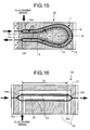
- FIG. 16 is a top plan view of an optical modulator that illustrates an example of the conventional optical device.
- This optical modulator 20 is a Mach-Zehnder interruption type optical modulator, and has a straight optical waveguide.
- a data line 22 that is supplied with an electronic signal such as DC is formed to have a predetermined length L0 in its longitudinal direction on a substrate 21. Both ends of the data line 22 are led out to one side of the substrate 21 respectively, and signal electrodes 22a and 22b are formed.
- a ground electrode 23 is formed on other partition of the substrate 21 excluding the data line 22.
- An optical waveguide 24 is disposed linearly along the data line 22, and two optical waveguides 24 are disposed in parallel between branch portions 24a and 24b.
- a phase difference due to mutual interference can be generated between the two optical waveguides 24 in a state that a speed of a progressive wave of the electronic signal (microwave) that is supplied to the data line 22 and a speed of an optical wave that flows through the two optical waveguides 24 are matched.
- a predetermined work length (corresponding to the length L0) is necessary as a length of the parallel two optical waveguides 24. A few centimeters are necessary for the length of L0.
- the curvature of the curved optical waveguide cannot be set small.
- the curvature of the curved optical waveguide is set small to a few millimeters, the recombining of the light becomes insufficient, and the optical loss increases remarkably.
- the curvature of the curved optical waveguide cannot be set small, the total optical waveguide cannot be made small, which makes it impossible to make small the optical device that is formed with the optical waveguide or to integrate the optical device.
- the optical device cannot be made compact.
- the present invention has been achieved in order to solve the above problems, and has an object of providing a compact optical waveguide, a compact optical device, and a method of manufacturing the optical waveguide capable of suppressing the optical loss.
- An optical waveguide that is formed on a substrate according to one aspect of the present invention includes a curved ridge structure that is formed on the substrate so as to have a curvature in a longitudinal direction of the curved ridge structure; a curved optical path that is formed along the curved ridge structure; and a buffer layer that covers a side of the curved ridge structure and that has a lower refractive index than a refractive index of the substrate.
- An optical device for performing phase modulation according to another aspect of the present invention includes an optical waveguide and a signal electrode.
- the optical waveguide includes a curved ridge structure that is formed on a substrate so as to have a curvature in a longitudinal direction of the curved ridge structure; a curved optical path that is formed in and along the curved ridge structure; and a buffer layer that covers a side of the ridge structure and that has a lower refractive index than a refractive index of the substrate.
- the signal electrode is disposed on and along the optical waveguide.
- a method of manufacturing an optical waveguide includes forming a pattern of titanium on a substrate, the pattern including a curved pattern for forming a curved optical path; thermally diffusing the pattern at a high temperature; forming a ridge structure by etching the substrate positioned at a side of the curved pattern, along a shape of the curved pattern; and forming a buffer layer on a side of the ridge structure, the buffer layer being made of a material that has a lower refractive index than a refractive index of the substrate.
- a method of manufacturing an optical waveguide includes forming a proton exchange pattern on a substrate by proton exchange, the pattern including a curved pattern for forming a curved optical path; forming a ridge structure by etching the substrate positioned at a side of the curved pattern, along a shape of the curved pattern; and forming a buffer layer on a side of the ridge structure, the buffer layer being made of a material that has a lower refractive index than a refractive index of the substrate.
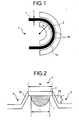
- Fig. 1 is a top plan view of the optical waveguide according to the first embodiment.
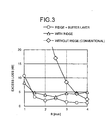
- Fig. 2 is a cross-sectional view of the optical waveguide shown in Fig. 1.
- Fig. 1 mainly illustrates a curved portion as a key portion of the optical waveguide.
- An optical waveguide 1 is a titanium diffusion lithium niobate (Ti-LiNbO 3 ) diffusion waveguide.
- a curved portion 1 a shown in the drawing has an arc shape with a central angle of 180 degrees.
- a pattern width L of the optical waveguide 1 is set to 5 to 9 micrometers to have a small mode field of light.
- An optical wave that propagates through the optical waveguide 1 is generally a single mode (hereinafter, "SM") light, but the optical propagation mode of the optical waveguide 1 according to this invention is not limited to the SM.
- SM single mode
- a substrate 2 is dug out to form a ridge structure 3 at both sides of at least the curved portion 1 a of the optical waveguide 1.
- the substrate 2 is etched to form the ridge structure 3.
- the power of the light that propagates through the optical waveguide 1 becomes a maximum at a position of about 3 micrometers from the surface. Therefore, a depth d of the ridge structure 3 that is formed by etching is set to equal to or larger than 3 micrometers.
- air reffractive index 1 corresponds to a cladding.
- the ridge structure 3 that is formed by digging down the substrate 2 has a rough surface and not smooth on the side surface 3a.
- an optical loss occurs at the curved portion 1a.
- a scattering loss becomes large among the optical loss.
- a film-shaped buffer layer 4 is formed on the surface of the side surface 3a of the ridge structure 3.
- a material having a smaller refractive index than that of the substrate 2 can be used such as silicon oxide (SiO 2 ) and titanium oxide (TiO 2 ).
- the width W of the ridge structure 3 is preferably equal to or smaller than the width L of the optical waveguide 1 plus 6 micrometers (i.e., both sides are equal to or less than 3 micrometers from the center of the optical waveguide 1 respectively).
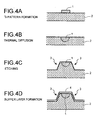
- Fig. 3 is a graph indicating the optical loss of the optical waveguide according to the present invention.
- the abscissa represents a curvature (a radius) R of the curved portion 1a of the optical waveguide 1
- the ordinate represents the optical loss (excessive loss).
- the optical loss can be suppressed even when the curvature R is set small to 4 millimeters or below.
- the optical loss is large in the total range of the curvature R equal to or smaller than 4 millimeters.
- the optical loss can be suppressed as compared with the conventional method.
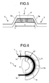
- Figs. 4A to 4D are illustrates for process of manufacturing the optical waveguide according to the present invention.
- a Ti pattern is first formed as shown in Fig. 4A.
- a resist pattern is formed along the layout of the optical waveguide 1 including the ridge structure 1a.
- the optical waveguide 1 is formed by etching.
- a thermal diffusion is then carried out as shown in Fig. 4B.
- the optical waveguide 1 of Ti is thermally diffused to have a cross section in approximately a semicircle shape inside the substrate 2.
- the optical waveguide 1 has a highest refractive index at approximately the center of the circle, and can guide the wave in confinement.
- the optical waveguide 1 can be formed by proton exchange in benzoic acid, in place of carrying out the thermal diffusion.
- the etching is carried out as shown in Fig. 4C.
- the ridge structure 3 is formed by digging out the substrate 2 positioned at least at the curved portion 1 a of the optical waveguide 1 by etching.
- This etching process may be a reactive ion etching (RIE) or the like.
- RIE reactive ion etching
- the width W and the height d required for the ridge structure 3 are satisfied based on the pattern width L (refer to Fig. 2) of the optical waveguide 1.
- a buffer layer is formed as shown in Fig. 4D.
- the buffer layer 4 is formed to cover the side surface 3a of the ridge structure 3 by sputtering or the like.
- the optical waveguide 1 can be formed in the state that the ridge structure 3 and the buffer layer 4 are formed on the substrate 2.
- the ridge structure 3 and the buffer layer 4 are provided on only the ridge structure 1 a of the optical waveguide 1, the ridge structure 3 and the buffer layer 4 may also be provided on a straight line portion that continues from the curved portion 1a.
- the optical waveguide 1 shown in Fig. 1 has the ridge structure 1a configured in the arc shape having a central angle of 180 degrees, the curve angle of the curved portion 1 a is not limited to this configuration.
- an output of the optical wave can be directed to a different direction from the input direction at an angle of 90 degrees or above.
- Fig. 5 is a cross-sectional view of a modification of the optical waveguide.
- the width L of the optical waveguide 1 coincides with the width of the ridge structure 3.
- This optical waveguide 1 is formed by expanding the width of the resist pattern to be larger than the width W of the ridge structure 3 at the time of forming the Ti pattern of the optical waveguide 1, and then executing a diffusion at the diffusion time so that the diffusion depth is approximately constant in a normal direction of the substrate.
- the optical waveguide 1 formed in this way has a flat surface as compared with the cross-sectional shape shown in Fig. 2.
- Fig. 6 is a top plan view of another modification of the optical waveguide.
- a pattern width L1 of the straight line portion 1 b and a pattern width L2 of the ridge structure 1 a may be differentiated in order to minimize the optical loss at respective positions.
- a coupler 5 is provided at a coupling portion between the straight line portion 1b and the curved portion 1 a.
- the coupler 5 shown in Fig. 6 is formed to have a stage.
- Fig. 7 is a partial top plan view of another example of a configuration of the transformation section. As shown in Fig. 7, the coupler 5 may be formed in tapered shape.
- Fig. 8 is a top plan view of still another modification of the optical waveguide.
- the position of the curved portion 1a of the optical waveguide 1 is shifted to the inside relative to the ridge structure 3.
- the position of the curved portion 1a is not limited to pass through the center of the ridge structure 3 as shown in Fig. 1.
- the curved portion 1a having the pattern width L is shifted toward the inside from the center of the ridge structure 3 having the width W. In this state, the internal periphery of the curved portion 1a is close to or is connected to the side surface 3a of the inside ridge structure 3.
- the external periphery of the curved portion 1a is separated from the side surface 3a of the outside ridge structure 3 by a predetermined distance.
- the curved portion 1a may be shifted to the outside, in addition to a configuration of shifting the curved portion 1a to the inside of the ridge structure 3.
- the shift is carried out by a predetermined amount to a direction of reducing the radiation loss.
- the radiation loss can be suppressed by setting a distance between the curved portion 1a and the side surface 3a of the ridge structure 3 that is disposed at the external peripheral side of the curved portion 1a.
- optical losses that are important in the optical waveguide are the radiation loss and the scattering loss.
- the width W of the ridge structure 3 is made smaller, the influence of the radiation loss can be decreased, but the influence of the scattering loss increases.
- the width W of the ridge structure 3 is made larger, the influence of the scattering loss can be decreased, but the influence of the radiation loss increases.
- the scattering loss occurs because of the roughness of the side surface 3a of the ridge structure 3 as described above. Based on this condition, the shift amount capable of suppressing the radiation loss without having the influence of the scattering loss can be set.
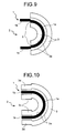
- Fig. 9 is a top plan view of still another modification of the optical waveguide.
- the center position of the curved portion 1a and the center position of the straight line portion 1b are shifted at the portion of the coupler 5.
- the coupling loss offset
- the coupling loss occurs due to the difference between the optical propagation state (field) of the straight line portion and the optical field of the curved portion.
- a configuration of shifting the mutual coupling by a predetermined amount is employed (for example, see Japanese Patent Application Laid-open No. H11-167032).
- the coupling loss can be suppressed by making the distributions of the field (or magnetic field) of the respective propagation light approximately equal.
- the coupling loss and the radiation loss of the curved portion 1 a can be suppressed.
- Fig. 9 also illustrates the configuration of shifting the center position of the curved portion 1a relative to the center position of the ridge structure 3 (refer to Fig. 8). In this way, the scattering loss and the radiation loss can be suppressed more.
- Fig. 10 is a top plan view of still another modification of the optical waveguide.
- the configuration shown in Fig. 10 is a modification of the ridge structure 3.
- a stage having a predetermined shift amount is formed in the ridge structure 3 at the coupling portion between the curved portion 1a and the straight line portion 1b of the optical waveguide 1.
- the width of the curved portion 1a and that of the straight line portion 1b that constitute the optical waveguide 1 are constant.
- Fig. 10 also illustrates the configuration of shifting the center position of the curved portion 1a relative to the center position of the ridge structure 3, in a similar manner to that shown in Fig. 9.
- the center position of the straight line portion 1b of the optical waveguide 1 coincides with the center position of the ridge structures 3c and 3d respectively that are provided at both sides of the straight line portion 1b.
- a stage having a predetermined shift amount is formed at the coupling portion between the ridge structure 3 of the curved portion 1a and the ridge structures 3c and 3d of the straight line portion 1b of the optical waveguide 1.
- the ridge structure 3 provided at the side of the optical waveguide 1 can be formed individually by matching the optimum layout state at the curved portion 1a with the optimum layout state at the straight line portion 1b.
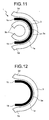
- Fig. 11 is a top plan view of still another modification of the optical waveguide.
- the configuration shown in Fig. 11 is a modification of the ridge structure 3.
- a coupling loss may occur at a starting point of the ridge, that is, at the coupling portion between the straight line portion 1b and the curved portion 1a of the optical waveguide 1 (i.e., the position of the coupler 5).
- the ridge structure 3 is not provided at only the curved portion 1a but is also stretched as extension portions 3c and 3d to a direction of the straight line portion 1b by a predetermined amount.
- the extension portions 3c and 3d are formed to gradually leave the straight line portion 1b as they leave the position of the coupling portion.
- the extension portion 3c positioned at the inside of the optical waveguide 1 is formed toward the inside at same curvature as that of the ridge structure 3.
- the extension portion 3d positioned at the outside of the optical waveguide 1 has the same curvature as that of the extension 3c, and is formed toward the outside.
- Fig. 12 is a top plan view of still another modification of the optical waveguide.
- Fig. 12 out of the extension portions explained with reference to Fig. 11, only the external extension portion 3d is provided.
- the extension portion 3d is provided on the ridge structure 3 that is positioned at the outside of the optical waveguide 1, the coupling loss can be minimized.
- optical device that uses the optical waveguide 1 explained in the first embodiment includes an optical switch and an optical modulator.
- Fig. 13 is a top plan view of an optical modulator as an optical device.
- This optical modulator has a curved portion at a part of the optical waveguide that is provided in the conventional Mach-Zehnder interference type optical modulator shown in Fig. 16.
- a data line 12 On a substrate 11 of an optical modulator 10 shown in Fig. 13, a data line 12, signal electrodes 12a and 12b, and a ground electrode 13 are provided.
- the data line 12 has a length that satisfies the length of the operation length L0, and has a curved portion that is curved in approximately a U-shape.
- the optical waveguide 1 is disposed along the data line 12, and branch portions 1c and 1d are formed on a portion that is superimposed with the data line 12. Two optical waveguides are disposed in parallel between these branch portions 1c and 1d.
- the optical waveguide 1 has the curved portion 1a and the straight line portion 1b in a similar manner to that of the first embodiment. These branch portions 1a and 1b become an interaction section between light and microwave.
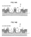
- Figs. 14A and 14B are cross-sectional views of the configuration shown in Fig. 13.
- the ridge structure 3 and the buffer layer 4 are provided over the whole length of the optical waveguide 1.
- the width W of the ridge structure 3 is constant at the curved portion 1a, thereby to make it possible to align the speed of the microwave with the speed of light over the whole region of the interaction section.
- the center position of the ridge structure 3 coincides with the center position of the optical waveguide 1, at the portion of the straight line portion 1b of the optical waveguide 1 (cross-section of A-A). Further, as shown in Fig.
- the center position of the optical waveguide 1 is disposed with a predetermined shift amount from the center position of the ridge structure 3 to a direction of the external ridge structure 3, at the portion of the curved portion 1a of the optical waveguide 1 (cross-section of B-B).
- the curved portion 1a of the optical waveguide 1 can also be shifted by a predetermined amount to the internal periphery side of the ridge structure 3 when the radiation loss can be reduced in this direction, in a similar manner to that explained above with reference to Fig. 8.
- the length in the lateral direction can be made shorter than the conventional length shown in Fig. 16, and the device can be made compact.
- Fig. 15 is a top pl.an view of another configuration example of the optical modulator as an optical device.
- the configuration is different from that shown in Fig. 13 in that the curvature of the curved portion 1a of the optical waveguide 1 is set large. Further, the total width (in the vertical direction in the drawing) is set small.
- the straight line portions 1b of the optical waveguide 1 for input and output are set closer to each other.
- approximately a half of a part of the straight line portion 1b facing the curved portion 1a side is not linear, and forms an arc portion 1e that connects between the curved portion 1 a and the straight line portion 1b.
- the optical waveguide 1 can be formed freely within a range of the size of the optical device (substrate 2) to match the size (vertical and lateral sizes) of the optical device and conditions of connector connection and the like.
- the ridge structure 3 and the buffer layer 4 are also formed along the optical waveguide 1 as shown in Fig. 14. With this arrangement, the optical loss (radiation loss and scattering loss) can be suppressed without depending on the shape of the optical waveguide 1.
- the optical waveguide 1 according to the second embodiment is explained taking the example of the configuration of an approximately the U-shape so that the input direction of an optical signal is turned to the output direction of the optical signal by 180 degrees at one position.
- the light input section and the output section of the optical waveguide 1 are disposed on the same one side surface of the optical device.
- the optical waveguide 1 can also have a configuration of approximately an S-shape having a turning at two positions or a turning at three or more positions.
- the work length L0 can be set long, and a variable region of a phase difference can be increased.
- the turning is provided by an even number of times, the light input section and the output section of the optical waveguide 1 are disposed on different side surfaces of the optical device.
- the optical waveguide 1 can also be applied to a phase modulator.
- the configuration of the phase modulator is different from that of the optical modulator only in that one optical waveguide is provided without using branch portions.
- This phase modulator also has electrodes disposed on the optical waveguide 1.
- the optical waveguide 1 explained above can also be applied to other electronic device such as an optical switch in addition to the optical modulator such as the phase modulator.
- the optical loss in the electronic device can also be suppressed, and the device can be made compact.
- a curved portion is formed on an optical waveguide. Even when a curvature of the curved portion is small, there is an effect that optical loss can be suppressed, and that the optical waveguide and an optical device using the optical waveguide can be made compact.
- an optical waveguide is formed on a substrate, comprising a curved ridge structure that is formed on the substrate so as to have a curvature in a longitudinal direction of the curved ridge structure, a curved optical path that is formed along the curved ridge structure, and a buffer layer that covers a side of the curved ridge structure and that has a lower refractive index than a refractive index of the substrate.
- the curved optical path is formed on a top side of the curved ridge structure.
- the curved ridge structure is formed outside the curved ridge structure.
- the buffer layer is silicon oxide.
- the substrate is made from lithium niobate.
- the curved optical path has a curvature of not more than 4 millimeters.
- the curved optical path has a width in a range from 5 micrometers to 9 micrometers.
- a width of the curved optical path is equal to a width of the curved ridge structure.
- the curved optical path has a turning angle in a range from 90 degrees to 180 degrees.
- a center line of the curved optical path is shifted from a center line of the curved ridge structure.
- the curved ridge structure has a width of at most 6 micrometers plus a width of the curved portion.
- the curved ridge structure has a height of at least 3 micrometers.
- the optical waveguide further comprises a straight optical path that is coupled with the curved optical path, a second ridge structure that is formed on the substrate along the straight optical path, and a second buffer layer that covers a side of the second ridge structure and that has a lower refractive index than a refractive index of the substrate, wherein the straight optical path is formed in and along the second ridge structure, and the second ridge structure has a width increased along the straight optical path.
- the optical waveguide further comprises an optical path that is coupled with the curved optical path and that has a width different from a width of the curved optical path, and a coupler that optically couples the curved optical path with the optical path.
- the coupler is an optical path whose width gradually changes from a width of the curved optical path to a width of the optical path.
- the optical waveguide further comprises an optical path that is coupled with the curved optical path and that has a width different from a width of the curved optical path, wherein the optical path is coupled with the curved optical path so that an axis of the optical path is shifted from an axis of the curved optical path.
- the optical waveguide further comprises a straight optical path that is coupled with the curved optical path, a second ridge structure that is formed on the substrate along the straight optical path, and second buffer layer that covers a side of the second ridge structure and that has a lower refractive index than a refractive index of the substrate, wherein the straight optical path is formed in and along the second ridge structure, and the second ridge structure is connected to the curved ridge structure so that an axis of the second ridge structure is shifted from an axis of the curved ridge structure.
- an optical device for performing phase modulation comprises an optical waveguide that includes a curved ridge structure that is formed on a substrate so as to have a curvature in a longitudinal direction of the curved ridge structure, a curved optical path that is formed in and along the curved ridge structure, and a buffer layer that covers a side of the ridge structure and that has a lower refractive index than a refractive index of the substrate, and a signal electrode that is disposed on and along the optical waveguide.
- the optical waveguide includes two optical paths that are parallel to each other, and the signal electrode is disposed on and along each of the two optical paths.
- the optical waveguide further includes a second ridge structure that is formed on the substrate straight in a longitudinal direction of the second ridge structure, a straight optical path that is coupled with the curved optical path and that is formed in and along the second ridge structure, and a second buffer layer that covers a side of the second ridge structure and that has a lower refractive index than a refractive index of the substrate, optical signals transmitted through the curved optical path and the straight optical path interact with electric signals transmitted through the signal electrode, and the curved ridge structure and the second ridge structure have a constant width.
- the optical waveguide further includes a first straight optical path that has an input end and a first connecting end that is coupled with one end of the curved optical path, and a second straight optical path that has an output end and a second connecting end is coupled with another end of the curved optical path, and that is parallel to the first straight optical path, and the input end and the output end are disposed on a side of the substrate.
- the curved optical path has a first curved portion and a second curved portion, the first curved portion has a constant curvature, and the second curved portion has a curvature gradually changing to be connected with one of the first connecting end and the second connecting end.
- a method of manufacturing an optical waveguide comprises forming a pattern of titanium on a substrate, the pattern including a curved pattern for forming a curved optical path, thermally diffusing the pattern at a high temperature, forming a ridge structure by etching the substrate positioned at a side of the curved pattern, along a shape of the curved pattern, and forming a buffer layer on a side of the ridge structure, the buffer layer being made of a material that has a lower refractive index than a refractive index of the substrate.
- a method of manufacturing an optical waveguide comprises forming a proton exchange pattern on a substrate by proton exchange, the pattern including a curved pattern for forming a curved optical path, forming a ridge structure by etching the substrate positioned at a side of the curved pattern, along a shape of the curved pattern, and forming a buffer layer on a side of the ridge structure, the buffer layer being made of a material that has a lower refractive index than a refractive index of the substrate.
Landscapes
- Physics & Mathematics (AREA)
- General Physics & Mathematics (AREA)
- Optics & Photonics (AREA)
- Engineering & Computer Science (AREA)
- Microelectronics & Electronic Packaging (AREA)
- Nonlinear Science (AREA)
- Power Engineering (AREA)
- Electromagnetism (AREA)
- Optical Integrated Circuits (AREA)
- Optical Modulation, Optical Deflection, Nonlinear Optics, Optical Demodulation, Optical Logic Elements (AREA)
Abstract
Description
Claims (17)
- An optical waveguide that is formed on a substrate, comprising:characterized by further comprisinga curved ridge structure (3) that is formed on the substrate (2) so as to have a curvature in a longitudinal direction of the curved ridge structure (3); anda curved optical path (1, 1a) that is formed along the curved ridge structure,
a buffer layer (4) that covers a side (3a) of the curved ridge structure (3) and that has a lower refractive index than a refractive index of the substrate sandwiched between the curved optical path (1, 1a) and the buffer layer (4). - The optical waveguide according to claim 1, wherein the curved optical path (1, 1a) is formed on a top side of the curved ridge structure (3).
- The optical waveguide according to claim 1, wherein a further curved ridge structure (3) is formed outside the curved ridge structure (3).
- The optical waveguide according to claim 1, wherein the buffer layer (4) is silicon oxide.
- The optical waveguide according to claim 1, wherein the substrate (2) is made from lithium niobate.
- The optical waveguide according to claim 1, wherein the curved optical path (1, 1a) has a curvature of not more than 4 millimeters.
- The optical waveguide according to claim 1, wherein the curved optical path (1, 1a) has a width in a range from 5 micrometers to 9 micrometers.
- The optical waveguide according to claim 1, wherein a width of the curved optical path (1, 1a) is equal to a width of the curved ridge structure (3).
- The optical waveguide according to claim 1, wherein the curved optical path (1, 1a) has a turning angle in a range from 90 degrees to 180 degrees.
- The optical waveguide according to claim 1, wherein a center line of the curved optical path (1, 1a) is shifted from a center line of the curved ridge structure (3).
- The optical waveguide according to claim 1, wherein the curved ridge structure (3) has a width of at most the sum of 6 micrometers plus a width of the optical path (1, 1a).
- The optical waveguide according to claim 1, wherein the curved ridge structure (3) has a height of at least 3 micrometers.
- The optical waveguide according to claim 1, further comprising:a straight optical path (1, 1b) that is coupled with the curved optical path;a second ridge structure (3) that is formed on the substrate along the straight optical path (1, 1b); anda second buffer layer (4) that covers a side of the second ridge structure (3) and that has a lower refractive index than a refractive index of the substrate (2), whereinthe straight optical path (1, 1b) is formed in and along the second ridge structure (3), andthe second ridge structure (3) has a width increased along the straight optical path (1, 1b).
- The optical waveguide according to claim 1, further comprising:an optical path (1, 1b) that is coupled with the curved optical path (1, 1a) and that has a width different from a width of the curved optical path (1, 1a); anda coupler (5) that optically couples the curved optical path (1, 1a) with the optical path (1, 1b).
- The optical waveguide according to claim 14, wherein the coupler (5) is an optical path (1, 1b) whose width gradually changes from a width of the curved optical path (1, 1a) to a width of the optical path (1, 1b).
- The optical waveguide according to claim 1, further comprising an optical path (1, 1b) that is coupled with the curved optical path (1, 1a) and that has a width different from a width of the curved optical path (1, 1a), wherein
the optical path (1, 1b) is coupled with the curved optical path (1, 1a) so that an axis of the optical path (1, 1b) is shifted from an axis of the curved optical path (1, 1a). - The optical waveguide according to claim 1, further comprising:a straight optical path (1, 1b) that is coupled with the curved optical path (1, 1a);a second ridge structure (3, 3c, 3d) that is formed on the substrate (2) along the straight optical path (1, 1b); anda second buffer layer (4) that covers a side of the second ridge structure (3, 3c, 3d) and that has a lower refractive index than a refractive index of the substrate (2), whereinthe straight optical path (1, 1b) is formed in and along the second ridge structure (3, 3c, 3d), andthe second ridge structure (3, 3c, 3d) is connected to the curved ridge structure (3) so that an axis of the second ridge structure (3, 3c, 3d) is shifted from an axis of the curved ridge structure (3).
Applications Claiming Priority (3)
| Application Number | Priority Date | Filing Date | Title |
|---|---|---|---|
| JP2003079116A JP2004287093A (en) | 2003-03-20 | 2003-03-20 | Optical waveguide, optical device, and method of manufacturing optical waveguide |
| JP2003079116 | 2003-03-20 | ||
| EP04002068A EP1460458B1 (en) | 2003-03-20 | 2004-01-30 | Curved ridge optical waveguide, optical device, and method of manufacturing optical waveguide |
Related Parent Applications (2)
| Application Number | Title | Priority Date | Filing Date |
|---|---|---|---|
| EP04002068.7 Division | 2004-01-30 | ||
| EP04002068A Division EP1460458B1 (en) | 2003-03-20 | 2004-01-30 | Curved ridge optical waveguide, optical device, and method of manufacturing optical waveguide |
Publications (3)
| Publication Number | Publication Date |
|---|---|
| EP1589360A2 true EP1589360A2 (en) | 2005-10-26 |
| EP1589360A3 EP1589360A3 (en) | 2005-11-02 |
| EP1589360B1 EP1589360B1 (en) | 2009-09-23 |
Family
ID=32821406
Family Applications (3)
| Application Number | Title | Priority Date | Filing Date |
|---|---|---|---|
| EP04002068A Expired - Lifetime EP1460458B1 (en) | 2003-03-20 | 2004-01-30 | Curved ridge optical waveguide, optical device, and method of manufacturing optical waveguide |
| EP05013464A Expired - Lifetime EP1589360B1 (en) | 2003-03-20 | 2004-01-30 | Curved ridge optical waveguide, optical device, and method of manufacturing optical waveguide |
| EP06014368.2A Expired - Lifetime EP1705515B1 (en) | 2003-03-20 | 2004-01-30 | Curved ridge optical waveguide, optical device, and method of manufacturing optical waveguide |
Family Applications Before (1)
| Application Number | Title | Priority Date | Filing Date |
|---|---|---|---|
| EP04002068A Expired - Lifetime EP1460458B1 (en) | 2003-03-20 | 2004-01-30 | Curved ridge optical waveguide, optical device, and method of manufacturing optical waveguide |
Family Applications After (1)
| Application Number | Title | Priority Date | Filing Date |
|---|---|---|---|
| EP06014368.2A Expired - Lifetime EP1705515B1 (en) | 2003-03-20 | 2004-01-30 | Curved ridge optical waveguide, optical device, and method of manufacturing optical waveguide |
Country Status (4)
| Country | Link |
|---|---|
| US (2) | US7054512B2 (en) |
| EP (3) | EP1460458B1 (en) |
| JP (1) | JP2004287093A (en) |
| DE (1) | DE602004023276D1 (en) |
Families Citing this family (44)
| Publication number | Priority date | Publication date | Assignee | Title |
|---|---|---|---|---|
| US7212326B2 (en) | 2003-05-30 | 2007-05-01 | Jds Uniphase Corporation | Optical external modulator |
| US7171063B2 (en) * | 2004-12-01 | 2007-01-30 | Jds Uniphase Corporation | Controllable electro-optic device having substrate trenches between electrodes |
| JP2007133135A (en) * | 2005-11-10 | 2007-05-31 | Ngk Insulators Ltd | Optical waveguide device |
| WO2007058366A1 (en) * | 2005-11-16 | 2007-05-24 | Ngk Insulators, Ltd. | Optical waveguide device |
| JP2007328257A (en) * | 2006-06-09 | 2007-12-20 | Fujitsu Ltd | Optical waveguide, optical device, and optical waveguide manufacturing method |
| JP2008026374A (en) * | 2006-07-18 | 2008-02-07 | Fujitsu Ltd | Optical waveguide, optical device, and optical waveguide manufacturing method |
| JP4899730B2 (en) * | 2006-09-06 | 2012-03-21 | 富士通株式会社 | Light modulator |
| JP5123528B2 (en) * | 2007-01-11 | 2013-01-23 | 富士通オプティカルコンポーネンツ株式会社 | Optical waveguide, optical device, and optical waveguide manufacturing method |
| JP5117082B2 (en) * | 2007-03-08 | 2013-01-09 | アンリツ株式会社 | Light modulator |
| WO2008111407A1 (en) | 2007-03-09 | 2008-09-18 | Nec Corporation | Thermo-optical phase shifter |
| JP5076726B2 (en) * | 2007-08-13 | 2012-11-21 | 富士通株式会社 | Optical modulator and optical transmitter |
| JPWO2009090687A1 (en) * | 2008-01-18 | 2011-05-26 | アンリツ株式会社 | Light modulator |
| WO2009096237A1 (en) * | 2008-01-31 | 2009-08-06 | Ngk Insulators, Ltd. | Optical waveguide device |
| JP5374882B2 (en) * | 2008-02-08 | 2013-12-25 | 富士通株式会社 | Optical device |
| JP4842987B2 (en) * | 2008-03-19 | 2011-12-21 | 富士通株式会社 | Optical device |
| JP5320840B2 (en) * | 2008-06-17 | 2013-10-23 | 富士通株式会社 | Optical device and manufacturing method thereof |
| JP4992837B2 (en) | 2008-06-30 | 2012-08-08 | 富士通株式会社 | Optical device manufacturing method |
| JP2010151973A (en) * | 2008-12-24 | 2010-07-08 | Fujitsu Ltd | Optical semiconductor device, manufacturing method thereof, and optical transmission device |
| JP5176150B2 (en) | 2009-01-13 | 2013-04-03 | 富士通株式会社 | Optical device and optical transmitter |
| JP2012008160A (en) * | 2010-06-22 | 2012-01-12 | Nec Corp | Optical waveguide device and method for manufacturing optical waveguide device |
| JP5195998B2 (en) * | 2011-11-30 | 2013-05-15 | 富士通株式会社 | Optical device |
| JP5708465B2 (en) * | 2011-12-12 | 2015-04-30 | 日立金属株式会社 | Optical fiber connection component and optical fiber connection module |
| TW201426151A (en) * | 2012-12-19 | 2014-07-01 | Hon Hai Prec Ind Co Ltd | Electro-optical modulator |
| US9696015B2 (en) | 2014-07-23 | 2017-07-04 | Powerarc, Inc. | Changeable emergency warning light assembly |
| US9638981B2 (en) * | 2015-02-24 | 2017-05-02 | Huawei Technologies Co., Ltd. | Optical switch with improved switching efficiency |
| GB2558307B (en) * | 2016-12-30 | 2021-05-05 | Lumentum Tech Uk Limited | Waveguide array |
| JP7115483B2 (en) * | 2017-08-24 | 2022-08-09 | Tdk株式会社 | optical modulator |
| JP6950400B2 (en) | 2017-09-22 | 2021-10-13 | 住友電気工業株式会社 | Mach Zenda Modulator |
| JP7027787B2 (en) * | 2017-10-13 | 2022-03-02 | Tdk株式会社 | Optical modulator |
| WO2019082347A1 (en) * | 2017-10-26 | 2019-05-02 | フォトンリサーチ株式会社 | Light guide device, optical waveguide device, multi-wavelength light source module, and method for manufacturing optical waveguide device |
| JP7397567B2 (en) | 2017-12-20 | 2023-12-13 | 富士通オプティカルコンポーネンツ株式会社 | Optical modulator and optical module |
| JP7056236B2 (en) * | 2018-03-02 | 2022-04-19 | 富士通オプティカルコンポーネンツ株式会社 | Optical modulators and optical transceiver modules using them |
| JP7117869B2 (en) * | 2018-03-22 | 2022-08-15 | 株式会社日立製作所 | Analysis equipment |
| US12080651B2 (en) | 2018-03-27 | 2024-09-03 | Nielson Scientific, Llc | Three-dimensional micro-electro-mechanical, microfluidic, and micro-optical systems |
| JP2019219484A (en) * | 2018-06-19 | 2019-12-26 | 日本電気株式会社 | Polarization cleaner and optical module |
| JP2020134876A (en) * | 2019-02-25 | 2020-08-31 | Tdk株式会社 | Electro-optical element |
| JP7183878B2 (en) * | 2019-03-13 | 2022-12-06 | 住友大阪セメント株式会社 | optical waveguide element |
| CN111863590B (en) * | 2019-04-24 | 2023-05-16 | 世界先进积体电路股份有限公司 | Substrate structure and method for manufacturing semiconductor structure comprising same |
| US10935738B1 (en) | 2019-08-08 | 2021-03-02 | Stmicroelectronics S.R.L. | Architecture of an integrated optics device |
| US10989872B1 (en) * | 2019-10-18 | 2021-04-27 | Globalfoundries U.S. Inc. | Waveguide bends with mode confinement |
| US12306438B2 (en) | 2019-11-26 | 2025-05-20 | Nippon Telegraph And Telephone Corporation | Optical waveguide |
| JP7447559B2 (en) | 2020-03-05 | 2024-03-12 | 富士通オプティカルコンポーネンツ株式会社 | Optical devices and optical transceivers |
| CN111240052B (en) * | 2020-03-10 | 2023-03-21 | Nano科技(北京)有限公司 | Coplanar waveguide transmission line and silicon-based electro-optic modulator with same |
| CN119087580B (en) * | 2024-09-29 | 2025-09-30 | 华中科技大学 | An optical gyroscope integrated chip based on thin-film lithium niobate photonic integration platform |
Family Cites Families (48)
| Publication number | Priority date | Publication date | Assignee | Title |
|---|---|---|---|---|
| US4116530A (en) * | 1976-07-29 | 1978-09-26 | Texas Instruments Incorporated | Optical waveguides grown by selective liquid phase epitaxy |
| JP2594895B2 (en) * | 1983-07-08 | 1997-03-26 | 株式会社日立製作所 | Method for manufacturing optical integrated circuit device |
| JPS6053904A (en) | 1983-09-05 | 1985-03-28 | Hitachi Ltd | Ridge type light guide |
| JPH0627914B2 (en) * | 1985-03-15 | 1994-04-13 | 日本放送協会 | Optical element |
| US4827866A (en) * | 1986-02-24 | 1989-05-09 | Northrop Corporation | Method and apparatus for treating an article in a heated environment |
| US4810049A (en) | 1987-04-02 | 1989-03-07 | American Telephone And Telegraph Company, At&T Bell Laboratories | Reducing bend and coupling losses in integrated optical waveguides |
| US4851368A (en) * | 1987-12-04 | 1989-07-25 | Cornell Research Foundation, Inc. | Method of making travelling wave semi-conductor laser |
| DE68920537T2 (en) | 1988-10-11 | 1995-06-14 | Sony Corp | Optical wavelength conversion devices. |
| JPH05297333A (en) | 1992-04-20 | 1993-11-12 | Sumitomo Cement Co Ltd | Optical modulator |
| US5216727A (en) | 1992-05-08 | 1993-06-01 | At&T Bell Laboratories | Integrated nonlinear waveguide spectrometer |
| JPH06209293A (en) | 1992-07-31 | 1994-07-26 | American Teleph & Telegr Co <Att> | Modulator in optical transmission system |
| US5455876A (en) * | 1992-10-23 | 1995-10-03 | General Microwave Israel Corporation | High-speed external integrated optical modulator |
| FR2715232B1 (en) * | 1994-01-19 | 1996-02-16 | Commissariat Energie Atomique | Method for optimizing a path of an optical guide and optical guide obtained by this method. |
| AU686318B2 (en) * | 1994-05-20 | 1998-02-05 | Iot Integrierte Optik Gmbh | Integrated optical branching arrangement |
| JPH0954291A (en) | 1995-08-11 | 1997-02-25 | Nippon Telegr & Teleph Corp <Ntt> | Optical phase shifter and optical switch using the same |
| JPH09145943A (en) * | 1995-11-28 | 1997-06-06 | Mitsubishi Gas Chem Co Inc | Curved optical waveguide and method of manufacturing the same |
| JPH09218384A (en) | 1996-02-14 | 1997-08-19 | Nippon Telegr & Teleph Corp <Ntt> | Light control element and method of using the same |
| JP3446929B2 (en) | 1996-09-18 | 2003-09-16 | 日本電信電話株式会社 | Semiconductor polarization rotator |
| JPH1114850A (en) | 1997-06-23 | 1999-01-22 | Oki Electric Ind Co Ltd | Manufacture of optical element |
| JPH1114849A (en) | 1997-06-23 | 1999-01-22 | Oki Electric Ind Co Ltd | Manufacturing method of optical element |
| JP4012367B2 (en) * | 1997-08-04 | 2007-11-21 | インターナショナル・ビジネス・マシーンズ・コーポレーション | Single-mode optical waveguide coupling element |
| JPH1152155A (en) | 1997-08-05 | 1999-02-26 | Oki Electric Ind Co Ltd | Optical waveguide having ridge structure and its production |
| JPH1164664A (en) | 1997-08-27 | 1999-03-05 | Oki Electric Ind Co Ltd | Production of optical waveguide |
| US6044098A (en) | 1997-08-29 | 2000-03-28 | Xerox Corporation | Deep native oxide confined ridge waveguide semiconductor lasers |
| US5991475A (en) * | 1997-09-26 | 1999-11-23 | Gte Laboratories Incorporated | Tightly curved digital optical switches |
| JPH11167032A (en) | 1997-12-03 | 1999-06-22 | Nippon Telegr & Teleph Corp <Ntt> | Bent optical waveguide circuit |
| JP2000147289A (en) | 1998-11-13 | 2000-05-26 | Nippon Telegr & Teleph Corp <Ntt> | Optical waveguide and method of manufacturing the same |
| AU779759B2 (en) * | 1999-05-21 | 2005-02-10 | Ipg Photonics Corporation | Planar optical waveguides with double grooves |
| JP2001004851A (en) | 1999-06-24 | 2001-01-12 | Kdd Corp | Optical circuit |
| US6614966B2 (en) * | 2000-03-22 | 2003-09-02 | Matsushita Electric Industrial Co., Ltd. | Optical waveguide device integrated module and method of manufacturing the same |
| JP4318381B2 (en) * | 2000-04-27 | 2009-08-19 | 本田技研工業株式会社 | Manufacturing method of fuselage structure made of fiber reinforced composite material, and fuselage structure manufactured thereby |
| US6304685B1 (en) * | 2000-05-05 | 2001-10-16 | The United States Of America As Represented By The Secretary Of The Navy | Low drive voltage LiNbO3 intensity modulator with reduced electrode loss |
| JP2001318253A (en) | 2000-05-12 | 2001-11-16 | Furukawa Electric Co Ltd:The | Optical waveguide directional coupler and optical waveguide circuit using the optical waveguide directional coupler |
| KR100763829B1 (en) * | 2000-06-08 | 2007-10-05 | 니치아 카가쿠 고교 가부시키가이샤 | Semiconductor laser device, and method of manufacturing the same |
| US6579068B2 (en) * | 2000-08-09 | 2003-06-17 | California Institute Of Technology | Method of manufacture of a suspended nitride membrane and a microperistaltic pump using the same |
| US20020048433A1 (en) * | 2000-10-10 | 2002-04-25 | Chi Wu | Optical component having a protected ridge |
| JP2004512551A (en) | 2000-10-13 | 2004-04-22 | マサチューセッツ インスティテュート オブ テクノロジー | Optical waveguide having trench structure |
| ATE403885T1 (en) | 2000-10-27 | 2008-08-15 | Pirelli & C Spa | HYBRID PLANAR BURNED/BRIDGE WAVEGUIDES |
| US6580843B2 (en) * | 2001-04-05 | 2003-06-17 | Fujitsu Limited | Optical device |
| JP2005508513A (en) * | 2001-04-27 | 2005-03-31 | サーノフ・コーポレーション | Optical waveguide crossing and method of forming the same |
| JP2002328348A (en) | 2001-04-27 | 2002-11-15 | Toshiba Corp | Optical modulator and alternating phased pulse generator |
| JP2002350915A (en) | 2001-05-30 | 2002-12-04 | Ngk Insulators Ltd | Wavelength transformation element, optical waveguide device for wavelength transformation, harmonic component generating device and method for manufacturing wavelength transformation element |
| US6680961B2 (en) * | 2001-08-01 | 2004-01-20 | Binoptics, Inc. | Curved waveguide ring laser |
| US20030044152A1 (en) * | 2001-09-04 | 2003-03-06 | Redfern Integrated Optics Pty Ltd | Waveguide formation |
| JP2003307603A (en) * | 2002-02-15 | 2003-10-31 | Omron Corp | Optical element and optical component using the element |
| JP2003264334A (en) * | 2002-03-08 | 2003-09-19 | Hitachi Ltd | Semiconductor laser device and semiconductor laser module |
| JP3543138B2 (en) * | 2002-04-24 | 2004-07-14 | Tdk株式会社 | Optical branch circuit and device |
| US20040184704A1 (en) * | 2003-03-17 | 2004-09-23 | Bakir Muhannad S. | Curved metal-polymer dual-mode/function optical and electrical interconnects, methods of fabrication thereof, and uses thereof |
-
2003
- 2003-03-20 JP JP2003079116A patent/JP2004287093A/en active Pending
-
2004
- 2004-01-29 US US10/766,019 patent/US7054512B2/en not_active Expired - Lifetime
- 2004-01-30 EP EP04002068A patent/EP1460458B1/en not_active Expired - Lifetime
- 2004-01-30 EP EP05013464A patent/EP1589360B1/en not_active Expired - Lifetime
- 2004-01-30 DE DE602004023276T patent/DE602004023276D1/en not_active Expired - Lifetime
- 2004-01-30 EP EP06014368.2A patent/EP1705515B1/en not_active Expired - Lifetime
-
2006
- 2006-01-30 US US11/341,593 patent/US7177490B2/en not_active Expired - Lifetime
Also Published As
| Publication number | Publication date |
|---|---|
| DE602004023276D1 (en) | 2009-11-05 |
| US20060133726A1 (en) | 2006-06-22 |
| EP1705515A3 (en) | 2006-10-18 |
| US7054512B2 (en) | 2006-05-30 |
| EP1460458B1 (en) | 2011-07-20 |
| JP2004287093A (en) | 2004-10-14 |
| EP1589360A3 (en) | 2005-11-02 |
| EP1460458A1 (en) | 2004-09-22 |
| EP1705515B1 (en) | 2013-08-28 |
| EP1589360B1 (en) | 2009-09-23 |
| EP1705515A2 (en) | 2006-09-27 |
| US7177490B2 (en) | 2007-02-13 |
| US20040184755A1 (en) | 2004-09-23 |
Similar Documents
| Publication | Publication Date | Title |
|---|---|---|
| US7054512B2 (en) | Optical waveguide, optical device, and method of manufacturing optical waveguide | |
| US7787717B2 (en) | Optical waveguide device | |
| CN114325939B (en) | Optical waveguide elements and optical modulation devices and optical transmission devices using optical waveguide elements | |
| US20050175271A1 (en) | Optical modulator | |
| CN101620296A (en) | High confinement waveguide on an electro-optic substrate | |
| JP2017129834A (en) | Optical waveguide element and optical modulator using the same | |
| JP2007072433A (en) | Optical integrated device and optical control device | |
| CN112711093B (en) | Polarization beam splitter structure and polarization beam splitting method | |
| JP5467414B2 (en) | Optical functional waveguide | |
| JP2007212787A (en) | Light control element, light switching unit and light modulator | |
| US7167607B2 (en) | Symmetric optical modulator with low driving voltage | |
| US8311371B2 (en) | Optical modulation device | |
| CN117092836A (en) | Electro-optical switch | |
| JP2007328257A (en) | Optical waveguide, optical device, and optical waveguide manufacturing method | |
| JP2001350046A (en) | Integrated optical waveguide element | |
| JP5123528B2 (en) | Optical waveguide, optical device, and optical waveguide manufacturing method | |
| US7463808B2 (en) | Optical waveguide, optical device, and manufacturing method of the optical waveguide | |
| EP1840633A1 (en) | Waveguide-type optical device | |
| RU2781367C1 (en) | Hybrid integrated optical device | |
| JP6260631B2 (en) | Optical waveguide device | |
| WO2026019362A1 (en) | An optical modulator | |
| WO2025137638A1 (en) | Multilayer thin film lithium-containing optical devices | |
| CN121432627A (en) | Fabrication method of silicon-based integrated magneto-optical waveguide, silicon-based integrated magneto-optical waveguide and isolator | |
| WO2024201876A1 (en) | Optical waveguide element and optical modulation device using same, and optical transmission device | |
| CN118409392A (en) | Optical waveguide element, optical modulation device using the optical waveguide element, and optical transmission device |
Legal Events
| Date | Code | Title | Description |
|---|---|---|---|
| PUAI | Public reference made under article 153(3) epc to a published international application that has entered the european phase |
Free format text: ORIGINAL CODE: 0009012 |
|
| PUAL | Search report despatched |
Free format text: ORIGINAL CODE: 0009013 |
|
| 17P | Request for examination filed |
Effective date: 20050622 |
|
| AC | Divisional application: reference to earlier application |
Ref document number: 1460458 Country of ref document: EP Kind code of ref document: P |
|
| AK | Designated contracting states |
Kind code of ref document: A2 Designated state(s): AT BE BG CH CY CZ DE DK EE ES FI FR GB GR HU IE IS IT LI LT LU MC NL PL PT RO SE SI SK TR |
|
| AX | Request for extension of the european patent |
Extension state: AL BA HR LV MK YU |
|
| AK | Designated contracting states |
Kind code of ref document: A3 Designated state(s): AT BE BG CH CY CZ DE DK EE ES FI FR GB GR HU IE IS IT LI LT LU MC NL PL PT RO SE SI SK TR |
|
| AX | Request for extension of the european patent |
Extension state: AL BA HR LV MK YU |
|
| AKX | Designation fees paid |
Designated state(s): DE FR GB |
|
| 17Q | First examination report despatched |
Effective date: 20060217 |
|
| GRAP | Despatch of communication of intention to grant a patent |
Free format text: ORIGINAL CODE: EPIDOSNIGR1 |
|
| GRAS | Grant fee paid |
Free format text: ORIGINAL CODE: EPIDOSNIGR3 |
|
| GRAA | (expected) grant |
Free format text: ORIGINAL CODE: 0009210 |
|
| AC | Divisional application: reference to earlier application |
Ref document number: 1460458 Country of ref document: EP Kind code of ref document: P |
|
| AK | Designated contracting states |
Kind code of ref document: B1 Designated state(s): DE FR GB |
|
| REG | Reference to a national code |
Ref country code: GB Ref legal event code: FG4D |
|
| REF | Corresponds to: |
Ref document number: 602004023276 Country of ref document: DE Date of ref document: 20091105 Kind code of ref document: P |
|
| PLBE | No opposition filed within time limit |
Free format text: ORIGINAL CODE: 0009261 |
|
| STAA | Information on the status of an ep patent application or granted ep patent |
Free format text: STATUS: NO OPPOSITION FILED WITHIN TIME LIMIT |
|
| 26N | No opposition filed |
Effective date: 20100624 |
|
| REG | Reference to a national code |
Ref country code: FR Ref legal event code: PLFP Year of fee payment: 13 |
|
| PGFP | Annual fee paid to national office [announced via postgrant information from national office to epo] |
Ref country code: FR Payment date: 20151208 Year of fee payment: 13 |
|
| PGFP | Annual fee paid to national office [announced via postgrant information from national office to epo] |
Ref country code: DE Payment date: 20160127 Year of fee payment: 13 |
|
| PGFP | Annual fee paid to national office [announced via postgrant information from national office to epo] |
Ref country code: GB Payment date: 20160127 Year of fee payment: 13 |
|
| REG | Reference to a national code |
Ref country code: DE Ref legal event code: R119 Ref document number: 602004023276 Country of ref document: DE |
|
| GBPC | Gb: european patent ceased through non-payment of renewal fee |
Effective date: 20170130 |
|
| REG | Reference to a national code |
Ref country code: FR Ref legal event code: ST Effective date: 20170929 |
|
| PG25 | Lapsed in a contracting state [announced via postgrant information from national office to epo] |
Ref country code: FR Free format text: LAPSE BECAUSE OF NON-PAYMENT OF DUE FEES Effective date: 20170131 |
|
| PG25 | Lapsed in a contracting state [announced via postgrant information from national office to epo] |
Ref country code: GB Free format text: LAPSE BECAUSE OF NON-PAYMENT OF DUE FEES Effective date: 20170130 Ref country code: DE Free format text: LAPSE BECAUSE OF NON-PAYMENT OF DUE FEES Effective date: 20170801 |