EP1587215A1 - Image data transmission circuit and image data display system - Google Patents
Image data transmission circuit and image data display system Download PDFInfo
- Publication number
- EP1587215A1 EP1587215A1 EP05008348A EP05008348A EP1587215A1 EP 1587215 A1 EP1587215 A1 EP 1587215A1 EP 05008348 A EP05008348 A EP 05008348A EP 05008348 A EP05008348 A EP 05008348A EP 1587215 A1 EP1587215 A1 EP 1587215A1
- Authority
- EP
- European Patent Office
- Prior art keywords
- image data
- pulse width
- electric current
- circuit
- width modulation
- Prior art date
- Legal status (The legal status is an assumption and is not a legal conclusion. Google has not performed a legal analysis and makes no representation as to the accuracy of the status listed.)
- Withdrawn
Links
- 230000005540 biological transmission Effects 0.000 title claims abstract description 92
- 230000006866 deterioration Effects 0.000 abstract description 5
- 230000003111 delayed effect Effects 0.000 description 8
- 230000008054 signal transmission Effects 0.000 description 8
- 238000010586 diagram Methods 0.000 description 5
- 101100191136 Arabidopsis thaliana PCMP-A2 gene Proteins 0.000 description 4
- 101100048260 Saccharomyces cerevisiae (strain ATCC 204508 / S288c) UBX2 gene Proteins 0.000 description 4
- 230000005855 radiation Effects 0.000 description 3
- 101100268335 Solanum lycopersicum TFT9 gene Proteins 0.000 description 2
- 230000005670 electromagnetic radiation Effects 0.000 description 2
- 230000003071 parasitic effect Effects 0.000 description 2
- 239000003990 capacitor Substances 0.000 description 1
- 230000001419 dependent effect Effects 0.000 description 1
- 230000001627 detrimental effect Effects 0.000 description 1
- 238000007599 discharging Methods 0.000 description 1
- 230000000694 effects Effects 0.000 description 1
- 239000011159 matrix material Substances 0.000 description 1
- 239000010409 thin film Substances 0.000 description 1
Images



Classifications
-
- G—PHYSICS
- G09—EDUCATION; CRYPTOGRAPHY; DISPLAY; ADVERTISING; SEALS
- G09G—ARRANGEMENTS OR CIRCUITS FOR CONTROL OF INDICATING DEVICES USING STATIC MEANS TO PRESENT VARIABLE INFORMATION
- G09G3/00—Control arrangements or circuits, of interest only in connection with visual indicators other than cathode-ray tubes
- G09G3/20—Control arrangements or circuits, of interest only in connection with visual indicators other than cathode-ray tubes for presentation of an assembly of a number of characters, e.g. a page, by composing the assembly by combination of individual elements arranged in a matrix no fixed position being assigned to or needed to be assigned to the individual characters or partial characters
- G09G3/22—Control arrangements or circuits, of interest only in connection with visual indicators other than cathode-ray tubes for presentation of an assembly of a number of characters, e.g. a page, by composing the assembly by combination of individual elements arranged in a matrix no fixed position being assigned to or needed to be assigned to the individual characters or partial characters using controlled light sources
- G09G3/30—Control arrangements or circuits, of interest only in connection with visual indicators other than cathode-ray tubes for presentation of an assembly of a number of characters, e.g. a page, by composing the assembly by combination of individual elements arranged in a matrix no fixed position being assigned to or needed to be assigned to the individual characters or partial characters using controlled light sources using electroluminescent panels
- G09G3/32—Control arrangements or circuits, of interest only in connection with visual indicators other than cathode-ray tubes for presentation of an assembly of a number of characters, e.g. a page, by composing the assembly by combination of individual elements arranged in a matrix no fixed position being assigned to or needed to be assigned to the individual characters or partial characters using controlled light sources using electroluminescent panels semiconductive, e.g. using light-emitting diodes [LED]
- G09G3/3208—Control arrangements or circuits, of interest only in connection with visual indicators other than cathode-ray tubes for presentation of an assembly of a number of characters, e.g. a page, by composing the assembly by combination of individual elements arranged in a matrix no fixed position being assigned to or needed to be assigned to the individual characters or partial characters using controlled light sources using electroluminescent panels semiconductive, e.g. using light-emitting diodes [LED] organic, e.g. using organic light-emitting diodes [OLED]
- G09G3/3275—Details of drivers for data electrodes
- G09G3/3283—Details of drivers for data electrodes in which the data driver supplies a variable data current for setting the current through, or the voltage across, the light-emitting elements
-
- G—PHYSICS
- G09—EDUCATION; CRYPTOGRAPHY; DISPLAY; ADVERTISING; SEALS
- G09G—ARRANGEMENTS OR CIRCUITS FOR CONTROL OF INDICATING DEVICES USING STATIC MEANS TO PRESENT VARIABLE INFORMATION
- G09G3/00—Control arrangements or circuits, of interest only in connection with visual indicators other than cathode-ray tubes
- G09G3/20—Control arrangements or circuits, of interest only in connection with visual indicators other than cathode-ray tubes for presentation of an assembly of a number of characters, e.g. a page, by composing the assembly by combination of individual elements arranged in a matrix no fixed position being assigned to or needed to be assigned to the individual characters or partial characters
-
- G—PHYSICS
- G09—EDUCATION; CRYPTOGRAPHY; DISPLAY; ADVERTISING; SEALS
- G09G—ARRANGEMENTS OR CIRCUITS FOR CONTROL OF INDICATING DEVICES USING STATIC MEANS TO PRESENT VARIABLE INFORMATION
- G09G3/00—Control arrangements or circuits, of interest only in connection with visual indicators other than cathode-ray tubes
- G09G3/20—Control arrangements or circuits, of interest only in connection with visual indicators other than cathode-ray tubes for presentation of an assembly of a number of characters, e.g. a page, by composing the assembly by combination of individual elements arranged in a matrix no fixed position being assigned to or needed to be assigned to the individual characters or partial characters
- G09G3/2007—Display of intermediate tones
- G09G3/2018—Display of intermediate tones by time modulation using two or more time intervals
-
- G—PHYSICS
- G09—EDUCATION; CRYPTOGRAPHY; DISPLAY; ADVERTISING; SEALS
- G09G—ARRANGEMENTS OR CIRCUITS FOR CONTROL OF INDICATING DEVICES USING STATIC MEANS TO PRESENT VARIABLE INFORMATION
- G09G3/00—Control arrangements or circuits, of interest only in connection with visual indicators other than cathode-ray tubes
- G09G3/20—Control arrangements or circuits, of interest only in connection with visual indicators other than cathode-ray tubes for presentation of an assembly of a number of characters, e.g. a page, by composing the assembly by combination of individual elements arranged in a matrix no fixed position being assigned to or needed to be assigned to the individual characters or partial characters
- G09G3/22—Control arrangements or circuits, of interest only in connection with visual indicators other than cathode-ray tubes for presentation of an assembly of a number of characters, e.g. a page, by composing the assembly by combination of individual elements arranged in a matrix no fixed position being assigned to or needed to be assigned to the individual characters or partial characters using controlled light sources
- G09G3/30—Control arrangements or circuits, of interest only in connection with visual indicators other than cathode-ray tubes for presentation of an assembly of a number of characters, e.g. a page, by composing the assembly by combination of individual elements arranged in a matrix no fixed position being assigned to or needed to be assigned to the individual characters or partial characters using controlled light sources using electroluminescent panels
-
- G—PHYSICS
- G09—EDUCATION; CRYPTOGRAPHY; DISPLAY; ADVERTISING; SEALS
- G09G—ARRANGEMENTS OR CIRCUITS FOR CONTROL OF INDICATING DEVICES USING STATIC MEANS TO PRESENT VARIABLE INFORMATION
- G09G3/00—Control arrangements or circuits, of interest only in connection with visual indicators other than cathode-ray tubes
- G09G3/20—Control arrangements or circuits, of interest only in connection with visual indicators other than cathode-ray tubes for presentation of an assembly of a number of characters, e.g. a page, by composing the assembly by combination of individual elements arranged in a matrix no fixed position being assigned to or needed to be assigned to the individual characters or partial characters
- G09G3/22—Control arrangements or circuits, of interest only in connection with visual indicators other than cathode-ray tubes for presentation of an assembly of a number of characters, e.g. a page, by composing the assembly by combination of individual elements arranged in a matrix no fixed position being assigned to or needed to be assigned to the individual characters or partial characters using controlled light sources
- G09G3/30—Control arrangements or circuits, of interest only in connection with visual indicators other than cathode-ray tubes for presentation of an assembly of a number of characters, e.g. a page, by composing the assembly by combination of individual elements arranged in a matrix no fixed position being assigned to or needed to be assigned to the individual characters or partial characters using controlled light sources using electroluminescent panels
- G09G3/32—Control arrangements or circuits, of interest only in connection with visual indicators other than cathode-ray tubes for presentation of an assembly of a number of characters, e.g. a page, by composing the assembly by combination of individual elements arranged in a matrix no fixed position being assigned to or needed to be assigned to the individual characters or partial characters using controlled light sources using electroluminescent panels semiconductive, e.g. using light-emitting diodes [LED]
- G09G3/3208—Control arrangements or circuits, of interest only in connection with visual indicators other than cathode-ray tubes for presentation of an assembly of a number of characters, e.g. a page, by composing the assembly by combination of individual elements arranged in a matrix no fixed position being assigned to or needed to be assigned to the individual characters or partial characters using controlled light sources using electroluminescent panels semiconductive, e.g. using light-emitting diodes [LED] organic, e.g. using organic light-emitting diodes [OLED]
- G09G3/3225—Control arrangements or circuits, of interest only in connection with visual indicators other than cathode-ray tubes for presentation of an assembly of a number of characters, e.g. a page, by composing the assembly by combination of individual elements arranged in a matrix no fixed position being assigned to or needed to be assigned to the individual characters or partial characters using controlled light sources using electroluminescent panels semiconductive, e.g. using light-emitting diodes [LED] organic, e.g. using organic light-emitting diodes [OLED] using an active matrix
- G09G3/3233—Control arrangements or circuits, of interest only in connection with visual indicators other than cathode-ray tubes for presentation of an assembly of a number of characters, e.g. a page, by composing the assembly by combination of individual elements arranged in a matrix no fixed position being assigned to or needed to be assigned to the individual characters or partial characters using controlled light sources using electroluminescent panels semiconductive, e.g. using light-emitting diodes [LED] organic, e.g. using organic light-emitting diodes [OLED] using an active matrix with pixel circuitry controlling the current through the light-emitting element
-
- G—PHYSICS
- G09—EDUCATION; CRYPTOGRAPHY; DISPLAY; ADVERTISING; SEALS
- G09G—ARRANGEMENTS OR CIRCUITS FOR CONTROL OF INDICATING DEVICES USING STATIC MEANS TO PRESENT VARIABLE INFORMATION
- G09G3/00—Control arrangements or circuits, of interest only in connection with visual indicators other than cathode-ray tubes
- G09G3/20—Control arrangements or circuits, of interest only in connection with visual indicators other than cathode-ray tubes for presentation of an assembly of a number of characters, e.g. a page, by composing the assembly by combination of individual elements arranged in a matrix no fixed position being assigned to or needed to be assigned to the individual characters or partial characters
- G09G3/34—Control arrangements or circuits, of interest only in connection with visual indicators other than cathode-ray tubes for presentation of an assembly of a number of characters, e.g. a page, by composing the assembly by combination of individual elements arranged in a matrix no fixed position being assigned to or needed to be assigned to the individual characters or partial characters by control of light from an independent source
- G09G3/36—Control arrangements or circuits, of interest only in connection with visual indicators other than cathode-ray tubes for presentation of an assembly of a number of characters, e.g. a page, by composing the assembly by combination of individual elements arranged in a matrix no fixed position being assigned to or needed to be assigned to the individual characters or partial characters by control of light from an independent source using liquid crystals
-
- H—ELECTRICITY
- H04—ELECTRIC COMMUNICATION TECHNIQUE
- H04L—TRANSMISSION OF DIGITAL INFORMATION, e.g. TELEGRAPHIC COMMUNICATION
- H04L25/00—Baseband systems
- H04L25/02—Details ; arrangements for supplying electrical power along data transmission lines
- H04L25/0264—Arrangements for coupling to transmission lines
- H04L25/028—Arrangements specific to the transmitter end
- H04L25/0282—Provision for current-mode coupling
-
- H—ELECTRICITY
- H04—ELECTRIC COMMUNICATION TECHNIQUE
- H04L—TRANSMISSION OF DIGITAL INFORMATION, e.g. TELEGRAPHIC COMMUNICATION
- H04L25/00—Baseband systems
- H04L25/38—Synchronous or start-stop systems, e.g. for Baudot code
- H04L25/40—Transmitting circuits; Receiving circuits
- H04L25/49—Transmitting circuits; Receiving circuits using code conversion at the transmitter; using predistortion; using insertion of idle bits for obtaining a desired frequency spectrum; using three or more amplitude levels ; Baseband coding techniques specific to data transmission systems
- H04L25/4902—Pulse width modulation; Pulse position modulation
-
- G—PHYSICS
- G09—EDUCATION; CRYPTOGRAPHY; DISPLAY; ADVERTISING; SEALS
- G09G—ARRANGEMENTS OR CIRCUITS FOR CONTROL OF INDICATING DEVICES USING STATIC MEANS TO PRESENT VARIABLE INFORMATION
- G09G2300/00—Aspects of the constitution of display devices
- G09G2300/08—Active matrix structure, i.e. with use of active elements, inclusive of non-linear two terminal elements, in the pixels together with light emitting or modulating elements
- G09G2300/0809—Several active elements per pixel in active matrix panels
- G09G2300/0842—Several active elements per pixel in active matrix panels forming a memory circuit, e.g. a dynamic memory with one capacitor
- G09G2300/0847—Several active elements per pixel in active matrix panels forming a memory circuit, e.g. a dynamic memory with one capacitor being a dynamic memory without any storage capacitor, i.e. with use of parasitic capacitances as storage elements
-
- G—PHYSICS
- G09—EDUCATION; CRYPTOGRAPHY; DISPLAY; ADVERTISING; SEALS
- G09G—ARRANGEMENTS OR CIRCUITS FOR CONTROL OF INDICATING DEVICES USING STATIC MEANS TO PRESENT VARIABLE INFORMATION
- G09G2330/00—Aspects of power supply; Aspects of display protection and defect management
- G09G2330/06—Handling electromagnetic interferences [EMI], covering emitted as well as received electromagnetic radiation
-
- G—PHYSICS
- G09—EDUCATION; CRYPTOGRAPHY; DISPLAY; ADVERTISING; SEALS
- G09G—ARRANGEMENTS OR CIRCUITS FOR CONTROL OF INDICATING DEVICES USING STATIC MEANS TO PRESENT VARIABLE INFORMATION
- G09G3/00—Control arrangements or circuits, of interest only in connection with visual indicators other than cathode-ray tubes
- G09G3/20—Control arrangements or circuits, of interest only in connection with visual indicators other than cathode-ray tubes for presentation of an assembly of a number of characters, e.g. a page, by composing the assembly by combination of individual elements arranged in a matrix no fixed position being assigned to or needed to be assigned to the individual characters or partial characters
- G09G3/22—Control arrangements or circuits, of interest only in connection with visual indicators other than cathode-ray tubes for presentation of an assembly of a number of characters, e.g. a page, by composing the assembly by combination of individual elements arranged in a matrix no fixed position being assigned to or needed to be assigned to the individual characters or partial characters using controlled light sources
- G09G3/30—Control arrangements or circuits, of interest only in connection with visual indicators other than cathode-ray tubes for presentation of an assembly of a number of characters, e.g. a page, by composing the assembly by combination of individual elements arranged in a matrix no fixed position being assigned to or needed to be assigned to the individual characters or partial characters using controlled light sources using electroluminescent panels
- G09G3/32—Control arrangements or circuits, of interest only in connection with visual indicators other than cathode-ray tubes for presentation of an assembly of a number of characters, e.g. a page, by composing the assembly by combination of individual elements arranged in a matrix no fixed position being assigned to or needed to be assigned to the individual characters or partial characters using controlled light sources using electroluminescent panels semiconductive, e.g. using light-emitting diodes [LED]
- G09G3/3208—Control arrangements or circuits, of interest only in connection with visual indicators other than cathode-ray tubes for presentation of an assembly of a number of characters, e.g. a page, by composing the assembly by combination of individual elements arranged in a matrix no fixed position being assigned to or needed to be assigned to the individual characters or partial characters using controlled light sources using electroluminescent panels semiconductive, e.g. using light-emitting diodes [LED] organic, e.g. using organic light-emitting diodes [OLED]
Definitions
- This invention relates to a transmission circuit that transmits image data from one circuit to another and to a display system with the transmission circuit.
- CMOS type voltage signal transmission circuit is widely used for transmitting image data.
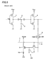
- Fig. 5 shows an example of a transmission circuit for transmitting image data Vd to a display panel.
- the reference numeral 1 indicates a transmitter circuit formed in an image signal processing LSI that amplifies and outputs image data Vd, and that is configured with a CMOS inverter.
- the reference numeral 2 indicates a transmission line connected to the transmitter circuit 1, and the reference numeral 3 a transmission line capacitance attached to the transmission line 2.
- the reference numeral 4 indicates a receiver circuit formed in a display panel side that amplifies the received image data Vd transmitted from the transmitter circuit 1 through the transmission line 3.
- the reference numeral 5 denotes a CMOS type transfer gate controlled by a switching signals (a horizontal scanning signal) SW, *SW (*SW is an inverted signal of SW).
- the CMOS type transfer gate 5 turns on and off according to the switching signals SW, *SW and transmits the image data Vd received by the receiver circuit 4 to a drain line 6 of the display panel.
- the reference numeral 7 indicates a gate line that receives a gate signal (a vertical scanning signal) from a gate driver (not shown in this figure)
- a pixel GS is formed near the point where the drain line 6 and the gate line 7 intersect. Although only one pixel GS is shown in Fig. 5, a plurality of pixels GS is formed in a matrix configuration on the display panel.
- the pixel GS performs switching according to the gate signal.
- the pixel GS has a pixel selection TFT8 (Thin Film Transistor) for writing the image data in the pixel GS, a driver TFT9, a self luminescent element 10 (for example, a LED element, an organic EL element, or an inorganic EL element) that emits light by the driving electric current fed from the driver TFT9, and a capacitor 11 for holding the image data written in the pixel GS for one horizontal period.
- TFT8 Thin Film Transistor
- This CMOS type signal transmission circuit is capable of making a display on the display panel based on the image data Vd that is processed by an image signal processing LSI and transmitted through high-speed transmission from the transmitter circuit 1 to the receiver circuit 4 in the display panel side through the transmission line 2.
- the CMOS type signal transmission circuit basically performed the transmission of signal by charging and discharging the transmission line capacitance 3 through the transmitter circuit 1.
- the gradation information for each image signal is a voltage information. Therefore, this causes problems including the radiation of EMI noise, the deterioration of the SN ratio of the voltage signal, the delayed transmission and the deterioration of image quality due to the varied skew among signals, when the signal frequency of the image data Vd is a high range, i.e., two-digit MHz frequencies. This makes the application of the transmitter circuit to the image equipment of private use very difficult.
- the invention provides an image data transmission circuit that includes a first transmission line and a second transmission line. At least part of the first and second transmission lines are substantially parallel to each other.
- the circuit also includes an electric current driving circuit that supplies a first current to the first transmission line based on image data and receives a second current from the second transmission line based on the image data. The first and second currents have substantially a same magnitude.
- the circuit also includes an electric current driven luminescent element driven by the electric current driving circuit to emit light.
- the invention also provides an image data display system that includes an image signal processing LSI including a pulse width modulation circuit generating a pulse width modulation signal having a modulated pulse width based on image data, and a first transmission line and a second transmission line. At least parts of the first and second transmission lines are substantially parallel to each other.
- the device also includes an electric current driving circuit that supplies a first current to the first transmission line based on the pulse width modulation signal and receives a second current from the second transmission line based on the pulse width modulation signal. The first and second currents have substantially a same magnitude.
- the device further includes an electric current driven luminescent element driven by the electric current driving circuit to emit light.
- the invention provide another image display system that includes an image signal processing LSI including a pulse width modulation circuit generating a pulse width modulation signal having a modulated pulse width based on image data, a display panel portion comprising an electric current driven luminescent element, and a first transmission line and a second transmission line that connect the image processing LSI and the display panel portion. At least parts of the first and second transmission lines are substantially parallel to each other.
- the device also includes an electric current driving circuit that supplies a first current to the first transmission line based on the pulse width modulation signal and receives a second current from the second transmission line based on the pulse width modulation signal.
- the first and second currents have substantially a same magnitude, and the electric current driven luminescent element is driven by the first current or the second current to emit light.
- image data is transmitted by having the first and second driving currents run through the first and second transmission lines based on the actual image data.
- noise induced by the driving currents is cancelled, thus minimizing radiation of EMI noise.
- the detrimental effects of such noise like deterioration of the SN ratio, delayed transmission due to differences in the parasitic capacitance of the transmission lines or the skew among signals can therefore be avoided.
- an improved transmission of image data with high frequency is achieved.
- Fig. 1 is a circuit diagram of the image data transmission circuit of this embodiment.
- the image data includes image data corresponding R (red), G (green), and B (blue).
- R red
- G green
- B blue
- the transmission circuits for the image data SG corresponding to G and the image data SB corresponding to B have the same configuration.
- the reference numeral 10 is a pulse width modulation circuit that modulates the image data SR with a certain bit number based on the gradation number into a pulse width modulation signal SRP with a modulated pulse width according to the size of the image data SR for a certain period.
- the reference numeral 30 is a driving electric current circuit that generates first and second driving currents I1, I2 corresponding to the pulse width modulation signal SRP.
- This circuit includes a pair of P-channel type MOS transistors M1, M2 and a pair of N-channel type MOS transistors M3, M4 making a differential transistor pair.
- a source voltage Vcc is applied to each source of the MOS transistors M1, M2.
- a gate of the MOS transistors M1 is connected to a drain of the MOS transistors M2 and a gate of the MOS transistors M2 is connected to a drain of the MOS transistors M1.
- the pulse width modulation signal SRP is applied to the gate of the N-channel type MOS transistor M3, and the inverted pulse width modulation signal *SRP inverted by an inverter 20 is applied to the gate of the N-channel type MOS transistor M4.
- a first transmission line 41 is connected to the drain of the N-channel type MOS transistor M4, and a second transmission line 42 is connected to the drain of the N-channel type MOS transistor M3.
- the first transmission line 41 and the second transmission line 42 are adjacent to each other and disposed extending from the transmitter side to the receiver side.
- the first and second driving electric currents I1 and I2 are supplied to the first and second transmission lines respectively.
- the first and second driving electric currents I1 and I2 have the same magnitude but have the opposite direction from each other.
- the drain of the P-channel type MOS transistor M5 is connected to the first transmission line 41 and the drain of the P-channel type MOS transistor M6 is connected to the second transmission line 42 on the receiver side.
- the source voltage Vcc is applied to the source of the P-channel type MOS transistor M5 and a delayed gate signal SELd that is a gate signal SEL1 of the P-channel type MOS transistor M1 delayed for a certain period by a delay circuit not shown in the figure is applied to the gate of the P-channel type MOS transistor M5.
- the source voltage Vcc is applied to the source of the P-channel type MOS transistor M6 and a delayed gate signal *SELd that is a gate signal *SEL1 of the P-channel type MOS transistor M2 delayed for a certain period by the delay circuit not shown in the figure is applied to the gate of the P-channel type MOS transistor M6.
- a CMOS transfer gate 51 that performs switching according to a switching signals SWO, *SW0 (*SW0 is an inverted signal of the SW0) and that supplies the first driving electric current I1 to a drain line 61 is connected to the first transmission line 41 on the receiver side.
- the switching signals SW0 and *SW0 are horizontal scanning signal and supplied from a horizontal driving circuit not shown in the figure.
- a pixel GS1 forming a pixel region of the display panel is disposed near the point where the drain line 61 and the gate line 60 intersect.
- the pixel GS1 has a pixel selection TFT 71 and an electric current driven luminescent element L1 (for example, a LED element, an organic EL element or an inorganic EL element).
- the gate line 60 is connected to the gate of the pixel selection TFT 71.
- a vertical scanning signal is supplied to the gate line 60 from a vertical scanning circuit not shown in the figure.
- the pixel selection TFT 71 performs switching according to the vertical scanning signal, supplying the first driving electric current I1 coming from the drain line 61 to the electric current driven luminescent element L1.
- CMOS transfer gate 52 that performs switching according to switching signals SW1, *SW1 (*SW1 is an inverted signal of the SW1) and that supplies the second driving electric current I2 to a drain line 62 is connected to the second transmission line 42 on the receiver side.
- the switching signals SW1 and *SW1 are also the horizontal scanning signal.
- the pixel GS2 part of the pixel region of the display panel, is disposed near the point where the drain line 62 and the gate line 60 intersect.
- the pixel GS2, like the pixel GS1, has the pixel selection TFT 72 and the electric current driven luminescent element L2 (for example, a LED element, an organic EL element or an inorganic EL element). Only a pair of GS1 and GS2 is shown in Fig. 1. However, the pixels with the same configuration are disposed in row direction as well as in the column direction in an actual display panel.
- the signal period tSR of the pulse width modulation signal SRP is determined.
- the pulse width of the pulse width modulation signal SRP is modulated in this period based on the size of the original image data SR.
- the N-channel type MOS transistor M3 of the electric current driving circuit 30 turns on when the pulse width modulation circuit SRP becomes high.
- the P-channel type MOS transistor M2 turns on when the gate signal *SEL1 of the P-channel type MOS transistor M2 becomes low.
- the P-channel type MOS transistor M1 turns off when the gate signal SEL1 of the P-channel type MOS transistor M1 becomes high.
- the delay gate signal SELd of the P-channel type MOS transistor M5 becomes high and the delay gate signal *SELd of the P-channel type MOS transistor M6 also becomes low.
- the P-channel type MOS transistor M5 turns off and the P-channel type MOS transistor M6 turns on.
- the first driving current I1 runs through the first transmission line 41 through the P-channel type MOS transistor M2 and the second driving current I2, which has the same magnitude as but the opposite direction from the first driving current I1, runs through the second transmission line 42 through the P-channel type MOS transistor M6.
- the second driving current I2 goes to the N-channel type MOS transistor M3 of the electric current driving circuit 30.
- the impedance of the MOS transistor as well as that of first and second transmission lines 41, 42 are adjusted to make the magnitude of the first and second driving currents I1 and I2 the same.
- the switching signal SW0 becomes high after the first and second driving currents I1, I2 are stabilized. Then, the CMOS transfer gate 51 turns on, feeding the first driving current I1 to the drain line 51 from the transmission line 41 through the CMOS transfer gate 51. The first driving current I1 is further fed to the electric current driven luminescent element L1 through the pixel selection TFT 71.
- a signal effective period ts during which the pulse width modulation signal SRP is effective to the luminescent display, is the duration starting from the time when the switching signal SW0 becomes high and finishing at the end of the signal duration tSR. The pulse width of the pulse width modulation signal SRP is modulated during the signal effective period ts.
- the first and second driving currents I1, I2 are fed to the electric current driven luminescent element L1, making the electric current driven luminescent element L1 emit the light according to the magnitude of the electric current.
- This magnitude is in proportion to the length of the pulse period of the pulse width modulation signal SRP, which corresponds to the period of the high level in this embodiment.
- the image data is transmitted from the transmitter side to the receiver side by letting the first and second driving currents I1, I 2 based on the image data run through the first and second transmission lines 41, 42 in this image data transmission circuit. Therefore, the noise with the driving currents I1 and I2 is canceled, preventing the radiation of EMI noise, the deterioration of the SN ratio, the delayed transmission due to the difference in the parasitic capacitance of the transmission lines, or the skew among signals, achieving the transmission of the image data with high frequency.
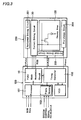
- the reference numeral 100 denotes the image signal processing LSI that has a processor 101 for performing a certain signal processing to the RGB image data supplied from outside, a frame memory for storing the processed image data, a timing controller 103 for generating various timing signals of the image signal processing LSI and various timing signals of the display panel 200, and a pulse width modulation circuit 10.
- the RGB image data supplied from outside is changed into the image data with a certain bit number according to the gradation number and stored in the frame memory 102 for each frame.
- the image data stored in the frame memory 102 is outputted to the pulse width modulation circuit 10 with a certain timing, generating the RGB pulse width modulation signal.
- the RGB pulse width modulation signal generated by the pulse width modulation circuit 10 is transmitted to the display panel 200.
- the display panel 200 has the electric current driving circuit 30 and the first and the second transmission lines 41, 42.
- the display panel also has a horizontal driving circuit 201, a vertical driving circuit 202, a display region 203, and a pre-charge circuit 204 of the drain line.
- This image data transmission system is suitable for a relatively large system with a transmission distance of above 10 cm of the image data and a transmission frequency of above 10MHz.
- the control of the transmission of the image signal at the side of the LSI 100, which is for signal processing, is extremely difficult when the transmission frequency is high because the signal transmission is significantly delayed and the electro magnetic radiation is increased. Therefore, the signal transmission from the image signal processing LSI 100 to the display panel 200 is performed through the pulse width modulation transmission, and the signal transmission within the side of the display panel is done by the electric currents with two opposite directions in this embodiment.
- FIG. 4 Another image data transmission system, which will be described below, can also be feasible depending on the transmission condition including the impedance of the transmission line. Another embodiment of the image data display system of this invention will be explained by referring to Fig. 4.
- the image data transmission system described above is also applied to this image data display system.
- This system has the pulse width modulation circuit 10 and the electric current driving circuit 30 of the transmitter side in the image signal processing LSI 100 and the P-channel type MOS transistors M5 and M6 of the receiver side in the display panel 200.
- the first and second transmission lines 41, 42 corresponding to RGB are formed between the image signal processing LSI 100 and the display panel 200.
- This image data display system is suitable for a small size display device including cell phone and DSC since the effect of the transmission distance and the frequency are relatively small.
- This system is especially effective if applied to the display device with an organic EL element because image signal processing LSI 100 can control the entire display region 203 of the display panel 200 with uniform electric current. Since it is not necessary to change the voltage for the electric current, the direct control of the display pixel TFT is possible with a relatively simple circuit configuration, achieving the better S/N ratio and the improved display with a high quality gradation with little electro magnetic radiation such as EMI.
Landscapes
- Engineering & Computer Science (AREA)
- Physics & Mathematics (AREA)
- Computer Hardware Design (AREA)
- Theoretical Computer Science (AREA)
- General Physics & Mathematics (AREA)
- Computer Networks & Wireless Communication (AREA)
- Signal Processing (AREA)
- Spectroscopy & Molecular Physics (AREA)
- Power Engineering (AREA)
- Chemical & Material Sciences (AREA)
- Crystallography & Structural Chemistry (AREA)
- Control Of Indicators Other Than Cathode Ray Tubes (AREA)
- Control Of El Displays (AREA)
- Electroluminescent Light Sources (AREA)
- Dc Digital Transmission (AREA)
Abstract
This invention enables the image data transmission with
high frequency without having the EMI noise or the deterioration
of SN ratio. The image data SR is inputted to the
electric current driving circuit (30) after it is modulated
into the pulse width modulation signal SRP by the pulse
width modulation circuit (10). The electric current driving
circuit (30) outputs the first and the second driving electric
current (I1, I2) to the transmission lines (41, 42)
based on the pulse width modulation signal SRP. The first
and the second driving electric currents (I1, I2) have the
same magnitude but the opposite directions. The pixels
(GS1, GS2) with the electric current driven luminescent
element (L1, L2) are driven by the first and second driving
electric currents (I1, I2).
Description
This invention relates to a transmission circuit that
transmits image data from one circuit to another and to a
display system with the transmission circuit.
CMOS type voltage signal transmission circuit is widely
used for transmitting image data. Fig. 5 shows an example
of a transmission circuit for transmitting image data Vd to
a display panel. The reference numeral 1 indicates a transmitter
circuit formed in an image signal processing LSI
that amplifies and outputs image data Vd, and that is configured
with a CMOS inverter. The reference numeral 2 indicates
a transmission line connected to the transmitter circuit
1, and the reference numeral 3 a transmission line capacitance
attached to the transmission line 2. The reference
numeral 4 indicates a receiver circuit formed in a
display panel side that amplifies the received image data
Vd transmitted from the transmitter circuit 1 through the
transmission line 3.
The reference numeral 5 denotes a CMOS type transfer gate
controlled by a switching signals (a horizontal scanning
signal) SW, *SW (*SW is an inverted signal of SW). The CMOS
type transfer gate 5 turns on and off according to the
switching signals SW, *SW and transmits the image data Vd
received by the receiver circuit 4 to a drain line 6 of the
display panel. The reference numeral 7 indicates a gate
line that receives a gate signal (a vertical scanning signal)
from a gate driver (not shown in this figure) A pixel
GS is formed near the point where the drain line 6 and the
gate line 7 intersect. Although only one pixel GS is shown
in Fig. 5, a plurality of pixels GS is formed in a matrix
configuration on the display panel.
The pixel GS performs switching according to the gate signal.
The pixel GS has a pixel selection TFT8 (Thin Film
Transistor) for writing the image data in the pixel GS, a
driver TFT9, a self luminescent element 10 (for example, a
LED element, an organic EL element, or an inorganic EL element)
that emits light by the driving electric current fed
from the driver TFT9, and a capacitor 11 for holding the
image data written in the pixel GS for one horizontal period.
This CMOS type signal transmission circuit is capable of
making a display on the display panel based on the image
data Vd that is processed by an image signal processing LSI
and transmitted through high-speed transmission from the
transmitter circuit 1 to the receiver circuit 4 in the display
panel side through the transmission line 2.
However, the CMOS type signal transmission circuit basically
performed the transmission of signal by charging and
discharging the transmission line capacitance 3 through the
transmitter circuit 1. The gradation information for each
image signal is a voltage information. Therefore, this
causes problems including the radiation of EMI noise, the
deterioration of the SN ratio of the voltage signal, the
delayed transmission and the deterioration of image quality
due to the varied skew among signals, when the signal frequency
of the image data Vd is a high range, i.e., two-digit
MHz frequencies. This makes the application of the
transmitter circuit to the image equipment of private use
very difficult.
It is an object of this invention to provide an improved
transmission circuit.
The solution according to the invention lies in the features
of the independent claims and preferably in those of
the dependent claims.
The invention provides an image data transmission circuit
that includes a first transmission line and a second transmission
line. At least part of the first and second transmission
lines are substantially parallel to each other. The
circuit also includes an electric current driving circuit
that supplies a first current to the first transmission
line based on image data and receives a second current from
the second transmission line based on the image data. The
first and second currents have substantially a same magnitude.
The circuit also includes an electric current driven
luminescent element driven by the electric current driving
circuit to emit light.
The invention also provides an image data display system
that includes an image signal processing LSI including a
pulse width modulation circuit generating a pulse width
modulation signal having a modulated pulse width based on
image data, and a first transmission line and a second
transmission line. At least parts of the first and second
transmission lines are substantially parallel to each
other. The device also includes an electric current driving
circuit that supplies a first current to the first transmission
line based on the pulse width modulation signal and
receives a second current from the second transmission line
based on the pulse width modulation signal. The first and
second currents have substantially a same magnitude. The
device further includes an electric current driven luminescent
element driven by the electric current driving circuit
to emit light.
The invention provide another image display system that includes
an image signal processing LSI including a pulse
width modulation circuit generating a pulse width modulation
signal having a modulated pulse width based on image
data, a display panel portion comprising an electric current
driven luminescent element, and a first transmission
line and a second transmission line that connect the image
processing LSI and the display panel portion. At least
parts of the first and second transmission lines are substantially
parallel to each other. The device also includes
an electric current driving circuit that supplies a first
current to the first transmission line based on the pulse
width modulation signal and receives a second current from
the second transmission line based on the pulse width modulation
signal. The first and second currents have substantially
a same magnitude, and the electric current driven
luminescent element is driven by the first current or the
second current to emit light.
According to the invention, image data is transmitted by
having the first and second driving currents run through
the first and second transmission lines based on the actual
image data. By using two lines, that are substantially parallel
to each other, noise induced by the driving currents
is cancelled, thus minimizing radiation of EMI noise. The
detrimental effects of such noise, like deterioration of
the SN ratio, delayed transmission due to differences in
the parasitic capacitance of the transmission lines or the
skew among signals can therefore be avoided. Thus, an improved
transmission of image data with high frequency is
achieved.
Next, an image data transmission circuit of an embodiment
of this invention will be explained by referring to figures.
Fig. 1 is a circuit diagram of the image data transmission
circuit of this embodiment. The image data includes
image data corresponding R (red), G (green), and B (blue).
However, only the transmission circuit for image data SR
corresponding to R will be explained for the sake of simplicity.
The transmission circuits for the image data SG
corresponding to G and the image data SB corresponding to B
have the same configuration.
The reference numeral 10 is a pulse width modulation circuit
that modulates the image data SR with a certain bit
number based on the gradation number into a pulse width
modulation signal SRP with a modulated pulse width according
to the size of the image data SR for a certain period.
The reference numeral 30 is a driving electric current circuit
that generates first and second driving currents I1,
I2 corresponding to the pulse width modulation signal SRP.
This circuit includes a pair of P-channel type MOS transistors
M1, M2 and a pair of N-channel type MOS transistors
M3, M4 making a differential transistor pair. A source
voltage Vcc is applied to each source of the MOS transistors
M1, M2. A gate of the MOS transistors M1 is connected
to a drain of the MOS transistors M2 and a gate of the MOS
transistors M2 is connected to a drain of the MOS transistors
M1.
The pulse width modulation signal SRP is applied to the
gate of the N-channel type MOS transistor M3, and the inverted
pulse width modulation signal *SRP inverted by an
inverter 20 is applied to the gate of the N-channel type
MOS transistor M4.
A first transmission line 41 is connected to the drain of
the N-channel type MOS transistor M4, and a second transmission
line 42 is connected to the drain of the N-channel
type MOS transistor M3. The first transmission line 41 and
the second transmission line 42 are adjacent to each other
and disposed extending from the transmitter side to the receiver
side. The first and second driving electric currents
I1 and I2 are supplied to the first and second transmission
lines respectively. The first and second driving electric
currents I1 and I2 have the same magnitude but have the opposite
direction from each other.
The drain of the P-channel type MOS transistor M5 is connected
to the first transmission line 41 and the drain of
the P-channel type MOS transistor M6 is connected to the
second transmission line 42 on the receiver side. The
source voltage Vcc is applied to the source of the P-channel
type MOS transistor M5 and a delayed gate signal
SELd that is a gate signal SEL1 of the P-channel type MOS
transistor M1 delayed for a certain period by a delay circuit
not shown in the figure is applied to the gate of the
P-channel type MOS transistor M5. Likewise, the source
voltage Vcc is applied to the source of the P-channel type
MOS transistor M6 and a delayed gate signal *SELd that is a
gate signal *SEL1 of the P-channel type MOS transistor M2
delayed for a certain period by the delay circuit not shown
in the figure is applied to the gate of the P-channel type
MOS transistor M6.
A CMOS transfer gate 51 that performs switching according
to a switching signals SWO, *SW0 (*SW0 is an inverted signal
of the SW0) and that supplies the first driving electric
current I1 to a drain line 61 is connected to the
first transmission line 41 on the receiver side. The
switching signals SW0 and *SW0 are horizontal scanning signal
and supplied from a horizontal driving circuit not
shown in the figure.
A pixel GS1 forming a pixel region of the display panel is
disposed near the point where the drain line 61 and the
gate line 60 intersect. The pixel GS1 has a pixel selection
TFT 71 and an electric current driven luminescent element
L1 (for example, a LED element, an organic EL element or an
inorganic EL element). The gate line 60 is connected to the
gate of the pixel selection TFT 71. A vertical scanning
signal is supplied to the gate line 60 from a vertical
scanning circuit not shown in the figure. The pixel selection
TFT 71performs switching according to the vertical
scanning signal, supplying the first driving electric current
I1 coming from the drain line 61 to the electric current
driven luminescent element L1.
Likewise, a CMOS transfer gate 52 that performs switching
according to switching signals SW1, *SW1 (*SW1 is an inverted
signal of the SW1) and that supplies the second
driving electric current I2 to a drain line 62 is connected
to the second transmission line 42 on the receiver side.
The switching signals SW1 and *SW1 are also the horizontal
scanning signal.
The pixel GS2, part of the pixel region of the display
panel, is disposed near the point where the drain line 62
and the gate line 60 intersect. The pixel GS2, like the
pixel GS1, has the pixel selection TFT 72 and the electric
current driven luminescent element L2 (for example, a LED
element, an organic EL element or an inorganic EL element).
Only a pair of GS1 and GS2 is shown in Fig. 1. However, the
pixels with the same configuration are disposed in row direction
as well as in the column direction in an actual
display panel.
Next, the operation of the image data transmission circuit
will be explained by referring to the operation timing
chart of Fig. 2.
The signal period tSR of the pulse width modulation signal
SRP is determined. The pulse width of the pulse width modulation
signal SRP is modulated in this period based on the
size of the original image data SR. The N-channel type MOS
transistor M3 of the electric current driving circuit 30
turns on when the pulse width modulation circuit SRP becomes
high. Then, after a little while, the P-channel type
MOS transistor M2 turns on when the gate signal *SEL1 of
the P-channel type MOS transistor M2 becomes low. Then, the
P-channel type MOS transistor M1 turns off when the gate
signal SEL1 of the P-channel type MOS transistor M1 becomes
high.
Then, the delay gate signal SELd of the P-channel type MOS
transistor M5 becomes high and the delay gate signal *SELd
of the P-channel type MOS transistor M6 also becomes low.
The P-channel type MOS transistor M5 turns off and the P-channel
type MOS transistor M6 turns on.
The first driving current I1 runs through the first transmission
line 41 through the P-channel type MOS transistor
M2 and the second driving current I2, which has the same
magnitude as but the opposite direction from the first
driving current I1, runs through the second transmission
line 42 through the P-channel type MOS transistor M6. The
second driving current I2 goes to the N-channel type MOS
transistor M3 of the electric current driving circuit 30.
The impedance of the MOS transistor as well as that of
first and second transmission lines 41, 42 are adjusted to
make the magnitude of the first and second driving currents
I1 and I2 the same.
The switching signal SW0 becomes high after the first and
second driving currents I1, I2 are stabilized. Then, the
CMOS transfer gate 51 turns on, feeding the first driving
current I1 to the drain line 51 from the transmission line
41 through the CMOS transfer gate 51. The first driving
current I1 is further fed to the electric current driven
luminescent element L1 through the pixel selection TFT 71.
A signal effective period ts, during which the pulse width
modulation signal SRP is effective to the luminescent display,
is the duration starting from the time when the
switching signal SW0 becomes high and finishing at the end
of the signal duration tSR. The pulse width of the pulse
width modulation signal SRP is modulated during the signal
effective period ts.
The first and second driving currents I1, I2 are fed to the
electric current driven luminescent element L1, making the
electric current driven luminescent element L1 emit the
light according to the magnitude of the electric current.
This magnitude is in proportion to the length of the pulse
period of the pulse width modulation signal SRP, which corresponds
to the period of the high level in this embodiment.
The image data is transmitted from the transmitter side to
the receiver side by letting the first and second driving
currents I1, I 2 based on the image data run through the
first and second transmission lines 41, 42 in this image
data transmission circuit. Therefore, the noise with the
driving currents I1 and I2 is canceled, preventing the radiation
of EMI noise, the deterioration of the SN ratio,
the delayed transmission due to the difference in the parasitic
capacitance of the transmission lines, or the skew
among signals, achieving the transmission of the image data
with high frequency.
Next, the image data display system of an embodiment of
this invention will be explained by referring to Fig. 3.
The image data transmission circuit mentioned above is used
in the image data display system. The reference numeral 100
denotes the image signal processing LSI that has a processor
101 for performing a certain signal processing to the
RGB image data supplied from outside, a frame memory for
storing the processed image data, a timing controller 103
for generating various timing signals of the image signal
processing LSI and various timing signals of the display
panel 200, and a pulse width modulation circuit 10.
The RGB image data supplied from outside is changed into
the image data with a certain bit number according to the
gradation number and stored in the frame memory 102 for
each frame. The image data stored in the frame memory 102
is outputted to the pulse width modulation circuit 10 with
a certain timing, generating the RGB pulse width modulation
signal.
The RGB pulse width modulation signal generated by the
pulse width modulation circuit 10 is transmitted to the
display panel 200. The display panel 200 has the electric
current driving circuit 30 and the first and the second
transmission lines 41, 42. The display panel also has a
horizontal driving circuit 201, a vertical driving circuit
202, a display region 203, and a pre-charge circuit 204 of
the drain line.
This image data transmission system is suitable for a relatively
large system with a transmission distance of above
10 cm of the image data and a transmission frequency of
above 10MHz. The control of the transmission of the image
signal at the side of the LSI 100, which is for signal
processing, is extremely difficult when the transmission
frequency is high because the signal transmission is significantly
delayed and the electro magnetic radiation is
increased. Therefore, the signal transmission from the image
signal processing LSI 100 to the display panel 200 is
performed through the pulse width modulation transmission,
and the signal transmission within the side of the display
panel is done by the electric currents with two opposite
directions in this embodiment.
Another image data transmission system, which will be described
below, can also be feasible depending on the transmission
condition including the impedance of the transmission
line. Another embodiment of the image data display
system of this invention will be explained by referring to
Fig. 4. The image data transmission system described above
is also applied to this image data display system. This
system has the pulse width modulation circuit 10 and the
electric current driving circuit 30 of the transmitter side
in the image signal processing LSI 100 and the P-channel
type MOS transistors M5 and M6 of the receiver side in the
display panel 200. The first and second transmission lines
41, 42 corresponding to RGB are formed between the image
signal processing LSI 100 and the display panel 200. This
image data display system is suitable for a small size display
device including cell phone and DSC since the effect
of the transmission distance and the frequency are relatively
small.
This system is especially effective if applied to the display
device with an organic EL element because image signal
processing LSI 100 can control the entire display region
203 of the display panel 200 with uniform electric current.
Since it is not necessary to change the voltage for the
electric current, the direct control of the display pixel
TFT is possible with a relatively simple circuit configuration,
achieving the better S/N ratio and the improved display
with a high quality gradation with little electro magnetic
radiation such as EMI.
Claims (9)
- An image data transmission circuit comprising:a first transmission line (41) and a second transmission line (42), at least parts of the first and second transmission lines (41, 42) being substantially parallel to each other;an electric current driving circuit (30) that supplies a first current to the first transmission line (41) based on image data and receives a second current from the second transmission line (42) based on the image data, the first and second currents having substantially a same magnitude; andan electric current driven luminescent element (L1, L2) driven by the electric current driving circuit (30) to emit light.
- The image data transmission circuit of claim 1, further comprising a pulse width modulation circuit (10) generating a pulse width modulation signal having a modulated pulse width for a predetermined period based on the image data and supplying the pulse width modulation signal to the electric current driving circuit (30) so that the electric current driving circuit (30) manipulates the first and second currents based on the modulated pulse width.
- The image data transmission circuit of claim 1 or 2, wherein the electric current driven luminescent element (L1, L2) comprises an LED element, an organic EL element or an inorganic EL element.
- An image data display system comprising:an image signal processing LSI (100) comprising a pulse width modulation circuit (10) generating a pulse width modulation signal having a modulated pulse width based on image data;a first transmission line (41) and a second transmission line (42), at least parts of the first and second transmission lines (41, 42) being substantially parallel to each other;an electric current driving circuit (30) that supplies a first current to the first transmission line (41) based on the pulse width modulation signal and receives a second current from the second transmission line (42) based on the pulse width modulation signal, the first and second currents having substantially a same magnitude; andan electric current driven luminescent element (L1, L2) driven by the electric current driving circuit to emit light.
- The image data display system of claim 4, further comprising a switching circuit (51, 52) supplying the first current or the second current to the electric current driven luminescent element (L1, L2) based on a switching signal.
- The image data display system of claim 4 or 5, wherein the electric current driven luminescent element (L1, L2) comprises an LED element or, organic EL element or an inorganic EL element.
- An image display system comprising:an image signal processing LSI (100) comprising a pulse width modulation circuit (10) generating a pulse width modulation signal having a modulated pulse width based on image data;a display panel portion (103) comprising an electric current driven luminescent element (L1, L2);a first transmission line (41) and a second transmission line (42) that connect the image processing LSI (100) and the display panel portion (103), at least parts of the first and second transmission lines (41, 42) being substantially parallel to each other; andan electric current driving circuit (30) that supplies a first current to the first transmission line (41) based on the pulse width modulation signal and receives a second current from the second transmission line (42) based on the pulse width modulation signal, the first and second currents having substantially a same magnitude and the electric current driven luminescent element (L1, L2) being driven by the first current or the second current to emit light.
- The image data display system of claim 7, wherein the display panel portion comprises a switching circuit (51, 52) supplying the first current or the second current to the electric current driven luminescent element (L1, L2) based on a switching signal.
- The image data display system of claim 7 or 8, wherein the electric current driven luminescent element (L1, L2) comprises an LED element, an organic EL element or an inorganic EL element.
Applications Claiming Priority (2)
| Application Number | Priority Date | Filing Date | Title |
|---|---|---|---|
| JP2004121205A JP2005301175A (en) | 2004-04-16 | 2004-04-16 | Video data transmission circuit and video data display system |
| JP2004121205 | 2004-04-16 |
Publications (1)
| Publication Number | Publication Date |
|---|---|
| EP1587215A1 true EP1587215A1 (en) | 2005-10-19 |
Family
ID=34935268
Family Applications (1)
| Application Number | Title | Priority Date | Filing Date |
|---|---|---|---|
| EP05008348A Withdrawn EP1587215A1 (en) | 2004-04-16 | 2005-04-18 | Image data transmission circuit and image data display system |
Country Status (6)
| Country | Link |
|---|---|
| US (1) | US20050243201A1 (en) |
| EP (1) | EP1587215A1 (en) |
| JP (1) | JP2005301175A (en) |
| KR (1) | KR20060045729A (en) |
| CN (1) | CN1694154A (en) |
| TW (1) | TW200604982A (en) |
Families Citing this family (3)
| Publication number | Priority date | Publication date | Assignee | Title |
|---|---|---|---|---|
| US12086498B2 (en) * | 2008-01-04 | 2024-09-10 | Nanolumens Acquisition, Inc. | Display system and methods |
| TWI521491B (en) * | 2014-04-07 | 2016-02-11 | 友達光電股份有限公司 | Data transmission system and operating method of display |
| KR20190010096A (en) * | 2017-07-21 | 2019-01-30 | 삼성전자주식회사 | Display apparatus and control method thereof |
Citations (3)
| Publication number | Priority date | Publication date | Assignee | Title |
|---|---|---|---|---|
| EP0933971A2 (en) * | 1998-01-30 | 1999-08-04 | Canon Kabushiki Kaisha | Light emitting element drive apparatus |
| US20020118716A1 (en) * | 2000-03-31 | 2002-08-29 | Seigo Furudate | Source follower circuit, laser driving apparatus, semiconductor laser apparatus, current-voltage convertion circuit, and light receiving circuit |
| US6510168B1 (en) * | 2000-03-06 | 2003-01-21 | Oki Electric Industry Co, Ltd. | Laser diode drive circuit |
Family Cites Families (1)
| Publication number | Priority date | Publication date | Assignee | Title |
|---|---|---|---|---|
| TW561445B (en) * | 2001-01-02 | 2003-11-11 | Chi Mei Optoelectronics Corp | OLED active driving system with current feedback |
-
2004
- 2004-04-16 JP JP2004121205A patent/JP2005301175A/en active Pending
-
2005
- 2005-04-04 TW TW094110696A patent/TW200604982A/en unknown
- 2005-04-13 CN CNA2005100645553A patent/CN1694154A/en active Pending
- 2005-04-14 US US11/105,579 patent/US20050243201A1/en not_active Abandoned
- 2005-04-15 KR KR1020050031229A patent/KR20060045729A/en not_active Ceased
- 2005-04-18 EP EP05008348A patent/EP1587215A1/en not_active Withdrawn
Patent Citations (3)
| Publication number | Priority date | Publication date | Assignee | Title |
|---|---|---|---|---|
| EP0933971A2 (en) * | 1998-01-30 | 1999-08-04 | Canon Kabushiki Kaisha | Light emitting element drive apparatus |
| US6510168B1 (en) * | 2000-03-06 | 2003-01-21 | Oki Electric Industry Co, Ltd. | Laser diode drive circuit |
| US20020118716A1 (en) * | 2000-03-31 | 2002-08-29 | Seigo Furudate | Source follower circuit, laser driving apparatus, semiconductor laser apparatus, current-voltage convertion circuit, and light receiving circuit |
Also Published As
| Publication number | Publication date |
|---|---|
| JP2005301175A (en) | 2005-10-27 |
| US20050243201A1 (en) | 2005-11-03 |
| CN1694154A (en) | 2005-11-09 |
| TW200604982A (en) | 2006-02-01 |
| KR20060045729A (en) | 2006-05-17 |
Similar Documents
| Publication | Publication Date | Title |
|---|---|---|
| TWI729671B (en) | Electronic display with hybrid in-pixel and external compensation | |
| TWI737214B (en) | Electronic devices with low refresh rate display pixels | |
| US8736589B2 (en) | Display device and driving method thereof | |
| US7561128B2 (en) | Organic electroluminescence display device | |
| US8514152B2 (en) | Display device with improved luminance uniformity among pixels and driving method thereof | |
| CN103165079B (en) | Organic light-emitting display device and method of operating thereof | |
| KR100734808B1 (en) | Pixel driving circuit with threshold voltage compensation | |
| CN100511366C (en) | Semiconductor device provided with matrix type current load driving circuits, and driving method thereof | |
| EP1221686A2 (en) | Driving circuit for an active matrix display with compensation of threshold voltage deviation | |
| US7075238B2 (en) | Organic light emitting display and display unit thereof | |
| KR102566579B1 (en) | Organic Light Emitting Diode display device | |
| US8284134B2 (en) | Display device and driving method thereof | |
| KR102575688B1 (en) | Display apparatus | |
| US20060125738A1 (en) | Light emitting display and method of driving the same | |
| KR20070056729A (en) | Organic light emitting diode display device and driving method thereof | |
| KR102563779B1 (en) | Organic light emitting diode display device | |
| US8310419B2 (en) | Display device and driving method thereof | |
| JP2016001266A (en) | Display circuit and display device | |
| US20150379935A1 (en) | Scan driver and display device using the same | |
| US9626910B2 (en) | Pixel driver circuit, display panel and driving method for the pixel driver circuit | |
| US10403203B2 (en) | Organic light emitting display device | |
| JP2005134880A (en) | Image display device, driving method thereof, and precharge voltage setting method | |
| CN112365842A (en) | Pixel circuit, driving method thereof and display device | |
| US7482997B2 (en) | Voltage/current driven active matrix organic electroluminescent pixel circuit and display device | |
| KR102628948B1 (en) | Gate driver, organic light emitting display apparatus and driving method thereof |
Legal Events
| Date | Code | Title | Description |
|---|---|---|---|
| PUAI | Public reference made under article 153(3) epc to a published international application that has entered the european phase |
Free format text: ORIGINAL CODE: 0009012 |
|
| AK | Designated contracting states |
Kind code of ref document: A1 Designated state(s): AT BE BG CH CY CZ DE DK EE ES FI FR GB GR HU IE IS IT LI LT LU MC NL PL PT RO SE SI SK TR |
|
| AX | Request for extension of the european patent |
Extension state: AL BA HR LV MK YU |
|
| 17P | Request for examination filed |
Effective date: 20060322 |
|
| AKX | Designation fees paid |
Designated state(s): DE FI FR GB NL |
|
| STAA | Information on the status of an ep patent application or granted ep patent |
Free format text: STATUS: THE APPLICATION HAS BEEN WITHDRAWN |
|
| 18W | Application withdrawn |
Effective date: 20070326 |