BACKGROUND OF THE INVENTION
1. Field of the Invention
This invention relates to an integrated circuit device
which is able to test connections of an internal circuit even if
it has a number of external pins.
2. Description of Related Art
Conventionally, particularly in logic LSI (Large Scale
Integrated Circuit), in order to simplify the circuit functions
test, it has been prevalent that the scantest circuit, which is
a dedicated circuit for the testing, is arranged in the LSI, and
the test is performed according to the scan path technique to check
if the combination circuits are properly operating.
This scantest circuit is configured with the scan path chain
in which the scan flip-flops are connected in series and operates
as a shift resistor. The scantest circuit comprises scan-in pins,
a scan-clock pin and scan-out pins. The scan-in pin is for
inputting scan-in signal that is the data for scantest (scantest
pattern) from outside or inside the LSI, the scan-clock pin is
for inputting the clock from outside the LSI for scan path test,
and the scan-out pin is for outputting the output data of the
scantest that is the result of the scantest.
In the scan path technique, during test mode (shift mode),
the scantest pattern for the test is supplied via the scan-in pins
(hereafter, referred to as "scan-in"), and the scan-clock for the
test is supplied to the clock pin. Then, the scantest pattern
is logic-computed by the combination circuit in the LSI to output,
from the scan-out pins, the result of the computation as a scantest
output data (hereafter, referred to as "scan-out") . By comparing
the outputted data with the predetermined expected value to check
whether or not they are equal, it is possible to see if the
combination circuit is properly operating. That is, if the
scanned-out outputted data matches the pre-calculated projection
value, it is determined that there is no defect in the combination
circuit. If not, it is determined that there is a manufacturing
defect. In this manner, by employing the scantest circuit, the
inside of the circuit can be separated as a combination circuit,
so that the testing can be simplified.
By the way, in such a test of LSI, if the number of the
external signals (external pins) of the LSI is greater than that
of the signals of the tester (test pins) for the testing, the new
tester having more test pins (hereafter, referred to as
"high-number-pins tester") is usually employed. But, employing
this high-number-pins tester requires installation of additional
new equipment. In addition, the high-number-pins tester is of
extremely expensive device.
As an example of such a method, Japanese Unexamined Patent
Application Publication No. 2003-57309 (hereafter, referred to
as "related art 1'') discloses that, on the LSI pad portion,
test-paths, each of which can be used as one of the nodes in a
logic circuit, are arranged between the input pad and the output
pad in a chip, so that the number of LSIs which can be
simultarieously measured is increased without reducing the failure
detection rate.
In another approach, a plurality of input pins are bound
onto the test board to virtually reduce the number of signals of
the LSI (hereafter, referred to as "related art 2") . Fig. 7 shows
the related art testing method for the integrated circuit device.
As shown in Fig.7, the LSI 201 has a number of the external pins,
then four external pins, namely four input pins 2021-2024 are
illustrated in Fig.7. These input pins 2021-2024 are connected
to input buffers 2031-2034 respectively. Four signal lines
2041-2044 which are to be inputted to the input pins 2021-2024 are
bound into one signal line 206 on the test board 205. The test
pin of the LSI tester is connected to this signal line 206 and
the test signal is supplied.
It has been discovered that there is a problem with the
related art 1 that a connection test of the internal circuit cannot
be performed by inputting the desired test signals from each input
pad, because the pad portion of the LSI is handled as one of the
nodes in the logic circuit. On the other hand, there is also a
problem with the related art 2, where one test signal is supplied
from the bound signal lines on the test board. That is, the signal
lines are externally bound into one line so that only the same
value can be supplied to the input pins, thus a satisfying function
test of the LSI would not be performed.
SUMMARY OF THE INVENTION
According to one aspect of the present invention, there is
provided an integrated circuit device which includes a plurality
of external pins and an internal circuit connected to the external
pins. The plurality of the external pins comprises a test pin
used during test mode, an unused external pin not used during the
test mode, and a control signal input pin receiving an unused pin
control signal which determines a configuration of the unused
external pin during the test mode.
According to the present invention, the unused pins, which
are not in use during the test mode, are controlled so that these
pins are configured in output mode or their voltages are fixed
to the power source level or the ground level by the unused pin
control signal, for example. This enables the connection test
in the LSI, even if the number of the external pins of the
integrated circuit device is greater than that of the pins of the
tester for testing the internal logic circuit and some of these
external pins are not connected to the tester.
BRIEF DESCRIPTION OF THE DRAWING
The objects, advantages and features of the present
invention will be more apparent from the following description
taken in conjunction with the accompanying drawings, in which:
DESCRIPTION OF THE PREFERRED EMBODIMENTS
The detailed explanations of the embodiments in accordance
with the present invention are provided as follows, by referring
to the drawings. With these embodiments, the present invention
is applied to the large LSI where the internal connections can
be tested even if the LSI has more pins than the tester to be used.
In the test of the large LSI, if the number of the external
pins (the number of the external signals of the LSI) for the use
of the scan path test of the internal logic circuit in the LSI
is greater than the number of the test pins (the number of the
signals for testing the LSI), some pins (the external signals)
of the LSI may not be connected to the tester during the test of
the LSI. Hereafter, in the specification, an external pin which
is not connected to the tester and not in use is referred to as
a floating pin.
In the case where part of the pins of the LSI are not
connected and are the floating pins, the following two problems
arise. That is;
Accordingly, in the first embodiment of the present
invention, in order to prevent the destruction of the input buffer
connected to the floating pin, the input pins and the
bidirectional pins in the input mode are forced into output mode
during the test mode. Then, the scan flip-flop SFF is connected
to each unused external pin, and the test signals are supplied
to the internal circuit using the scan chain consisting of these
flip-flops.
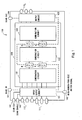
Fig. 1 is a schematic diagram illustrating the LSI according
to the present embodiment. As shown in Fig. 1, an LSI 110 comprises
external pins including bidirectional pins 111i, input pins 112j
and output pins 113k, an input/output circuit 121 connected to
the bidirectional pins 111i and the input pins 112j, an output
circuit 122 connected to the output pins 113k, and an internal
circuit 130 that is a logic circuit in the LSI.
The bidirectional pins 111i, the input pins 112j and the
output pins 113k are the external pins that are not used during
the test (i.e., floating pins) . In the internal circuit 130, the
scan path circuit consists of the internal scan flip-flops
SFF_A-SFF_D during the test mode so as to perform the scan path
test of the combination circuits 131-133.
The external pins include external pins 141-143, an
external pin 144 which outputs scan-out signal (SCAN OUT) that
is the result of the scan path test, a high-number-pins-test
switch signal pin 145 which is for inputting the
high-number-pins-test switch signal. The external pin 141 is a
pin for inputting the scan-in signal (SCANIN) that is the scan
path test signal for the scan path test of the internal circuit
130. The external pin 142 is a pin for inputting the scan-clock
signal (SCAN CLK) that is the clock signal for the scan path test.
The external pin 143 is a pin for inputting the scan-enable signal
(SCAN ENABLE) for selecting the output from the combination
circuit or the scan-in signal. The high-number-pins-test switch
signal pin 145 is a pin for inputting the high-number-pins-test
switch signal that functions as the unused pin control-signal for
determining the configuration of the floating pin. This signal
sets the unused bidirectional pins 111i and unused the input pins
112j to the output mode during the test mode.
In this LSI 110, the combination circuit 131 is tested
between the input/output circuit 121 and the SFF_A, SFF_B. The
combination circuit 132 is tested between the SFF_A, SFF_B and
the SFF_C, SFF_D. The combination circuit 133 is tested between
the output circuit 122 and the SFF_C, SFF_D.
Here, the LSI 110 in the present embodiment enables the test
to be performed without connecting all the external pins to the
tester. The shift resistor (scan path), which consists of scan
flip-flops connected to respective unused external pins, is
arranged in the input/output circuit 121 and the output circuit
122 between the external pins and the internal circuit 130.
Then, output buffers are provided, as required, to the
external pins which are to be the floating pins, and the floating
pins are set to the output mode by the high-number-pins-test
switch signals to prevent the signal input. The scan flip-flops
in the input/output circuit 121 and the output circuit 122 are
provided as a means for bypassing the unused pins and supplying
the desired test signals to the input of the internal circuit
connected to the floating pins. These scan flip-flops allow the
test of the internal circuit to be performed remaining the
external pins unused, that is, without inputting the test signals
from the external pins.
In further details, the output buffers are connected to the
input pins 112j of the unused pins and the output buffers are turned
on/off by the high-number-pins-test switch signal. Then, during
the test mode, the output buffers are turned on by the
high-number-pins-test switch signal to set to the output pins 112j
to the output mode. On the other hand, the output buffers of the
input/output buffers for the bidirectional pins 111i are
controlled based on the high-number-pins-test switch signal to
set the bidirectional pins 111i to the output mode. Here, the
high-number-pins-test switch signal pin 145 of the present
invention is connected to the common signal line for supplying
the high-number-pins-test switch signal to respective floating
pins, and controls the floating pins simultaneously during the
test mode.
It should be noted that, in Fig.1, pins except the pins
141-144 for inputting the test signals and the
high-number-pins-test switch signal pin 145 are explained as the
unused pins for the purpose of illustration. However, the
external pins which are not connected to the tester vary according
to the number of external pins, the circuit arrangement, the type
of the tester, and so on, and thus, not limited to the example
as shown in Fig.1. In addition, it is just required to set the
floating pins to the output mode by the high-number-pins-test
switch signal. Therefore, the floating pins may not be connected
to the scan flip-flops while the above explanation is provided
with the example in which respective floating pins are connected
to corresponding scan flip-flops. If the floating pins are not
connected to the scan flip-flops, the test of the floating pins
is performed with the tester connected to the floating pins after
the completion of the previous test. That is, the
high-number-pins-test switch signals may be supplied to the
external pins that are the potential unused pins.
Next, the detailed explanation is further provided
regarding the floating pins and the arrangement therewith in
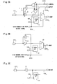
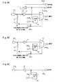
accordance with the present embodiment. Figs.2A-2C illustrate
the input/output portion to the external pins of the LSI according
to the present embodiment. Fig.2A shows the bidirectional pin
and the details of the input/output circuit portion thereof.
Fig.2B shows the input pin and the details of the input/output
circuit portion thereof. Fig. 2C shows the output pin and output
circuit portion thereof. As shown in Fig.2A, in the LSI 110 of
the present embodiment, the bidirectional pin 111i is connected
to the input/output circuit. The input/output circuit has an
input/output buffer 1, a scan flip-flop SFF 4 constituting a shift
resistor, a selection circuit 5, an OR circuit 6, and an EXOR
circuit (exclusive-OR circuit) 7.
The input/output buffer 1 comprises an input buffer 2 and
output buffer 3 connected to the bidirectional pin 111i. The SSF
4 is supplied with the output from the EXOR circuit 7, and stores
the data according to the timing of SCANCLK signal S105, and
outputs the stored data. The selection circuit 5 is supplied with
the output of the input buffer 2 and the output of the SFF 4, and
selects one of these outputs according to the
high-number-pins-test switch signal S101 and outputs it to the
internal circuit or the subsequent SFF as the input S1021. The
OR circuit 6 is supplied with the control signal (enable signal)
S103 which enables the output buffer 3 and the
high-number-pins-test switch signal S101, and outputs the logic
OR of these signals to set the bidirectional pin 111i to the output
mode during the test mode. The EXOR circuit 7 is supplied with
the control signal.S103 and the output signal 1041 from the
internal circuit in the LSI, and outputs the logic exclusive-OR.
While only the signal from the output of the internal circuit
(the output of the EXOR circuit 7) to the SFF 4 is shown in Fig.2A,
the SFF 4 receives the output from the preceding SFF and the output
of the EXOR circuit 7. It comprises a multiplexer supplied with
the output from the preceding SFF and the output of the EXOR circuit
7 and selecting one of these signals according to the scan-enable
signal. The SFF 4 further comprises a flip-flop supplied with
the signal selected by the multiplexer as Data input.
As shown in Fig. 2B, in the LSI 110 of the present embodiment,
the input pin 112j is connected to the input/output circuit. The
input/output circuit has an input buffer 11 connected to the input
pin 112j, an SFF 12 constituting the shift resistor with the SFF
4 and so on, a selection circuit 13, and an output buffer 14.
The SFF 12 is supplied with the output of the preceding SFF,
the output of the selection circuit 5 connected to the preceding
SFF or the scan-in signal as Data input. It reads the signal at
the timing according to the SCANCLK signal 1052 and supplies the
stored data to the selection circuit 13. The selection circuit
13 is supplied with the output of the input buffer 11 and the output
of the SFF 12, and selects one of these outputs according to the
high-number-pins-test switch signal S101 and outputs it as the
input S1022 for the internal circuit. The high-number-pins-test
switch signal S101 turns on and off the output buffer 14 to put
it into an enable state or a high impedance state. If the output
buffer 14 is in the enable state during the test mode, the input
pin 112j is in the output mode.
As shown in Fig.2C, in the LSI 110 of the present embodiment,
the output pin 113k is connected to the output circuit. The output
circuit has an output buffer 21 connected to the output pin 113k,
and an SFF 22 constituting the shift resistor with the SFF 4, the
SFF 12 and so on.
The SFF 22 consists of a flip-flop having the multiplexer
at the input, which selects and outputs one of the output signal
S1042 from the internal circuit and the output of the preceding
SFF according to the scan-enable signal. The SFF 22 reads it at
the timing according to the SCANCLK signal S1053, and outputs the
stored data.
It is possible to supply the high-number-pins-test switch
signal S101 to the OR circuit 6 and the selection circuit 5 and
the high-number-pins-test switch signal S101 to the output buffer
14 and the selection circuit 13, for example, from the
high-number-pins-test switch signal pin 145 shown in Fig.1 via
a common signal line. The high-number-pins-test switch signal
S101 may be set to "High" during the test mode and "Low" during
operation mode, for example.
The configuration of the unused pins belonging to the
bidirectional pin 111i is determined according to the
high-number-pins-test switch signal S101. That is, the
high-number-pins-test switch signal S101 turns on the output
buffer 3 of Fig.2A during the test mode to force the bidirectional
pins 111i into the output mode. It prevents noises from entering
the bidirectional pins 111i and the destruction of the input buffer
2 caused by the noises, even if the bidirectional pin 111i is not
connected to the tester, namely becomes the floating pin during
the test mode.
During the test mode, the output signal S1041 from the
internal circuit is supplied to the SFF 4 and the stored data is
supplied to the selection circuit 5 at the timing according to
the SCAKNCLK signal S1051. Then, the selection circuit 5 selects
the output of the SFF 4 according to the high-number-pins-test
switch signal S101 and supplied it to the internal circuit as the
input S1021. On the other hand, during operation mode, the
high-number-pins-test switch signal S101 is set to "Low". In this
case, in input mode, the control signal S103 becomes "Low", the
output buffer 3 is turned off, the input from the bidirectional
pin 111i is supplied to the selection circuit 5 via the input buffer
2, and the input from the bidirectional pin 111i is selected as
the input S1021 for the internal circuit. Also, in the output
mode during operation mode, the control signal S103 via the OR
circuit 6 turns on the output buffer 3, the output signal S1041
from the internal circuit is outputted from the bidirectional pin
111i via the output buffer 3.
As shown in Fig.2B, also at the input pin 112j, the
configuration of the unused pin is controlled using the
high-number-pins-test switch signal S101. That is, the output
buffer 14 is turned on by the high-number-pins-test switch signal
S101, and the input pin 112j is forced into the output mode.
Because of this, the input pin 112j does not become open,
preventing the destruction of the input buffer 12. On the other
hand, during operation mode, the high-number-pins-test switch
signal S101 is set to "Low", then the output buffer 14 is turned
off, and the input from the input pin 112j is selected at the
selection circuit 14 and supplied to the internal circuit as the
input 1022.
As shown in Fig.2C, in the output circuit connected to the
output pin 113k, the SFF 22 takes in the output signal S1042 from
the internal circuit during the test mode, then, the signal is
outputted from the scan-out pin 144 shown in Fig.1 or supplied
to the subsequent SFF. During operation mode, the output signal
S1042 from the internal circuit is outputted via the output pin
113k.
Here, the SFFs for the input/output circuit 121 and output
circuit 122 are the same as the SFF for the scan path circuit of
the internal circuit 130. Accordingly, each SFF comprises a
flip-flop and a multiplexer connected to the Data input of the
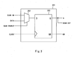
flip-flop. Fig.3 shows the arrangement of the typical scan
flip-flop SFF. As shown in Fig.3, the SFF 201 has a selection
circuit (multiplexer) 202 which selects one of the scan-in signal
and the data signal, and a D-flip-flop 202 which stores the data
of the multiplexer 203. The multiplexer 202 is supplied with the
scan-enable signal, and selects and outputs one of the scan-in
signal outputted from the scan-in pin or the preceding SFF and
the output data signal from the combination circuit. The
flip-flop 203 is supplied with the output of the multiplexer 202
as Data input, and reads and outputs the data at the timing
according to the scan-clock. The output Q can be scanned out and
detected during the test mode.
For arranging the scan path circuit, the flip-flop of the
corresponding portion is substituted by the scan flip-flop as
shown in Fig.3, and the scan path (scan chain) is configured by
connecting the scan flip-flops via a network.
There are two scan schemes, one is a full scan scheme and
the other is a partial scan scheme, any of which can be employed.
In the full scan scheme, all the flip-flops are substituted by
the scan flip-flops, while, in the partial scan scheme, a part
of the flip-flops are substituted by the scan flip-flops. When
the full scan scheme is employed, all the circuits can be handled
as the combination circuit, allowing the easier testing. When
the partial scan scheme is employed, the increase of the chip area
is reduced.
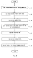
Next, the scan test method of the LSI 110 of the present
embodiment is explained. Fig.4 is a flowchart showing the
procedure of the test method. Fig.5 is timing chart showing the
logic levels of the high-number-pins-test switch signal S101, the
scan-enable signal and the scan-clock signal.
As shown in Fig.5, before the testing (period T1), the
high-number-pins-test switch signal S101 is "Low". When
starting the scantest, as shown in Figs.4 and 5, the
high-number-pins-test switch signal S101 is turned on ("High")
(step S1). This sets the bidirectional pin 111i and the input
pin 112j shown in Fig.2 to the output mode (step S2). The scan
path test hereafter is the same as the known arts. That is, the
scan-enable signal is turned on ("High") (step S3), and the
desired data (scan-in signal) is inputted from the'scan-in pin.
Then the SFF is set to a desired value by the shift resistor
operation (scan shift) according to the scan-clock signal (step
S4, period T2).
Subsequently, the scan-enable signal is turned off ("Low"),
the SFF reads the data (step S5, period T3), the scan-enable signal
is turned on ("High") (step S6), and the desired value of the SFF
is detected at the scan-out by another shift resistor operation
(step S7, period T4). When the test is completed, the
high-number-pins-test switch signal S101 is turned off ("Low")
again.
According to the present embodiment, by arranging the scan
chain with the SFF between the external pins and internal circuit
130, the scan-in signal can be supplied to the internal circuit
130 without routing the external pins, so that it is possible to
perform the same test as the case where the scan-in signal is
inputted from the external pins. Accordingly, even if there are
more external pins than the tester pins, there is no need for
preparing a new tester or binding the input signals into one, and
thus, it is possible to perform the connection test of the internal
circuit with the desired test signals. In this case, if the
floating pins during the test mode are the input pins or the
bidirectional pins, they are forced into the output mode by the
high-number-pins-test switch signal S101. Thus, even if these
pins are not connected to the tester, they do not become open,
so that noise cannot come in and destroy the input buffer connected
to the external pin.
Next, the second embodiment of the present invention is
explained. In the first embodiment above, the input pins and the
bidirectional pins in the input mode are forced into the output
mode by the high-number-pins-test switch signal, preventing
noises from coming into the floating pins and destroying the input
buffer connected thereto. On the other hand, in the present
embodiment, the floating pins are forced to be connected to the
power source or the ground according to the high-number-pins-test
switch signal. This prevents the destruction of the input buffer
similarly to the case of the first embodiment. Fig. 6 shows the
enlarged external pin portion according to the embodiment of the
present invention. In the embodiment shown in Fig. 6, the
constituent elements identical to those of the first embodiment
shown in Fig. 2 are assigned with the same reference symbols and
the detailed explanation thereof is omitted.
As shown in Fig.6A, the bidirectional pin 111i is connected
to the input/output circuit having the input buffer 1, the SFF
4 and the selection circuit 5 which selects and outputs one of
the input from the bidirectional pin 111i and the output from the
SFF 4. The bidirectional pin 111i is connected to a pull-down
circuitry. The pull-down circuitry comprises a pull-down resistor
8 connected to the bidirectional pin 111i and the switch 9 whose
one terminal is connected to the pull-down resistor 8 and the other
is grounded. During the test mode, the switch 9 is turned on by
the high-number-pins-test switch signal S101 to fix the voltage
level of the bidirectional pin 111i to the ground.
Also, as shown in the Fig. 6B, the input pin 112j is connected
to the input/output circuit having the input buffer 11, the SFF
12 and the selection circuit 5 which selects one of the inputs
thereof. The input pin 112j is connected to a pull-down circuitry.
The pull-down circuitry comprises a pull-down resistor 15
connected to the input pin 112j and the switch 16 whose one terminal
is connected to the pull-down resistor 15 and the other is grounded.
During the test mode, the switch 16, as well as the switch 9, is
turned on by the high-number-pins-test switch signal S101, to
fix the voltage level of the input pin 112j to the ground. The
arrangement of the output pin shown in Fig. 6C is the same as that
of the first embodiment shown in Fig.2C.
It should be noted that while the present embodiment
exemplifies the pull-down circuitry as a means for fixing the
voltage level of the external pins (the bidirectional pin and the
input pin), it is also possible to use the pull-up circuitry by
connecting a resistor and a switch in series between the external
pins and the power source and turning on/off the switch by the
high-number-pins-test switch signal S101.
According to the present embodiment, even if the tester pins
are fewer, the same test as the case of inputting the test signals
from all the external pins can be performed by arranging the
flip-flop between each input pin and the internal circuit and
employing the scantest. In addition, in the present embodiment
as well as the first embodiment shown in Fig.5, during the test
mode, the voltage levels of the bidirectional pin 111i and the
input pin 112j are grounded and stabilized by setting the
high-number-pins-test switch signal S101 to High. Thus, the
operation instability which would otherwise be caused by the open
pin is avoided, and destruction of the input buffer of the
input/output buffer is prevented.
It is apparent that the present invention is not limited
to the above embodiment and it may be modified and changed without
departing from the scope and spirit of the invention.