EP1582499A2 - Encapsulation wafer process - Google Patents
Encapsulation wafer process Download PDFInfo
- Publication number
- EP1582499A2 EP1582499A2 EP05075730A EP05075730A EP1582499A2 EP 1582499 A2 EP1582499 A2 EP 1582499A2 EP 05075730 A EP05075730 A EP 05075730A EP 05075730 A EP05075730 A EP 05075730A EP 1582499 A2 EP1582499 A2 EP 1582499A2
- Authority
- EP
- European Patent Office
- Prior art keywords
- wafer
- regions
- oxide
- oxide layer
- mask
- Prior art date
- Legal status (The legal status is an assumption and is not a legal conclusion. Google has not performed a legal analysis and makes no representation as to the accuracy of the status listed.)
- Withdrawn
Links
Images
Classifications
-
- B—PERFORMING OPERATIONS; TRANSPORTING
- B81—MICROSTRUCTURAL TECHNOLOGY
- B81C—PROCESSES OR APPARATUS SPECIALLY ADAPTED FOR THE MANUFACTURE OR TREATMENT OF MICROSTRUCTURAL DEVICES OR SYSTEMS
- B81C1/00—Manufacture or treatment of devices or systems in or on a substrate
- B81C1/00015—Manufacture or treatment of devices or systems in or on a substrate for manufacturing microsystems
- B81C1/00261—Processes for packaging MEMS devices
- B81C1/00333—Aspects relating to packaging of MEMS devices, not covered by groups B81C1/00269 - B81C1/00325
-
- B—PERFORMING OPERATIONS; TRANSPORTING
- B81—MICROSTRUCTURAL TECHNOLOGY
- B81C—PROCESSES OR APPARATUS SPECIALLY ADAPTED FOR THE MANUFACTURE OR TREATMENT OF MICROSTRUCTURAL DEVICES OR SYSTEMS
- B81C2203/00—Forming microstructural systems
- B81C2203/01—Packaging MEMS
- B81C2203/0118—Bonding a wafer on the substrate, i.e. where the cap consists of another wafer
Definitions
- the present invention generally relates to processes for fabricating semiconductor devices. More particularly, this invention relates to a process of producing encapsulation die through a process that simultaneously forms cavities and through-holes in a semiconductor wafer and provides both quality and cost improvements over current techniques.
- a microelectromechanical system (MEMS) device formed in or on a semiconductor die (referred to herein as a device die) is often capped by a semiconductor or glass die (referred to herein as a cap die), forming a package that defines a cavity within which the MEMS device, such as a suspended diaphragm or mass, is enclosed and protected.
- MEMS devices protected in this manner include accelerometers, rate sensors, actuators, pressure sensors, etc.
- MEMS devices For mass production, numerous MEMS devices are simultaneously fabricated in a device wafer that is bonded to an encapsulation (cap) wafer, after which the resulting wafer stack undergoes a dicing operation to singulate individual die packages from the wafers.
- the cavities are usually defined by recesses formed in the cap wafer by photolithographic/etch techniques.
- MEMS devices must be free to move to some degree, necessitating that the size and shape of the cavity within each package be adequate and consistently defined.
- current methods for processing cap wafers for MEMS devices are often plagued with yield loss and quality defects.
- cap wafers The difficulty in processing cap wafers revolves around the need to etch holes all the way through the cap wafer in order to provide access to bond pads on the device wafer.
- Existing processes utilize photolithographic/etch techniques to form the through-holes and recesses required by cap wafers.
- photolithography involves the use of light to effect the transfer of a pattern from a mask to a wafer, and using the pattern as a mask during etching of the wafer to define structural features, such as the holes and recesses in the cap wafer.
- Creating these through-holes using photolithographic/etch techniques requires processing both sides of the wafer and maintaining alignment of features on both sides.
- photolithographical patterning of the wafers requires individual handling of the wafers through several steps to create the pattern on the wafer. If both surfaces of the cap wafer are being patterned, the patterned side of the wafer must be placed against wafer handling fixtures in order to process the opposite surface of the wafer, which further aggravates the quality control problem. As each wafer is subjected to additional processing steps requiring individual handling of the wafer, the chances of creating a defect increase. For example, photolithographical masking defects or scratches during the processing of the cap wafer are translated into the cap wafer during the through wafer etch, resulting in defects that can lead to the loss of individual die and even the entire wafer.
- the present invention is directed to a method of processing a wafer, and particularly a cap wafer configured for mating with a device wafer in the production of a die package.
- the method makes use of a semiconductor wafer having first and second oxide layers on oppositely-disposed first and second surfaces, respectively, thereof.
- First and second masking layers are then deposited on the first and second oxide layers, respectively, after which the first and second masking layers are etched using photolithographic/etch techniques to define first and second mask patterns, respectively.
- the masking layers are patterned such that the first and second mask patterns expose regions of the first and second oxide layers, including first and second regions of the first oxide layer and first regions of the second oxide layer.
- the first mask pattern masks third and fourth regions of the first oxide layer and the second mask pattern masks second regions of the second oxide layer, with the fourth regions of the first oxide layer being aligned with the second regions of the second oxide layer.
- an oxide mask for a subsequent silicon etch is formed on the exposed first and second regions of the first oxide layer and the exposed first regions of the second oxide layer, but is prevented from forming on the third and fourth regions of the first oxide layer and the second regions of the second oxide layer as a result of the presence of the first and second masking layers.
- the first and second masking layers are then removed to expose the third and fourth regions of the first oxide layer and the second regions of the second oxide layer, after which the third and fourth regions of the first oxide layer and the second regions of the second oxide layer are removed to expose first, second and third regions, respectively, of the wafer.
- the first, second and third regions of the wafer are then etched, wherein etching of the first regions of the wafer produces recesses in the first surface of the wafer and etching of the second and third regions of the wafer produces through-holes in the wafer.
- the oxide mask is then removed to yield a cap wafer with multiple through-holes and recesses.
- the resulting feature etched in the cap wafer will have a smaller length and/or width dimension compared to the desired feature, and such a defect can be detected by an automated visual inspection.
- Figure 7 represents a MEMS device package 64 formed by bonding a device die 56 to a cap die 52.
- the device die 56 is schematically represented as carrying a micromachined element 58 that is enclosed within a cavity 60 between the die 52 and 56.
- the device die 56 is typically formed of a semiconductor material such as silicon, preferably monocrystallographic silicon, though it is foreseeable that other materials could be used.
- the cap die 52 is also preferably formed of a semiconductor material.
- the micromachined element 58 can be of any desired type, such as a proof mass, resonating structure, diaphragm or cantilever that relies on capacitive, piezoresistive and piezoelectric sensing elements to sense acceleration, motion, pressure, etc., all of which are known in the art.
- the micromachined element 58 is electrically interconnected to bond pads 62 on the device die 56, such as with conductive runners (not shown) in the form of aluminum metallization. Through the bond pads 62, the micromachined element 58 and its associated sensing elements can be electrically interconnected with appropriate signal conditioning circuitry (not shown).
- the cap die 52 is shown as having a recess 50 that defines the cavity 60 and a through-hole 48 that provides access to the bond pads 62 on the device die 56.
- the recess 50 and through-hole 48 are created by processing steps represented in Figures 1 through 6.
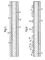
- a wafer 10 is schematically represented as having two opposite surfaces 12 and 14, each of which is covered with an oxide layer 16 and 18.
- the wafer 10 is preferably a [100] p-type silicon wafer that has been is polished on both surfaces 12 and 14.
- the sides of the wafer 10 at which the surfaces 12 and 14 are located will be referred to as the frontside and backside, though other terminology could be used.
- the wafer 10 is preferably sufficiently thick to permit handling while the lateral dimensions of the wafer 10 are generally large enough such that it can be subsequently diced into a number of individual chips, e.g., the cap die 52 in Figure 7.
- a suitable thickness for a wafer 10 having a diameter of about 125 millimeters is about 380 to about 625 micrometers.
- the oxide layers 16 and 18 are preferably thin oxide layers deposited or thermally grown in a conventional manner on the surfaces 12 and 14 of the wafer 10. Overlying the oxide layers 16 and 18 are films 20 and 22 of a material that will serve as a maskant for a subsequent oxidation step.
- a preferred material for the films 20 and 22 is silicon nitride (Si 3 N 4 ), with a suitable thickness being about 1500 to about 2000 Angstroms.
- Other suitable materials for the films 20 and 22 include those that have a low oxidation rate relative to silicon and are compatible with semiconductor processing.
- a suitable process for depositing the films 20 and 22 is low pressure chemical vapor deposition (LPCVD).
- the oxide layers 16 and 18 between the silicon wafer surfaces 12 and 14 and the films 20 and 22 serve as barriers that allow the films 20 and 22 to be removed without removing any of the wafer 10.
- suitable thicknesses for the oxide layers 16 and 18 are on the order of about 200 to about 750 Angstroms.
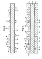
- Figure 2 the silicon nitride film 20 on the frontside of the wafer 10 has been patterned and etched
- Figure 3 shows the result of patterning and etching the silicon nitride film 22 on the backside of the wafer 10.
- the nitride films 20 and 22 are preferably etched using a dry etch. The etching operation produces openings 24, 26 and 38 in the nitride films 20 and 22 that expose underlying regions 32, 34 and 40, respectively, of the oxide layers 16 and 18.
- the remaining portions of the nitride films 20 and 22 define islands 28, 30 and 36 on the frontside and backside of the wafer 10.
- the islands 30 and 36 are aligned and correspond to the future locations of through-holes 48 in the wafer 10 ( Figure 5), and therefore the through-hole 48 in the cap die 52 of Figure 7.
- the islands 28 on the frontside of the wafer 10 correspond to the future locations of recesses 50 in the wafer 10 ( Figure 5), and therefore the recess 50 in the cap die 52 of Figure 7.
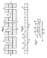
- the wafer 10 undergoes oxidation to grow a thick field oxide 42 ( Figure 4) on the regions 32, 34 and 40 of the oxide layers 16 and 18 exposed by the openings 24, 26 and 38 patterned and etched in the nitride films 20 and 22.
- the field oxide 42 forms a continuous matrix that surrounds each of the individual islands 28, 30 and 36 of the nitride films 20 and 22.
- the field oxide 42 will serve as an etch mask during etching of the through-holes 48 and recesses 50, and as such needs to be sufficiently thick to protect the wafer 10 during the etch process. Suitable thicknesses will depend on the etch rate of oxide using a particular wet or dry etch process. For example, a thickness of at least 5000 Angstroms is desirable if using the preferred wet chemical anisotropic etchant tetramethyl ammonium hydroxide (TMAH).
- TMAH wet chemical anisotropic etchant
- LOCOS local oxidation of silicon
- the islands 28, 30 and 36 of the nitride films 20 and 22 are removed, such as with the use of phosphoric acid (H 3 PO 4 ), so as not to damage the field oxide 42.
- Removal of the islands 28, 30 and 36 exposes underlying regions 44, 45 and 46 of the oxide layers 16 and 18 that coincide in size and shape to the islands 28, 30 and 36, respectively.
- the regions 45 and 46 are aligned and correspond to the future locations of the through-holes 48 in the wafer 10 ( Figure 5).
- the regions 44, 45 and 46 are etched, such as through the use of a BOE (buffered oxide etch) dip, to expose underlying surface regions of the wafer 10.
- BOE biuffered oxide etch
- the BOE dip removes some oxide from the surface of the field oxide 42 but not enough to destroy its usefulness as a mask.
- the exposed wafer surface regions are etched to yield the structure represented in Figure 5.
- the wafer etch is preferably performed with the wet chemical anisotropic etchant TMAH.
- TMAH wet chemical anisotropic etchant
- Figure 6 shows the result of stripping the field oxide 42 from both sides of the wafer 10, resulting in the wafer 10 comprising an array of cap die 52.
- Each cap die 52 comprises a through-hole 48, a recess 50, and a land 54 that completely surrounds the recess 50.
- the lands 54 subsequently serve as bonding surfaces for the cap wafer 10 when mated and bonded to a device wafer (not shown).
- the through-holes 48 can be aligned with bond pads (such as the bond pads 62 of Figure 7) or any other feature on the device wafer to which access is desired.
- the recesses 50 are aligned with regions of the device wafer on which elements are present that are desired to be encapsulated (such as the micromachined element 58 of Figure 7). Thereafter, individual device packages (such as the package 64 in Figure 7) can be sawn from the wafer stack produced by the wafer bonding operation. As known in the art, if the operation of the micromachined element 58 requires or benefits from operating in a vacuum, the cap wafer 10 can be bonded to the device wafer so that each cavity 60 defined by the recesses 50 forms a reference vacuum chamber.
- the above processing steps offer several advantages over prior practices in which photolithographic techniques are used to define the through-holes and recesses in cap wafers.
- One notable advantage is that this process moves all the single wafer patterning steps ahead of the step that forms the field oxide 42 used as the mask to define the through-holes 48 and recesses 50. As such, the field oxide 42 is formed and then used without handling every wafer in the cassette.
- Another notable advantage is that the process is "self healing" to the extent that defects that might occur during patterning and etching of the nitride films 20 and 22 will not become etch defects in the wafer 10.
- any region exposed by a defect in the nitride films 20 and 22 and not in the islands 28, 30, and 36, will be eliminated when the nitride is patterned, while any defects in the nitride films 20 and 22 within the islands 28, 30, and 36 will become oxidized during growth of the field oxide 42.
- the use of an anisotropic etchant such as TMAH will cause most oxide islands present in such defects to be undercut, such that the original defect in the nitride film 20 or 22 will not detrimentally effect the desired dimensions of the through-holes 48 and recesses 50.
- the process of this invention has the potential for dramatically improving the quality of cap wafers while also decreasing the manufacturing costs associated with producing these wafers.
Landscapes
- Engineering & Computer Science (AREA)
- Microelectronics & Electronic Packaging (AREA)
- Manufacturing & Machinery (AREA)
- Micromachines (AREA)
- Weting (AREA)
Abstract
Description
Claims (7)
- A method of processing a cap wafer (10) configured for mating with a device wafer in the production of a die package (64), the method comprising the steps of:providing a semiconductor wafer (10) having first and second oxide layers (16,18) on oppositely-disposed first and second surfaces (12,14), respectively, thereof;forming first and second masking layers (20,22) on the first and second oxide layers (16,18), respectively;etching the first and second masking layers (20,22) to define first and second mask patterns (28,30,36), respectively, the first and second mask patterns (28,30,36) exposing regions (32,34,40) of the first and second oxide layers (16,18), the exposed regions (32,34,40) comprising first and second exposed regions (32,34) of the first oxide layer (16) and first exposed regions (40) of the second oxide layer (18), the first mask pattern (28,30) masking third and fourth regions (44,45) of the first oxide layer (16) and the second mask pattern (36) masking second regions (46) of the second oxide layer (18), the fourth regions (45) of the first oxide layer (16) being aligned with the second regions (46) of the second oxide layer (18);forming an oxide mask (42) on the first and second exposed regions (32,34,40) of the first and second oxide layers (16,18), the first and second mask patterns (28,30,36) preventing the oxide mask (42) from forming on the third and fourth regions (44,45) of the first oxide layer (16) and the second regions (46) of the second oxide layer (18);removing the first and second mask patterns (28,30,36) to expose the third and fourth regions (44,45) of the first oxide layer (16) and the second regions (46) of the second oxide layer (18);removing the third and fourth regions (44,45) of the first oxide layer (16) and the second regions (46) of the second oxide layer (18) to expose first, second and third surface regions, respectively, of the wafer (10) between portions of the oxide mask (42);etching the first, second and third surface regions of the wafer (10), wherein etching of the first surface regions of the wafer (10) produces recesses (50) in the first surface (12) of the wafer (10) and etching of the second and third surface regions of the wafer (10) produces through-holes (48) in the wafer (10); and thenremoving the oxide mask (42) to yield a cap wafer (10) with multiple through-holes (48) and recesses (50).
- The method according to claim 1, characterized in that the first and second masking layers (20,22) are formed of silicon nitride.
- The method according to claim 1, characterized in that the wafer (10) is a silicon wafer (10), the first and second oxide layers (16,18) are silicon dioxide layers (16,18), and the oxide mask (42) is formed of silicon dioxide grown by oxidizing the first and second exposed regions (32,34) of the first oxide layer (16) and the second exposed region (40) of the second oxide layer (18).
- The method according to claim 1, further comprising the step of mating the cap wafer (10) with a device wafer so that the recesses (50) of the cap wafer (10) define cavities (60) enclosing micromachined elements (58) on the device wafer, bonding the cap wafer (10) to the device wafer to form a wafer stack, and then singulating die from the wafer stack to produce multiple device packages (64).
- The method according to claim 4, characterized in that as a result of the mating step the through-holes (48) provide access to bond pads (62) on the device wafer.
- The method according to claim 1, characterized in that the step of etching the first, second and third surface regions of the wafer (10) to produce the through-holes (48) and the recesses (50) is an anisotropic etch.
- The method according to claim 1, characterized in that a surface defect is present in at least one of the first and second mask patterns (28,30,36) prior to the step of forming the oxide mask (42), the step of forming the oxide mask (42) results in oxide forming in the defect, and the step of etching the first, second and third surface regions of the wafer (10) causes the oxide in the defect to be undercut so as not to effect the sizes and shapes of the through-holes (48) or recesses (50) formed in the first, second and third surface regions of the wafer (10).
Applications Claiming Priority (2)
| Application Number | Priority Date | Filing Date | Title |
|---|---|---|---|
| US708936 | 2004-04-01 | ||
| US10/708,936 US7118991B2 (en) | 2004-04-01 | 2004-04-01 | Encapsulation wafer process |
Publications (2)
| Publication Number | Publication Date |
|---|---|
| EP1582499A2 true EP1582499A2 (en) | 2005-10-05 |
| EP1582499A3 EP1582499A3 (en) | 2006-04-19 |
Family
ID=34886468
Family Applications (1)
| Application Number | Title | Priority Date | Filing Date |
|---|---|---|---|
| EP05075730A Withdrawn EP1582499A3 (en) | 2004-04-01 | 2005-03-29 | Encapsulation wafer process |
Country Status (2)
| Country | Link |
|---|---|
| US (1) | US7118991B2 (en) |
| EP (1) | EP1582499A3 (en) |
Cited By (2)
| Publication number | Priority date | Publication date | Assignee | Title |
|---|---|---|---|---|
| WO2010144051A1 (en) * | 2009-06-11 | 2010-12-16 | Agency For Science, Technology And Research | Microelectromechanical system (mems) device, method of operating the same, and method of forming the same |
| CN114195092A (en) * | 2021-11-30 | 2022-03-18 | 合肥工业大学 | A very small leak rate vacuum leak packaging method based on glass fusion bonding |
Families Citing this family (8)
| Publication number | Priority date | Publication date | Assignee | Title |
|---|---|---|---|---|
| TWI255503B (en) * | 2004-07-30 | 2006-05-21 | Touch Micro System Tech | Method of double-sided etching |
| US7564172B1 (en) * | 2005-08-03 | 2009-07-21 | Kolo Technologies, Inc. | Micro-electro-mechanical transducer having embedded springs |
| US7880565B2 (en) * | 2005-08-03 | 2011-02-01 | Kolo Technologies, Inc. | Micro-electro-mechanical transducer having a surface plate |
| US7767543B2 (en) * | 2005-09-06 | 2010-08-03 | Semiconductor Energy Laboratory Co., Ltd. | Method for manufacturing a micro-electro-mechanical device with a folded substrate |
| KR100953351B1 (en) | 2008-07-21 | 2010-04-20 | 앰코 테크놀로지 코리아 주식회사 | Semiconductor package and manufacturing method thereof |
| EP2848586A1 (en) | 2013-09-13 | 2015-03-18 | Teknologian Tutkimuskeskus VTT | Wafer level encapsulation structure and fabrication method thereof |
| US9969614B2 (en) | 2015-05-29 | 2018-05-15 | Taiwan Semiconductor Manufacturing Company, Ltd. | MEMS packages and methods of manufacture thereof |
| US10242967B2 (en) | 2017-05-16 | 2019-03-26 | Raytheon Company | Die encapsulation in oxide bonded wafer stack |
Family Cites Families (8)
| Publication number | Priority date | Publication date | Assignee | Title |
|---|---|---|---|---|
| GB1437112A (en) | 1973-09-07 | 1976-05-26 | Mullard Ltd | Semiconductor device manufacture |
| US5177661A (en) | 1989-01-13 | 1993-01-05 | Kopin Corporation | SOI diaphgram sensor |
| DE59508560D1 (en) | 1994-11-24 | 2000-08-17 | Siemens Ag | Capacitive pressure sensor |
| DE19803186C1 (en) * | 1998-01-28 | 1999-06-17 | Bosch Gmbh Robert | Structured wafer production used in micro-mechanical sensor structure manufacture, without need for wafer edge lacquering or doping |
| US6444138B1 (en) * | 1999-06-16 | 2002-09-03 | James E. Moon | Method of fabricating microelectromechanical and microfluidic devices |
| EP1203748B1 (en) | 2000-01-19 | 2007-05-09 | Mitsubishi Denki Kabushiki Kaisha | Microdevice and its production method |
| US6670538B2 (en) | 2001-01-05 | 2003-12-30 | Endevco Corporation | Thermal radiation sensor |
| US6845664B1 (en) * | 2002-10-03 | 2005-01-25 | The United States Of America As Represented By The Administrator Of National Aeronautics And Space Administration | MEMS direct chip attach packaging methodologies and apparatuses for harsh environments |
-
2004
- 2004-04-01 US US10/708,936 patent/US7118991B2/en not_active Expired - Fee Related
-
2005
- 2005-03-29 EP EP05075730A patent/EP1582499A3/en not_active Withdrawn
Cited By (3)
| Publication number | Priority date | Publication date | Assignee | Title |
|---|---|---|---|---|
| WO2010144051A1 (en) * | 2009-06-11 | 2010-12-16 | Agency For Science, Technology And Research | Microelectromechanical system (mems) device, method of operating the same, and method of forming the same |
| US8755106B2 (en) | 2009-06-11 | 2014-06-17 | Agency For Science, Technology And Research | Microelectromechanical system (MEMS) device, method of operating the same, and method of forming the same |
| CN114195092A (en) * | 2021-11-30 | 2022-03-18 | 合肥工业大学 | A very small leak rate vacuum leak packaging method based on glass fusion bonding |
Also Published As
| Publication number | Publication date |
|---|---|
| US20050227400A1 (en) | 2005-10-13 |
| EP1582499A3 (en) | 2006-04-19 |
| US7118991B2 (en) | 2006-10-10 |
Similar Documents
| Publication | Publication Date | Title |
|---|---|---|
| US5604160A (en) | Method for packaging semiconductor devices | |
| US5798283A (en) | Method for integrating microelectromechanical devices with electronic circuitry | |
| US7259436B2 (en) | Micromechanical component and corresponding production method | |
| US5963788A (en) | Method for integrating microelectromechanical devices with electronic circuitry | |
| US6428713B1 (en) | MEMS sensor structure and microfabrication process therefor | |
| US6448109B1 (en) | Wafer level method of capping multiple MEMS elements | |
| US7767484B2 (en) | Method for sealing and backside releasing of microelectromechanical systems | |
| US8952465B2 (en) | MEMS devices, packaged MEMS devices, and methods of manufacture thereof | |
| CN110040677A (en) | Micro- integration packaging MEMS sensor and its manufacturing method with machinery decoupling | |
| JPH0897439A (en) | One-chip integrated sensor | |
| US7026189B2 (en) | Wafer packaging and singulation method | |
| WO2007096636A1 (en) | Mems device | |
| US10894712B2 (en) | Optical electronics device | |
| US7118991B2 (en) | Encapsulation wafer process | |
| US6945110B2 (en) | Sensor design and process | |
| TWI418002B (en) | Chip package and method of manufacturing same | |
| TWI614816B (en) | Method for etching and dividing a lid wafer | |
| JPH11261079A (en) | Semiconductor device and method of manufacturing the same | |
| EP2848586A1 (en) | Wafer level encapsulation structure and fabrication method thereof | |
| CN116040579A (en) | Preparation method of MEMS device and MEMS wafer | |
| CN116946966A (en) | MEMS device and manufacturing method thereof | |
| US20070048888A1 (en) | Electrical contact for a MEMS device and method of making | |
| JP4288573B2 (en) | Semiconductor wafer chip forming method | |
| US7436076B2 (en) | Micromechanical component having an anodically bonded cap and a manufacturing method | |
| KR100817813B1 (en) | A method for fabricating a micro structures with multi differential gap on silicon substrate |
Legal Events
| Date | Code | Title | Description |
|---|---|---|---|
| PUAI | Public reference made under article 153(3) epc to a published international application that has entered the european phase |
Free format text: ORIGINAL CODE: 0009012 |
|
| AK | Designated contracting states |
Kind code of ref document: A2 Designated state(s): AT BE BG CH CY CZ DE DK EE ES FI FR GB GR HU IE IS IT LI LT LU MC NL PL PT RO SE SI SK TR |
|
| AX | Request for extension of the european patent |
Extension state: AL BA HR LV MK YU |
|
| PUAL | Search report despatched |
Free format text: ORIGINAL CODE: 0009013 |
|
| AK | Designated contracting states |
Kind code of ref document: A3 Designated state(s): AT BE BG CH CY CZ DE DK EE ES FI FR GB GR HU IE IS IT LI LT LU MC NL PL PT RO SE SI SK TR |
|
| AX | Request for extension of the european patent |
Extension state: AL BA HR LV MK YU |
|
| RIC1 | Information provided on ipc code assigned before grant |
Ipc: B81C 3/00 20060101ALI20060227BHEP Ipc: B81B 7/00 20060101ALI20060227BHEP Ipc: B81C 1/00 20060101AFI20050715BHEP |
|
| 17P | Request for examination filed |
Effective date: 20061019 |
|
| AKX | Designation fees paid |
Designated state(s): AT BE BG CH CY CZ DE DK EE ES FI FR GB GR HU IE IS IT LI LT LU MC NL PL PT RO SE SI SK TR |
|
| GRAP | Despatch of communication of intention to grant a patent |
Free format text: ORIGINAL CODE: EPIDOSNIGR1 |
|
| STAA | Information on the status of an ep patent application or granted ep patent |
Free format text: STATUS: THE APPLICATION IS DEEMED TO BE WITHDRAWN |
|
| 18D | Application deemed to be withdrawn |
Effective date: 20100915 |