EP1580906A2 - Dispersion compensating method and dispersion compensating apparatus - Google Patents
Dispersion compensating method and dispersion compensating apparatus Download PDFInfo
- Publication number
- EP1580906A2 EP1580906A2 EP04016111A EP04016111A EP1580906A2 EP 1580906 A2 EP1580906 A2 EP 1580906A2 EP 04016111 A EP04016111 A EP 04016111A EP 04016111 A EP04016111 A EP 04016111A EP 1580906 A2 EP1580906 A2 EP 1580906A2
- Authority
- EP
- European Patent Office
- Prior art keywords
- dispersion
- dispersion compensating
- amount
- compensating
- optical signal
- Prior art date
- Legal status (The legal status is an assumption and is not a legal conclusion. Google has not performed a legal analysis and makes no representation as to the accuracy of the status listed.)
- Granted
Links
Images


Classifications
-
- H—ELECTRICITY
- H04—ELECTRIC COMMUNICATION TECHNIQUE
- H04B—TRANSMISSION
- H04B10/00—Transmission systems employing electromagnetic waves other than radio-waves, e.g. infrared, visible or ultraviolet light, or employing corpuscular radiation, e.g. quantum communication
- H04B10/25—Arrangements specific to fibre transmission
- H04B10/2507—Arrangements specific to fibre transmission for the reduction or elimination of distortion or dispersion
- H04B10/2513—Arrangements specific to fibre transmission for the reduction or elimination of distortion or dispersion due to chromatic dispersion
- H04B10/25133—Arrangements specific to fibre transmission for the reduction or elimination of distortion or dispersion due to chromatic dispersion including a lumped electrical or optical dispersion compensator
-
- G—PHYSICS
- G02—OPTICS
- G02B—OPTICAL ELEMENTS, SYSTEMS OR APPARATUS
- G02B6/00—Light guides; Structural details of arrangements comprising light guides and other optical elements, e.g. couplings
- G02B6/24—Coupling light guides
- G02B6/26—Optical coupling means
- G02B6/28—Optical coupling means having data bus means, i.e. plural waveguides interconnected and providing an inherently bidirectional system by mixing and splitting signals
- G02B6/293—Optical coupling means having data bus means, i.e. plural waveguides interconnected and providing an inherently bidirectional system by mixing and splitting signals with wavelength selective means
- G02B6/29379—Optical coupling means having data bus means, i.e. plural waveguides interconnected and providing an inherently bidirectional system by mixing and splitting signals with wavelength selective means characterised by the function or use of the complete device
- G02B6/29392—Controlling dispersion
- G02B6/29394—Compensating wavelength dispersion
Definitions
- the present invention relates to a dispersion compensating method and a dispersion compensating apparatus, and, in particular, to a dispersion compensating method and a dispersion compensating apparatus for automatically compensating wavelength dispersion occurring in an optical fiber in a wavelength division multiplexing transmission system.
- a method in which dispersion compensation is performed for each wavelength requires the costs greatly higher than those required for the second method in which dispersion compensation is performed for all the wavelengths in a lump.
- dispersion slope in a transmission line depends on each particular optical fiber transmission line, it is not possible to completely compensate transmission line dispersion for all the wavelengths in the second method of performing dispersion compensation in a lump of all the wavelengths.
- a method of dividing a target wavelength band and performing dispersion compensation for each of the division wavelength bands exists.
- a dispersion compensator may be used there is such that an optical fiber such as a dispersion compensated fiber (DCF) as a typical example is cut for a length according to a dispersion amount, and is disposed according to a transmission line dispersion amount for each repeating section, so as to be used for the dispersion compensation.
- DCF dispersion compensated fiber
- variable dispersion compensator In contrast thereto, recently, a variable dispersion compensator has been put into practical use, and, it is expected that such an apparatus will spread sharply. It is known that, in order to control the variable compensator, an optimum dispersion amount is set with the use of code error information such as error correction amount as disclosed by Japanese Laid-open Patent Application No. 2002-208892.
- Japanese Laid-open Patent Application No. 2003-46443 discloses an art of detecting a duty ratio of an optical signal, and controlling a dispersion compensation amount in the variable compensator based on the duty ratio.
- Japanese Laid-open Patent Application No. 2000-244394 discloses an art of detecting maintainability in data transmitted, generating an electric feedback signal for controlling a current applied to a grating, and determining dispersion in the grating.
- the dispersion compensating amount should be controlled in a case where the transmission line dispersion fluctuates due to influence of ambient temperature or such.
- a direction of correction i.e., a direction in which the code error amount decreases
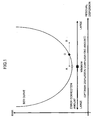
- the optimization is performed in such a manner in which, the dispersion compensating amount is changed in a fixed range to a residual dispersion amount A or B from a current residual dispersion amount O, and thus, a point at which BER (bit error rate) becomes minimum is sought.
- BER bit error rate
- the present invention has been devised in consideration of the above-mentioned problems, and, an object of the present invention is to provide a dispersion compensating method and a dispersion compensating apparatus by which it is possible to determine a direction of increasing or decreasing the dispersion compensating amount without a need of a possibility of actually increasing the BER.
- a dispersion compensating method for compensating wavelength dispersion occurring in an optical transmission line includes the steps of: a) performing dispersion compensation by causing an optical signal, supplied from the transmission line, to pass through a variable dispersion compensator; and b) controlling a dispersion compensating amount in the variable dispersion compensator according to code error information for a type of code in a received data signal obtained from receiving the optical signal having undergone the dispersion compensation.
- a dispersion compensating method for compensating wavelength dispersion occurring in an optical transmission line includes the steps of: a) performing dispersion compensation by causing an optical signal, supplied from the transmission line, to pass through a variable dispersion compensator; and b) controlling a dispersion compensating amount in the variable dispersion compensator according to code error information comprising a code error rate and the number of errors for each type of code in a received data signal obtained from receiving the optical signal having undergone the dispersion compensation.
- a dispersion compensating apparatus for compensating wavelength dispersion occurring in an optical transmission line, includes: a variable dispersion compensating part performing dispersion compensation by causing an optical signal, supplied from the transmission line, to pass through a variable dispersion compensator; a light receiving part receiving an optical signal having undergone dispersion compensation and obtaining a received data signal therefrom; an error correcting part performing error correction on the received data signal obtained by the light receiving part and obtaining code error information for a type of corrected code; and a control part controlling a dispersion compensating amount in the variable dispersion compensating part according to the code error information obtained by the error correcting part.
- control part may control the dispersion compensating amount in the variable dispersion compensating part according to the code error information and an S/N ratio of the optical signal in the light receiving part.
- the code error information may include the number of corrected bits from 0 to 1 and the number of corrected bits from 1 to 0; and the control part may increase or decrease the dispersion compensating amount according to a correction ratio from 0 to 1, which is a ratio of the number of corrected bits from 0 to 1 with respect to the sum total of the number of corrected bits from 0 to 1 and the number of corrected bits from 1 to 0.
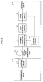
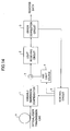
- FIG. 4 shows a block diagram of a configuration of a dispersion compensating apparatus in a first embodiment of the present invention.
- the dispersion compensating apparatus includes a variable dispersion compensator 1, a light receiving circuit 2, an error correction circuit 3 and a control circuit 4.
- An optical signal supplied to the variable dispersion compensator 1 through an optical fiber transmission line 5 is an optical signal at a high bit rate of 40 Gb/s or such for example, in which waveform degradation may occur due to dispersion characteristics of the optical fiber transmission line 5.
- the variable dispersion compensator 1 is a well-known optical device which has a function of variably compensating wavelength dispersion which input light has. Specifically, for example, a VIPA (virtually imaged phased array) device, an optical device employing a FBG (fiber Bragg grating), or such may be applied thereto. This variable dispersion compensator 1 performs polarization dispersion compensation simultaneously as well as wavelength dispersion compensation simultaneously.
- the light receiving circuit 2 receives the optical signal output from the variable dispersion compensator 1, converts it into an electric signal, performs well-known signal reception processing such as clock reproduction, data discrimination and so forth, and outputs a received data signal indicating the processing result, to the error correction circuit 3.
- the error correction circuit 3 performs error correction with the use of error correction code included in the received data signal output from the light receiving circuit 2, obtains a code error rate such as BER (bit error rate) and error correcting contents, and provides the thus-obtained information to the control circuit 4 as code error information.
- a code error rate such as BER (bit error rate)
- error correcting contents such as BER (bit error rate)
- BER bit error rate
- a well-known manner may be applied, such as a manner of determining the code error by performing parity check on the received data signal, a manner of utilizing a B1 or a B2 byte in the signal conforming to the SONET or SDH standard, for example.
- an error correction amount and error correction contents detected during the error correction processing are provided to the control circuit 4 as the code correction information.
- the control circuit 4 performs automatic control of a wavelength dispersion compensating amount in the variable dispersion compensator 1 based on the code error information such as the code error rate and the error correction contents provided by the error correction circuit 3, such as to reduce the code error included in the optical signal output from the variable dispersion compensator 1.
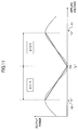
- a correction ratio curve IV representing a ratio (called 'correction ratio from 0 to 1') of the number of corrected bits from 0 to 1 with respect to the sum total of the number of corrected bits from 0 to 1 and the number of corrected bits from 1 to 0 has characteristics such that the correction ratio from 0 to 1 has a value of approximately 50 % at the point of the optimum dispersion compensating amount (corresponding to the point of the minimum BER), decreases as the residual dispersion becomes smaller and increases as the residual dispersion becomes larger.
- control circuit 4 obtains the correction ratio from 0 to 1 based on the number of corrected bits from 0 to 1 and the number of corrected bits from 1 to 0, automatically controls the dispersion compensating amount in the variable dispersion compensator 1 in a direction such that the correction ratio from 0 to 1 may approach 50 %, and thus, BER may become minimum.
- the automatic control of the variable dispersion compensator 1 is performed based on the correction ratio from 0 to 1, i.e., a/(a + b), where 'a' denotes the number of corrected bits from 0 to 1, and 'b' denotes the number of corrected bits from 1 to 0.
- the code error information provided by the error correction circuit 3 may include instead the code error rate and the number of erroneous bits of 0 and the number of erroneous bits of 1.
- the code error rate (the number of errors occurring per unit time) can be easily calculated from this number by dividing the number with the relevant time interval.
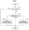
- FIG. 6 shows a flow chart of dispersion compensating control processing executed by the control part 4 according to the first embodiment of the present invention. This processing is repeated every predetermined time interval.
- Step S10 it is determined whether or not the BER is the minimum value. When the BER is the minimum value, the current processing is finished. On the other hand, when the BER is not the minimum value, Step S12 is performed. In Step S12, it is determined whether the above-mentioned correction ratio from 0 to 1b is less than 50 %, is just 50 % or is more than 50 %.
- the dispersion compensating amount in the variable dispersion compensator 1 is controlled in such a direction that the residual dispersion amount may increase, in Step S14.
- the current processing is finished.
- the dispersion compensating amount in the variable dispersion compensator 1 is controlled in such a direction that the residual dispersion amount may decrease, in Step S16.
- Step S10 it is also possible to determine whether or not the BER does not exceed a predetermined threshold. In this case, when the BER is less than the predetermined threshold, the current processing is finished, while, when the BER exceeds the threshold, the processing is proceeded with from Step S12. This alternative may also be applied to any other embodiment described below.
- the first embodiment of the present invention it is possible to determine, according to the correction ratio from 0 to 1, whether the dispersion compensation amount should be increased or decreased in response to deviation in the residual dispersion amount from the optimum amount. Thus, it is possible to avoid taking a risk of increasing in the BER in the dispersion compensating control processing.
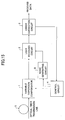
- FIG. 7 shows a block diagram of a dispersion compensating apparatus according to a second embodiment of the present invention.
- This embodiment is different from the embodiment shown in FIG. 4 in that OSNR (optical signal noise ratio) obtained in the optical receiving circuit 2 is supplied to the control circuit 4, which automatically controls the dispersion compensating amount in the variable dispersion compensator 1 according to the BER, the OSNR and the correction ratio from 0 to 1.
- OSNR optical signal noise ratio
- FIG. 8 shows a flow chart of dispersion compensating control processing executed by the control part 4 according to the second embodiment of the present invention. This processing is repeated every predetermined time interval.
- Step S10 it is determined whether or not the BER is the minimum value. When the BER is the minimum value, the current processing is finished. On the other hand, when the BER is not the minimum value, Step S11 is performed.
- Step S11 it is determined whether or not the OSNR given is degraded from one given in the preceding processing. When the OSNR is degraded (Yes in Step S11), the current processing is finished. On the other hand, when the OSNR is not degraded (No in Step S11), Step S12 is performed.
- Step S12 it is determined whether the correction ratio from 0 to 1 is less than 50 %, is just 50 % or is more than 50 %.
- the dispersion compensating amount in the variable dispersion compensator 1 is controlled in such a direction that the residual dispersion amount may increase, in Step S14.
- the current processing is finished.
- the dispersion compensating amount in the variable dispersion compensator 1 is controlled in such a direction that the residual dispersion amount may decrease, in Step S16.
- the dispersion compensating control processing is stopped when the OSNR is degraded. Therefore, it is possible to avoid unnecessary dispersion compensating control in such a case where the OSNR temporarily changes and soon returns to the original state.
- control of the dispersion compensating amount can be retrained in a case of degradation of the BER based on temporary degradation of the OSNR.
- FIG. 9 shows a block diagram of an optical transmission system in an embodiment of the present invention. As shown, an optical signal transmitted from an optical transmission apparatus 10 is transmitted to a light receiving apparatus 30 via an optical fiber transmission line 20.
- the optical transmission apparatus 10 includes a chirping generation circuit 11 giving chirping to an optical transmission signal to be transmitted. Further, to the optical transmission signal, error correction code is also given.
- the optical fiber transmission line 20 provides wavelength dispersion to an optical signal transmitted thereby according to a type, a length or such of the optical fiber itself. In the optical fiber transmission line 20, an optical repeater, not shown, may be provided.
- FIG. 10 shows a block diagram of the above-mentioned chirping generation circuit 11 in one embodiment.
- Chirp setting shown means to change a frequency in a laser diode 44 by selecting an operation point in a driving circuit 43 in an external modulator 45 in the optical transmission apparatus 10 as a result of an electric current injected to a laser diode 44 being controlled thereby.
- the above-mentioned selection of the operation point is commonly expressed by a ⁇ parameter having the value of +1 or -1.
- a transmission signal is supplied directly to, or is supplied, after being inverted by a NOT circuit 41, to a selector 42.
- the drive circuit 43 drives the external modulator 45 which modulates light output by the laser diode 44 with the thus-supplied transmission signal.
- the modulation driving is performed such that the reference potential Vth shown in FIG. 11 is treated as a low level (0) while a potential V2 lower than the reference potential Vth is treated as a high level (1).
- the optical receiving apparatus 30 employs the above-described dispersion compensating apparatus shown in FIG. 4. Which direction the residual desperation amount should be changed for the purpose of causing the correction ratio form 0 to 1 to approach 50 % is determined from the chirp setting in the optical transmission apparatus 10.
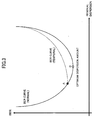
- a correction ratio curve IVa for the correction ratio from 0 to 1 is such that, approximately 50 % is obtained at the optimum dispersion compensating amount; the value decreases therefrom as the residual dispersion becomes smaller; and the value increases therefrom as the residual dispersion become larger.
- a correction ratio curve IVb for the correction ratio from 0 to 1 is such that, approximately 50 % is obtained at the optimum dispersion compensating amount; the value increases therefrom as the residual dispersion becomes smaller; and the value decreases therefrom as the residual dispersion become larger.
- the dispersion compensating amount in the variable dispersion compensator 1 is controlled in such a direction that the residual dispersion amount may increase when the correction ratio from 0 to 1 is less than 50 %, while the dispersion compensating amount in the variable dispersion compensator 1 is controlled in such a direction that the residual dispersion amount may decrease when the correction ratio from 0 to 1 is more than 50 %.
- the dispersion compensating amount in the variable dispersion compensator 1 is controlled in such a direction that the residual dispersion amount may decrease when the correction ratio from 0 to 1 is less than 50 %, while the dispersion compensating amount in the variable dispersion compensator 1 is controlled in such a direction that the residual dispersion amount may increase when the correction ratio from 0 to 1 is more than 50 %.
- the time required for optimizing the residual dispersion amount can be reduced by intentionally increasing the number of error corrections with the use of a noise adding part provided.
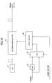
- FIG. 14 shows a block diagram of a depression compensating apparatus according to a third embodiment of the present invention.
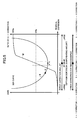
- the third embodiment is different from the embodiment shown in FIG. 4 in that an ASE light source 6 is provided. Only in a case where the BER is less than the above-mentioned threshold 'b1' supplied by the error correction circuit 3 as a code error rate, the ASE light source 6 is operated, and thereby, ASE (amplified spontaneous emission) light is generated thereby. The ASE light is then mixed by a multiplexer 7 to an optical signal output from the variable dispersion compensator 1.
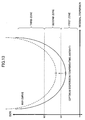
- the OSNR is degraded, and, thereby, the BER curve is degraded into a BER curve represented by a broken line in FIG. 13 in which the BER at the optimum compensating amount is in a second zone, which is more than 'b1' but less than 'b2'.
- the second zone is such that the number of error corrected bits is large to a certain extent, but, is within a range in which error correction can be performed.
- FIG. 15 shows a block diagram of a dispersion compensating apparatus according to a variant embodiment of the third embodiment of the present invention.
- a noise generating circuit 8 is provided instead of the ASE light source 6. Only in a case where the BER is less than the above-mentioned threshold 'b1' supplied by the error correction circuit 3 as a code error rate, the noise generating circuit 8 is operated, and thereby, electrical white noise is generated thereby. The white noise is then supplied to the light receiving circuit 2, is mixed there to a received signal which has been already converted into an electrical signal there.
- the BER curve is degraded into a BER curve represented by a broken line in FIG. 13 in which the BER at the optimum compensating amount is in a second zone, which is more than b1 and less than b2.
- the second zone is such that the number of error corrected bits is large to a certain extent, but is within a range in which error correction can be performed.
- FIG. 16 shows a block diagram of a wavelength division multiplexing transmission system in one embodiment of the present invention.
- a wavelength multiplexing transmission apparatus 50 at a transmission end includes transmitters 51 0 through 51n, a wavelength multiplexing part 52 and a transmission optical amplifier 53.
- the transmitter 51 0 generates an optical signal of a monitoring wavelength ⁇ 0, and supplies it to the wavelength multiplexing part 52.
- the transmitters 51 1 through 51n respectively convert given optical signals such as those of SONET (Synchronous Optical Network), GbE (Gigabit Ethernet (registered trademark)) standard or such into respective optical signals of wavelengths ⁇ 1 through ⁇ n different from each other in a narrow band for being subject to wavelength multiplexing, and supply them to the wavelength multiplexing part 52.
- a wavelength multiplexed signal multiplexed in the wavelength multiplexing part 52 is amplified by the transmission optical amplifier 53, transmitted to an optical fiber transmission line 62, and thereby, is transmitted to a wavelength multiplexing transmission apparatus 70 at a receiving end.
- the wavelength multiplexing apparatus 70 at the receiving end includes a receiving optical amplifier 71, a variable dispersion compensator 72, a receiving optical amplifier 73, a wavelength demultiplexing part 74, receivers 75 0 through 75n, a control circuit 76 and an ASE light source 77.
- the wavelength multiplexed signal received from the optical fiber transmission line 62 is amplified by the receiving amplifier 71, again amplified by the receiving amplifier 72 after passing through the variable dispersion compensator 72, is then supplied to the wavelength demultiplexer 74, and thus, is demultiplexed into respective optical signals of the wavelengths ⁇ 0 through ⁇ n.
- the respective receivers 75 0 through 75n receive the optical signals of the respective wavelengths, convert them into respective electrical signals, perform well-known receiving processing such as clock reproduction, data discrimination and so forth, and perform error correction on the thus-obtained received data signals.
- the receiver 75 0 having the monitoring wavelength ⁇ 0 obtains the BER and the error correction contents, and supplies the thus-obtained information to the control circuit 76.
- the control circuit 76 performs automatic control of the wavelength dispersion compensating amount in the variable dispersion compensator 72, so as to reduce code error in the optical signal output from the variable dispersion compensator 72 based on the BER (code error rate) and the error correction contents supplied from the receiver 75 0 . Also, the control circuit 76 operates the ASE light source 77 which thus generates ASE light, the ASE light being then mixed in a multiplexer 78 to the optical signal in the monitoring wavelength ⁇ 0 output from the wavelength demultiplexer 74, only when the BER supplied from the receiver 75 0 is not more than 'b1' shown in FIG. 13.
- the BER curve represented by the solid line in FIG. 13 is degraded into the BER curve represented by the broken line, the number of error corrected bits increases in response to the degradation in the BER, and thus, the time required for optimizing the residual dispersion amount with the use of the correction ratio from 0 to 1 can be effectively reduced.
- the ASE light is inserted thus only to the monitoring wavelength light, it is possible to perform control of the dispersion compensating amount without actually degrading the BER in the optical signals of any other wavelengths. It is also possible to apply a noise generating circuit such as that mentioned above instead of the ASE light source 77.
- the correction ratio from 0 to 1 is applied for determining a direction of increasing or decreasing the dispersion compensating amount in response to decrease in the BER
- a ratio of corrected bits i.e., a ratio of the number 'a' of erroneous bits of '0' with respect to the total sum of the above-mentioned number 'a' and the number 'b' of erroneous bits of '1', i.e., a/(a+b), such as that described above.
- variable dispersion compensator 1 or 72 corresponds to a variable dispersion compensating part
- the light receiving circuit 2 or the receiver 75 0 corresponds to a light receiving part
- the error correction circuit 5 or the receiver 75 0 corresponds to an error correction part
- the control circuit 4 or 76 corresponds to a control part
- the ASE light source 6 or 77 and the multiplexer 7 or 78 correspond to an ASE light mixing part
- the noise generating circuit 8 corresponds to a noise mixing part.
Landscapes
- Physics & Mathematics (AREA)
- Electromagnetism (AREA)
- Engineering & Computer Science (AREA)
- Computer Networks & Wireless Communication (AREA)
- Signal Processing (AREA)
- Optical Communication System (AREA)
Abstract
Description
Claims (12)
- A dispersion compensating method for compensating wavelength dispersion occurring in an optical transmission line, comprising the step of:a) performing dispersion compensation by causing an optical signal, supplied from said transmission line, to pass through a variable dispersion compensator,
characterized in that said method further comprises the step of:b) controlling a dispersion compensating amount in said variable dispersion compensator according to code error information for a type of code in a received data signal obtained from the optical signal having undergone the dispersion compensation. - A dispersion compensating method for compensating wavelength dispersion occurring in an optical transmission line, comprising the step.of:a) performing dispersion compensation by causing an optical signal, supplied from said transmission line, to pass through a variable dispersion compensator;
characterized in that said method further comprises the step of:b) controlling a dispersion compensating amount in said variable dispersion compensator according to code error information comprising a code error rate and the number of errors for each type of code in a received data signal obtained from the optical signal having undergone the dispersion compensation. - A dispersion compensating method for compensating wavelength dispersion occurring in an optical transmission line, comprising the step of:a) performing dispersion compensation by causing an optical signal, supplied from said transmission line, to pass through a variable dispersion compensator;
characterized in that said method further comprises the step of:b) controlling a dispersion compensating amount in said variable dispersion compensator according to code error information in a received data signal obtained from the optical signal having undergone the dispersion compensation. - A dispersion compensating method as claimed in claim 3, characterized in that:the code error information comprises a rate between the number of corrected bits from 0 to 1 and the number of corrected bits from 1 to 0.
- A dispersion compensating apparatus for compensating wavelength dispersion occurring in an optical transmission line, comprising:characterized in that:a variable dispersion compensating part performing dispersion compensation of an optical signal, supplied from said transmission line; anda light receiving part receiving an optical signal having undergone dispersion compensation and obtaining a received data signal; andan error correcting part performing error correction on the received data signal obtained from said light receiving part,said error correcting part obtains code error information for a type of corrected code; andsaid apparatus further comprises a control part controlling a dispersion compensating amount in said variable dispersion compensating part according to the code error information obtained from said error correcting part.
- The dispersion compensating apparatus as claimed in claim 5, characterized in that:said control part controls the dispersion compensating amount in said variable dispersion compensating part according to the code error information and an S/N ratio of the optical signal in said light receiving part.
- The dispersion compensating apparatus as claimed in claim 5, characterized in that:the code error information comprises the number of corrected bits from 0 to 1 and the number of corrected bits from 1 to 0; andsaid control part increases or decreases the dispersion compensating amount according to a correction ratio from 0 to 1, which is a ratio of the number of corrected bits from 0 to 1 with respect to the sum total of the number of corrected bits from 0 to 1 and the number of corrected bits from 1 to 0.
- The dispersion compensating apparatus as claimed in claim 7, characterized in that:said control part increases the dispersion compensating amount when the correction ratio from 0 to 1 is less than 50 % while decreasing the dispersion compensating amount when the correction ratio from 0 to 1 exceeds 50 % in a case where a chirp setting is α = +1, said control part reversing the direction of increasing or decreasing the dispersion compensating amount when the chirp setting is α = -1.
- The dispersion compensating apparatus as claimed in claim 7, further comprising an ASE light mixing part mixing ASE light to the optical signal output by said variable dispersion compensating part when respective values of the number of corrected bits from 0 to 1 and the number of corrected bits from 1 to 0 are small.
- The dispersion compensating apparatus as claimed in claim 7, further comprising a noise mixing part mixing noise to a signal obtained from photoelectric conversion of the optical signal in said light receiving part when respective values of the number of corrected bits from 0 to 1 and the number of corrected bits from 1 to 0 are small.
- The dispersion compensating apparatus as claimed in claim 9, characterized in that:said ASE light mixing part mixes the ASE light to light in a monitoring wavelength separated from the optical signal output from said variable dispersion compensating part.
- The dispersion compensating apparatus as claimed in claim 10, characterized in that:said noise mixing part mixes the noise to the signal obtained from photoelectric conversion of light of a monitoring wavelength, in said light receiving part, separated from the optical signal output from said variable dispersion compensating part.
Applications Claiming Priority (2)
| Application Number | Priority Date | Filing Date | Title |
|---|---|---|---|
| JP2004093079A JP4366225B2 (en) | 2004-03-26 | 2004-03-26 | Dispersion compensation method and apparatus |
| JP2004093079 | 2004-03-26 |
Publications (3)
| Publication Number | Publication Date |
|---|---|
| EP1580906A2 true EP1580906A2 (en) | 2005-09-28 |
| EP1580906A3 EP1580906A3 (en) | 2008-02-13 |
| EP1580906B1 EP1580906B1 (en) | 2010-06-16 |
Family
ID=34858519
Family Applications (1)
| Application Number | Title | Priority Date | Filing Date |
|---|---|---|---|
| EP04016111A Expired - Lifetime EP1580906B1 (en) | 2004-03-26 | 2004-07-08 | Dispersion compensating method and dispersion compensating apparatus |
Country Status (5)
| Country | Link |
|---|---|
| US (1) | US7450856B2 (en) |
| EP (1) | EP1580906B1 (en) |
| JP (1) | JP4366225B2 (en) |
| CN (1) | CN1674475B (en) |
| DE (1) | DE602004027701D1 (en) |
Cited By (3)
| Publication number | Priority date | Publication date | Assignee | Title |
|---|---|---|---|---|
| EP1895692A1 (en) * | 2006-08-31 | 2008-03-05 | Fujitsu Limited | Dispersion compensating apparatus and dispersion compensation control method |
| EP1971052A4 (en) * | 2005-12-20 | 2010-02-17 | Zte Corp | APPARATUS AND METHOD FOR SELF-ADAPTIVE DISPERSION COMPENSATION |
| EP2104249A4 (en) * | 2006-12-21 | 2012-08-01 | Zte Corp | AUTOMATICALLY ADAPTABLE DISPERSION COMPENSATION SYSTEM AND METHOD FOR OPTICAL COMMUNICATION NETWORK |
Families Citing this family (22)
| Publication number | Priority date | Publication date | Assignee | Title |
|---|---|---|---|---|
| JP4686370B2 (en) * | 2006-01-30 | 2011-05-25 | 株式会社日立製作所 | WDM transmission system |
| CN100460902C (en) * | 2006-03-10 | 2009-02-11 | 中兴通讯股份有限公司 | Adjustment method and device for residual dispersion compensation of wavelength division multiplexing system |
| CN101132239B (en) * | 2006-08-25 | 2011-10-26 | 中兴通讯股份有限公司 | Estimation apparatus and method for optimum dispersion compensation of long-distance WDM system |
| JP2008098975A (en) * | 2006-10-12 | 2008-04-24 | Fujitsu Ltd | Reception device, transmission device, reception method, and transmission method |
| JP5025503B2 (en) * | 2008-01-21 | 2012-09-12 | 三菱電機株式会社 | Dispersion compensation device |
| WO2010050124A1 (en) * | 2008-10-31 | 2010-05-06 | 株式会社日立製作所 | Optical receiver |
| JP5223638B2 (en) * | 2008-12-05 | 2013-06-26 | 住友電気工業株式会社 | Control method of optical receiver module |
| US8290376B2 (en) * | 2008-12-05 | 2012-10-16 | Sumitomo Electric Industries, Ltd. | Optical receiver for the WDM system and the method for controlling the same |
| US20100150562A1 (en) * | 2008-12-11 | 2010-06-17 | Electronics And Telecommunications Research Institute | Optical transmission system |
| JP5169790B2 (en) * | 2008-12-15 | 2013-03-27 | 三菱電機株式会社 | Optical transmission system and optical transmission device |
| JP5282561B2 (en) * | 2008-12-22 | 2013-09-04 | 富士通株式会社 | Transmission apparatus and dispersion value setting method |
| WO2010116477A1 (en) * | 2009-03-30 | 2010-10-14 | 富士通株式会社 | Optical communication device, and dispersion compensation method |
| JP5373500B2 (en) * | 2009-07-31 | 2013-12-18 | 富士通テレコムネットワークス株式会社 | Dispersion compensation device |
| JP5504759B2 (en) * | 2009-08-31 | 2014-05-28 | 富士通株式会社 | Optical transmission device, transmission / reception module for optical transmission device, optical transmission system, and chromatic dispersion compensation method in optical transmission device |
| JP5545752B2 (en) * | 2010-12-20 | 2014-07-09 | 富士通テレコムネットワークス株式会社 | Optical packet switching system |
| CN102684781B (en) | 2012-04-17 | 2015-07-08 | 华为技术有限公司 | Method and device for optimizing performance of optical module |
| US10404397B2 (en) * | 2015-12-23 | 2019-09-03 | Adva Optical Networking Se | Wavelength division multiplexed telecommunication system with automatic compensation of chromatic dispersion |
| US10122460B2 (en) | 2017-01-13 | 2018-11-06 | Adva Optical Networking Se | Method and apparatus for automatic compensation of chromatic dispersion |
| US10243688B2 (en) * | 2017-06-12 | 2019-03-26 | Fujitsu Limited | Reach extension of multi-carrier channels using unequal subcarrier spacing |
| CN108599870B (en) * | 2018-07-25 | 2020-06-19 | 中国科学院半导体研究所 | Encryption, Decryption Communication Device and Secure Communication System Based on Time Domain Taber Effect |
| CN112567652B (en) * | 2018-08-22 | 2023-10-24 | 三菱电机株式会社 | Optical receiver, optical signal receiving method and data reproduction device |
| US12199671B2 (en) * | 2020-05-18 | 2025-01-14 | Nippon Telegraph And Telephone Corporation | Optical transmission system and optical transmission method |
Citations (2)
| Publication number | Priority date | Publication date | Assignee | Title |
|---|---|---|---|---|
| EP1223694A2 (en) | 2001-01-10 | 2002-07-17 | Fujitsu Limited | Dispersion compensating method, dispersion compensating apparatus and optical transmission system |
| WO2003065622A1 (en) | 2002-01-30 | 2003-08-07 | Mitsubishi Denki Kabushiki Kaisha | Disperse equalizer and disperse equalizing method |
Family Cites Families (14)
| Publication number | Priority date | Publication date | Assignee | Title |
|---|---|---|---|---|
| JP2948231B2 (en) | 1989-03-29 | 1999-09-13 | 川崎製鉄株式会社 | Fire-resistant steel for building structures |
| JPH05299987A (en) * | 1992-04-17 | 1993-11-12 | Toshiba Corp | Automatic identification level controller |
| DE69528415T2 (en) * | 1994-05-25 | 2003-06-18 | At & T Corp., New York | Optical transmission system with adjustable dispersion compensation |
| JP3569022B2 (en) * | 1995-03-20 | 2004-09-22 | 富士通株式会社 | Automatic identification threshold control device |
| US6330383B1 (en) * | 1998-02-20 | 2001-12-11 | University Of Southern California | Disperson compensation by using tunable nonlinearly-chirped gratings |
| JPH11266200A (en) * | 1998-03-18 | 1999-09-28 | Fujitsu Ltd | Method for fiber optic communication and apparatus and system used to implement the method |
| WO1999048231A1 (en) * | 1998-03-19 | 1999-09-23 | Fujitsu Limited | Wavelength dispersion equalizing method and device |
| US6307988B1 (en) * | 1999-02-18 | 2001-10-23 | Lucent Technologies Inc. | Optical fiber communication system incorporating automatic dispersion compensation modules to compensate for temperature induced variations |
| US6370300B1 (en) * | 1999-02-18 | 2002-04-09 | Lucent Technologies Inc. | Optical communication system incorporating automatic dispersion compensation modules |
| JP4671478B2 (en) * | 2000-08-08 | 2011-04-20 | 富士通株式会社 | Wavelength multiplexing optical communication system and wavelength multiplexing optical communication method |
| US20020149812A1 (en) * | 2001-04-17 | 2002-10-17 | Junhua Hong | Method and procedures for system test and verification of optical networks using noise injection/loading |
| JP2003046443A (en) | 2001-08-03 | 2003-02-14 | Mitsubishi Electric Corp | Variable dispersion compensator, optical receiver with variable dispersion compensation function, and optical communication system |
| US7062165B2 (en) | 2001-12-26 | 2006-06-13 | Nortel Networks Limited | Receiver monitoring and optimization using forward error correction information |
| JP2003258726A (en) * | 2002-03-01 | 2003-09-12 | Nec Corp | Dispersion compensation circuit and light receiving apparatus |
-
2004
- 2004-03-26 JP JP2004093079A patent/JP4366225B2/en not_active Expired - Fee Related
- 2004-07-08 US US10/885,732 patent/US7450856B2/en not_active Expired - Fee Related
- 2004-07-08 EP EP04016111A patent/EP1580906B1/en not_active Expired - Lifetime
- 2004-07-08 DE DE602004027701T patent/DE602004027701D1/en not_active Expired - Lifetime
- 2004-07-30 CN CN2004100557740A patent/CN1674475B/en not_active Expired - Fee Related
Patent Citations (2)
| Publication number | Priority date | Publication date | Assignee | Title |
|---|---|---|---|---|
| EP1223694A2 (en) | 2001-01-10 | 2002-07-17 | Fujitsu Limited | Dispersion compensating method, dispersion compensating apparatus and optical transmission system |
| WO2003065622A1 (en) | 2002-01-30 | 2003-08-07 | Mitsubishi Denki Kabushiki Kaisha | Disperse equalizer and disperse equalizing method |
Cited By (4)
| Publication number | Priority date | Publication date | Assignee | Title |
|---|---|---|---|---|
| EP1971052A4 (en) * | 2005-12-20 | 2010-02-17 | Zte Corp | APPARATUS AND METHOD FOR SELF-ADAPTIVE DISPERSION COMPENSATION |
| EP1895692A1 (en) * | 2006-08-31 | 2008-03-05 | Fujitsu Limited | Dispersion compensating apparatus and dispersion compensation control method |
| US7869715B2 (en) | 2006-08-31 | 2011-01-11 | Fujitsu Limited | Dispersion compensating apparatus and dispersion compensation control method |
| EP2104249A4 (en) * | 2006-12-21 | 2012-08-01 | Zte Corp | AUTOMATICALLY ADAPTABLE DISPERSION COMPENSATION SYSTEM AND METHOD FOR OPTICAL COMMUNICATION NETWORK |
Also Published As
| Publication number | Publication date |
|---|---|
| CN1674475A (en) | 2005-09-28 |
| DE602004027701D1 (en) | 2010-07-29 |
| JP2005286382A (en) | 2005-10-13 |
| JP4366225B2 (en) | 2009-11-18 |
| US20050213986A1 (en) | 2005-09-29 |
| CN1674475B (en) | 2010-04-28 |
| EP1580906B1 (en) | 2010-06-16 |
| US7450856B2 (en) | 2008-11-11 |
| EP1580906A3 (en) | 2008-02-13 |
Similar Documents
| Publication | Publication Date | Title |
|---|---|---|
| EP1580906B1 (en) | Dispersion compensating method and dispersion compensating apparatus | |
| US7149424B2 (en) | Method and device for evaluating and improving the quality of transmission of a telecommunications signal through an optical fiber | |
| US8351797B2 (en) | Repeater and repeating method | |
| US8073325B2 (en) | OSNR measuring apparatus and OSNR measuring method | |
| EP1928108A1 (en) | Dispersion compensating method, dispersion compensating apparatus and optical transmission system | |
| KR101295522B1 (en) | Wavelength division multiplexing system and residual dispersion compensating device and method thereof | |
| EP1209828A2 (en) | Optical transmission system and optical transmission method | |
| JP2000183818A (en) | Apparatus and method for equalizing transmission characteristics in wavelength division multiplexed optical communication system | |
| US20040184813A1 (en) | Dispersion compensation controlling apparatus and dispersion compensation controlling method | |
| US7123834B2 (en) | Transmission system and method for equalization of channels in the system | |
| JP5025503B2 (en) | Dispersion compensation device | |
| US20060200710A1 (en) | Bit error rate performance estimation and control | |
| EP1439647B1 (en) | Method and apparatus for adjusting a filter | |
| US7734126B2 (en) | Systems and methods for chirp control of a dual arm z-modulator to minimize dispersion effect of fiber plant | |
| US6597480B1 (en) | Wavelength tunable filter apparatus | |
| JP4447442B2 (en) | Wavelength monitoring control device and wavelength division multiplexing transmission device | |
| CN110149148B (en) | Communication system and optical transceiver device | |
| EP1294115B1 (en) | Transmission characteristic compensation scheme | |
| JP5165687B2 (en) | Polarization mode dispersion monitoring and fault correlation | |
| US20030020979A1 (en) | Remote optical transmitter output power control | |
| JP4741118B2 (en) | Optical transmission system, wavelength division multiplexer, and dispersion compensation method for wavelength division multiplexing transmission system | |
| JP2003258726A (en) | Dispersion compensation circuit and light receiving apparatus | |
| EP1722495B1 (en) | Method of transmitting an optical signal in an optical transmission system and optical transmission system for implementing such a method |
Legal Events
| Date | Code | Title | Description |
|---|---|---|---|
| PUAI | Public reference made under article 153(3) epc to a published international application that has entered the european phase |
Free format text: ORIGINAL CODE: 0009012 |
|
| AK | Designated contracting states |
Kind code of ref document: A2 Designated state(s): AT BE BG CH CY CZ DE DK EE ES FI FR GB GR HU IE IT LI LU MC NL PL PT RO SE SI SK TR |
|
| AX | Request for extension of the european patent |
Extension state: AL HR LT LV MK |
|
| PUAL | Search report despatched |
Free format text: ORIGINAL CODE: 0009013 |
|
| AK | Designated contracting states |
Kind code of ref document: A3 Designated state(s): AT BE BG CH CY CZ DE DK EE ES FI FR GB GR HU IE IT LI LU MC NL PL PT RO SE SI SK TR |
|
| AX | Request for extension of the european patent |
Extension state: AL HR LT LV MK |
|
| 17P | Request for examination filed |
Effective date: 20080328 |
|
| AKX | Designation fees paid |
Designated state(s): DE FR GB |
|
| 17Q | First examination report despatched |
Effective date: 20090422 |
|
| GRAP | Despatch of communication of intention to grant a patent |
Free format text: ORIGINAL CODE: EPIDOSNIGR1 |
|
| GRAS | Grant fee paid |
Free format text: ORIGINAL CODE: EPIDOSNIGR3 |
|
| GRAA | (expected) grant |
Free format text: ORIGINAL CODE: 0009210 |
|
| AK | Designated contracting states |
Kind code of ref document: B1 Designated state(s): DE FR GB |
|
| REF | Corresponds to: |
Ref document number: 602004027701 Country of ref document: DE Date of ref document: 20100729 Kind code of ref document: P |
|
| PLBE | No opposition filed within time limit |
Free format text: ORIGINAL CODE: 0009261 |
|
| STAA | Information on the status of an ep patent application or granted ep patent |
Free format text: STATUS: NO OPPOSITION FILED WITHIN TIME LIMIT |
|
| 26N | No opposition filed |
Effective date: 20110317 |
|
| REG | Reference to a national code |
Ref country code: DE Ref legal event code: R097 Ref document number: 602004027701 Country of ref document: DE Effective date: 20110316 |
|
| REG | Reference to a national code |
Ref country code: FR Ref legal event code: PLFP Year of fee payment: 13 |
|
| REG | Reference to a national code |
Ref country code: FR Ref legal event code: PLFP Year of fee payment: 14 |
|
| REG | Reference to a national code |
Ref country code: FR Ref legal event code: PLFP Year of fee payment: 15 |
|
| PGFP | Annual fee paid to national office [announced via postgrant information from national office to epo] |
Ref country code: FR Payment date: 20190619 Year of fee payment: 16 |
|
| PGFP | Annual fee paid to national office [announced via postgrant information from national office to epo] |
Ref country code: DE Payment date: 20190625 Year of fee payment: 16 |
|
| PGFP | Annual fee paid to national office [announced via postgrant information from national office to epo] |
Ref country code: GB Payment date: 20190703 Year of fee payment: 16 |
|
| REG | Reference to a national code |
Ref country code: DE Ref legal event code: R119 Ref document number: 602004027701 Country of ref document: DE |
|
| GBPC | Gb: european patent ceased through non-payment of renewal fee |
Effective date: 20200708 |
|
| PG25 | Lapsed in a contracting state [announced via postgrant information from national office to epo] |
Ref country code: FR Free format text: LAPSE BECAUSE OF NON-PAYMENT OF DUE FEES Effective date: 20200731 Ref country code: GB Free format text: LAPSE BECAUSE OF NON-PAYMENT OF DUE FEES Effective date: 20200708 |
|
| PG25 | Lapsed in a contracting state [announced via postgrant information from national office to epo] |
Ref country code: DE Free format text: LAPSE BECAUSE OF NON-PAYMENT OF DUE FEES Effective date: 20210202 |