EP1580880B1 - Disturbance protection for a telecommunications device - Google Patents
Disturbance protection for a telecommunications device Download PDFInfo
- Publication number
- EP1580880B1 EP1580880B1 EP05102325.7A EP05102325A EP1580880B1 EP 1580880 B1 EP1580880 B1 EP 1580880B1 EP 05102325 A EP05102325 A EP 05102325A EP 1580880 B1 EP1580880 B1 EP 1580880B1
- Authority
- EP
- European Patent Office
- Prior art keywords
- overvoltage protection
- protection component
- components
- telecommunications device
- input
- Prior art date
- Legal status (The legal status is an assumption and is not a legal conclusion. Google has not performed a legal analysis and makes no representation as to the accuracy of the status listed.)
- Expired - Lifetime
Links
- 239000004065 semiconductor Substances 0.000 claims description 3
- 230000001012 protector Effects 0.000 description 12
- 238000010586 diagram Methods 0.000 description 5
- 230000015556 catabolic process Effects 0.000 description 3
- XKRFYHLGVUSROY-UHFFFAOYSA-N Argon Chemical compound [Ar] XKRFYHLGVUSROY-UHFFFAOYSA-N 0.000 description 2
- 239000003990 capacitor Substances 0.000 description 2
- 238000001914 filtration Methods 0.000 description 2
- 238000000034 method Methods 0.000 description 2
- 229910001218 Gallium arsenide Inorganic materials 0.000 description 1
- 229910052786 argon Inorganic materials 0.000 description 1
- 230000008878 coupling Effects 0.000 description 1
- 238000010168 coupling process Methods 0.000 description 1
- 238000005859 coupling reaction Methods 0.000 description 1
- 230000001419 dependent effect Effects 0.000 description 1
- 239000007789 gas Substances 0.000 description 1
- 230000036039 immunity Effects 0.000 description 1
- 229910052754 neon Inorganic materials 0.000 description 1
- GKAOGPIIYCISHV-UHFFFAOYSA-N neon atom Chemical compound [Ne] GKAOGPIIYCISHV-UHFFFAOYSA-N 0.000 description 1
- 230000003287 optical effect Effects 0.000 description 1
Images

Classifications
-
- H—ELECTRICITY
- H03—ELECTRONIC CIRCUITRY
- H03F—AMPLIFIERS
- H03F1/00—Details of amplifiers with only discharge tubes, only semiconductor devices or only unspecified devices as amplifying elements
- H03F1/52—Circuit arrangements for protecting such amplifiers
-
- H—ELECTRICITY
- H03—ELECTRONIC CIRCUITRY
- H03F—AMPLIFIERS
- H03F3/00—Amplifiers with only discharge tubes or only semiconductor devices as amplifying elements
- H03F3/62—Two-way amplifiers
Definitions
- the invention relates to a disturbance protection system for a telecommunications device, the telecommunications device comprising an input port, an output port and a part to be protected implemented by means of semi-conductor components.
- a gas-discharge tube protects from a surge wave so that a disruptive discharge occurs in the gas-discharge tube starting from a certain voltage level that short circuits most of the energy in the surge wave to the ground.
- the gas-discharge tube is not alone able to protect the cable television amplifier components adequately enough for instance from an electrostatic discharge, in other words from what is known as an ESD pulse. Therefore, a diode limiter has also been used in a cable television amplifier for protecting the components.
- the diode limiter In order to ensure durability, the diode limiter is positioned as close as possible to the component to be protected, in which case one diode limiter does not necessarily protect several components, but several diode limiters would be required, if all components were to be protected. Problems have also been observed concerning the durability of the diode limiter, and therefore better solutions for protecting cable television amplifier components need to be developed.
- Patent publication US4887180 discloses a device for protecting electronic equipment against strong electromagnetic pulses, comprising two series-connected dischargers followed by a filter having a cut-off frequency dependent of the output level of the second discharger.
- the disturbance protection according to the invention is characterized in that the disturbance protection system comprises at least three overvoltage protection components provided with different properties, whereby a gas-discharge tube, which is considered as a first overvoltage protection component, is arranged at the output port, and a second overvoltage protection component is provided in the vicinity of the components to be protected, and the disturbance protection system also comprises a third overvoltage protection component.
- a gas-discharge tube which is the first overvoltage protection component, provided at the output port and the second overvoltage protection component in the vicinity of the telecommunications device are arranged to protect the components in a telecommunications device.
- a third overvoltage protection component is also included in the disturbance protection system.
- the different overvoltage protection components are provided with different properties.
- an extremely good immunity is obtained for the components in the telecommunications device, for instance against surge wave pulses and ESD pulses.
- a gas-discharge tube offers extremely good protection against a surge wave pulse.
- the other overvoltage protection components then again protect for instance the amplifier circuit as regards the surge wave pulse thereof that is not filtered by the gas-discharge tube.
- the second overvoltage protector may provide adequate protection for instance against an ESD pulse and the third overvoltage protector may offer additional protection against an ESD pulse and protect in particular the second overvoltage protector from breakdown.
- the telecommunications device is a cable television amplifier comprising components for processing a return path signal
- the cable television amplifier includes a diplexer that is arranged between the output and/or input port and the forward path components and the return path components, in which case the third overvoltage protector is arranged between the input and/or output port and the diplexer such that the third overvoltage protector is arranged to protect both the return path components and the forward path components. Consequently one overvoltage protector is able to protect the forward path components as well as the second overvoltage protector in connection therewith and the return path components. Typically the return path components endure disturbance pulses fairly well, in which case the third overvoltage protector is enough to protect the return path components from an ESD pulse.
- the idea of another embodiment is that components are also protected with a high-pass filter in the vicinity of the second overvoltage protector. Then, for instance an amplifier is extremely well protected. In addition, the high-pass filter also protects the second overvoltage protector.
- Figure 1 shows a simplified block diagram of a cable television amplifier.
- arrows A illustrate the course of a forward path signal
- arrows B correspondingly illustrate the course of a return path signal.
- a forward path signal is, for instance, a TV program signal distributed by a service producer such as a cable television company to the customer, or the consumer.
- a return path signal is in turn, for instance, a signal assigned by the customer, or the consumer, to the service producer.
- the cable television amplifier comprises an input port 1, after which an input gas-discharge tube 2 is arranged.
- An input suppressor 3 is arranged after the input gas-discharge tube 2.
- the term "suppressor” refers to bi-directional semiconductor ESD protection, such as product 0603 ESDA Suppressor of the Cooper-Bussman company.
- a tap used to form an input test point 4 is provided after the input suppressor 3.
- the suppressor 3 can also be arranged at the tap.
- An input diplexer 5 is provided after the input test point 4. The diplexer 5 directs the forward path signal and the return path signal to travel along the routes illustrated by arrows A and B in Figure 1 .
- an input attenuator 6 and a signal inclination controller 7 are provided on the route of the forward path signal.
- An input diode limiter 8 is arranged before an input amplifier 9.
- An output amplifier 10 is arranged after the input amplifier 9 and intermediate control components are in turn provided between the input amplifier 9 and the output amplifier 10, meaning attenuator and inclination control components of corresponding type as those before the input amplifier 9.
- An output diode limiter 11 is then arranged in the vicinity of the output amplifier 10 and a filtering component, i.e. a high-pass filter 12, is arranged in the vicinity of the output diode limiter 11.
- a filtering component i.e. a high-pass filter 12
- a directional coupler 13 is arranged after the high-pass filter 12 so as to be able to take a sample for measuring the level of the forward path signal. The sample is also utilized for processing the return path signal.
- An output diplexer is provided after the directional coupler 13. The output diplexer 14 operates in a similar manner as the input diplexer 5.
- a tap is arranged after the output diplexer 14 for an output test point 15. Thereafter an output suppressor 16 is provided.
- the output suppressor 16 is similar to the input suppressor 3.
- An output gas-discharge tube 17 that is similar to the input gas-discharge tube 2 is also provided at the output port 18.
- the number of RF ports 18 may also be greater than the only one input port 1 and one output port 18 shown in Figure 1 .
- the cable television amplifier For processing the return path signal the cable television amplifier is provided with return path components within the area surrounded by a dashed line 19.
- the return path components include for instance a return path amplifier 20, attenuators and inclination controllers and other components corresponding to those in connection with the forward path components.
- the return path components and the function thereof are not explained in more detail, since the components concerned and the function thereof are obvious to those skilled in the art.
- no other components possibly associated with the cable television amplifier are presented in the block diagram.
- the gas-discharge tubes 2 and 17 operate in such a manner that a disruptive discharge occurs in the gas composition therein, which may be a composition of for instance neon and argon, starting from a particular voltage level.
- the disruptive discharge may occur, for instance, starting from about 150 volts.
- the gas-discharge tube short circuits most of the energy in the surge wave pulse to the ground.
- the diode limiters 8 and 11 are required to protect the forward path input amplifier 9 and the output amplifier 10. These diode limiters protect the amplifiers 9 and 10 as regards the surge wave pulse that the gas-discharge tubes 2 and 17 do not filter.
- the gas-discharge tubes 2 and 17 are capable of protecting the return path components from the surge wave pulses, since bipolar technique is used in the return path components, which is not very sensitive to surge wave pulses.
- the electrostatic discharge in other words what is known as the ESD pulse rise time caused by the ESD, is very small, typically for instance 0.7 to 1 nanoseconds. Consequently the ESD pulse does not cause disruptive discharge in the gas-discharge tubes 2 and 17.
- the cable television amplifier should also be provided with protection against ESD pulses.
- the suppressors 3 and 16 are bi-directional ESD disturbance attenuators. The suppressors 3 and 16 start conducting with voltage ⁇ 125 V and the suppressors restrict the voltage to ⁇ 35 V. What has been observed in tests is that a single suppressor is not adequate enough to protect the forward path amplifiers 9 and 10, but it has been observed that the suppressors 3 and 16 protect the diode limiters 8 and 11 from breakdown.
- the suppressors 3 and 16 protect the forward path components from ESD pulses, since they are arranged between a diplexer and an RF port, i.e. for instance between the input diplexer 5 and the input port 1 and the output diplexer 14 and the output port 18, in other words at a location where both the forward path signal and the return path signal proceed.
- the return path components are more insensitive towards the ESD pulses than the forward path components, in which case the suppressors 3 and 16 are adequate to protect them from ESD pulses.
- the high-pass filter 12 is a conventional single-stage filter.
- the angular frequency of the high-pass filter 12 is for instance 20 MHz.
- the high-pass filter 12 attenuates the frequencies lower than five megahertz with over 35 decibels.
- the high-pass filter 12 is required for instance when the return path components are not used, in which case the diplexers 5 and 14 are not used at all and have been passed in their entirety using what is known as a zero dB plug-in unit.
- the diplexers 5 and 14 are formed so as to be changed, meaning that they are arranged in position by means of a fast coupling. They can therefore easily be replaced with a zero dB plug-in unit, if the customer does not wish to use the return path.
- the diplexers 5 and 14 operate to some extent simultaneously as the high-pass filter, and in the absence thereof, lower frequencies, i.e. a higher ESD or surge wave pulse, may proceed to the return path amplifier 9 and 10.
- the high-pass filter 12 is required especially to protect the output amplifier 10.
- the high-pass filter is not necessarily required to protect the forward path input amplifier, since amplifier components provided with a fairly good ESD and surge wave pulse duration are typically used as the output amplifier 10.
- the diode limiters 8 and 11 protect the input amplifier 9 and the output amplifier 10 from an ESD pulse and a surge wave pulse.
- the diode limiters 8 and 11 are placed in the immediate vicinity of the amplifier circuit to be protected. What is meant by the immediate vicinity of the amplifier circuit is that the diode limiters are placed as far as possible from the RF ports, in other words at least one other component is arranged between the diode limiter and the RF port. No other components are preferably placed between the amplifier and the diode limiter.
- the operation of the diode limiters 8 and 11 is so fast that they provide the amplifier with extremely good protection against an ESD pulse.
- the high-pass filter 12 is also placed as far as possible from the RF port. What is to be avoided in this way is the breakdown of the diode limiter and the high-pass filter by impact of the ESD or surge wave pulse.
- the suppressors 3 and 16 thus enable to protect the return path components from the ESD pulse.
- the high-pass filter 12 protects the diode limiter 11 and the amplifier circuit irrespective of whether the diplexer is in use or whether it is replaced with what is known as a zero dB plug-in unit.
- the amplifier circuits implemented using the new GaAs technique that is more sensitive to disturbance are extremely well protected from ESD and surge wave pulses.
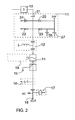
- Figure 2 shows a simplified block diagram of the disturbance protection of the output port 18 of the cable television amplifier according to Figure 1 .
- the directional coupler 13 is not shown in Figure 2 .
- the high-pass filter 12 and the diode limiter 11 are shown in more detail in Figure 1 .
- the diode limiter 11 comprises a capacitor 21 functioning as a DC separator. Resistors 22 and 23 are equal in size and are used to carry out the voltage division, by which a 12 V voltage is obtained on the RF line.
- a first diode 24 is backwardly connected to the ground from an energized RF line, and a second diode 25 is forwardly connected from the RF line to the 24 V voltage.
- the first diode 24 connected in the back direction starts to conduct with - 12 V and restricts the negative voltage to - 12 V.
- the second diode 25 connected in the forward direction starts to conduct with + 12 V and restricts the positive voltage to + 12 V.
- the 12 V backward biasing is necessary since the conduction of diodes is to be avoided using the RF utility signal. Instead of the 24 V operating voltage another available operating voltage can naturally also be used. The operating voltage may therefore also be for instance 12 V.
- the diode limiter 11 may also include one or more filtering capacitors 26 and 27.
- the first overvoltage protection component is the output gas-discharge tube 17.
- the second overvoltage protection component is the output diode limiter 11 and the third overvoltage protector component is the output suppressor 16.
- the properties of these three overvoltage protection components are very different.
- the operating voltage of the output diode limiter 11 is lower than the operating voltage of the output suppressor 16 and also the operating voltage of the output suppressor 16 is lower than the operating voltage of the output gas-discharge tube 17.
- the response time of the output suppressor 16 is faster than the response time of the output gas-discharge tube 17.
- the response time of the output diode limiter 11 is faster than the response time of the output suppressor 16.
- the input gas-discharge tube 2 is a fourth overvoltage protector component and the input diode limiter 8 is a fifth overvoltage protection component.
- the input suppressor 3 is, in turn, correspondingly a sixth overvoltage protection component.
- the input diode limiter 8 correspondingly has a lower operating voltage than the input suppressor 3 and the input suppressor 3 has a lower operating voltage than the input gas-discharge tube 2.
- the input diode limiter 8 has a faster response time than the input suppressor 3 and the input suppressor 3 has a faster response time than the input gas-discharge tube 2.
- a telecommunications device in which the disturbance protection is arranged may a cable television amplifier provided with an optical input, in which case the above disturbance protection is arranged in connection with the output port.
- the disturbance protection shown above can be applied for protecting other telecommunications devices used in a telecommunications network, such as a switch or a router or similar telecommunications devices.
Landscapes
- Engineering & Computer Science (AREA)
- Power Engineering (AREA)
- Emergency Protection Circuit Devices (AREA)
- Two-Way Televisions, Distribution Of Moving Picture Or The Like (AREA)
Description
- The invention relates to a disturbance protection system for a telecommunications device, the telecommunications device comprising an input port, an output port and a part to be protected implemented by means of semi-conductor components.
- Among telecommunications devices for instance cable television amplifier components are typically protected in such a manner that a gas-discharge tube is arranged at the input and output ports. A gas-discharge tube protects from a surge wave so that a disruptive discharge occurs in the gas-discharge tube starting from a certain voltage level that short circuits most of the energy in the surge wave to the ground. However, the gas-discharge tube is not alone able to protect the cable television amplifier components adequately enough for instance from an electrostatic discharge, in other words from what is known as an ESD pulse. Therefore, a diode limiter has also been used in a cable television amplifier for protecting the components. In order to ensure durability, the diode limiter is positioned as close as possible to the component to be protected, in which case one diode limiter does not necessarily protect several components, but several diode limiters would be required, if all components were to be protected. Problems have also been observed concerning the durability of the diode limiter, and therefore better solutions for protecting cable television amplifier components need to be developed.
-
Patent publication US4887180 discloses a device for protecting electronic equipment against strong electromagnetic pulses, comprising two series-connected dischargers followed by a filter having a cut-off frequency dependent of the output level of the second discharger. - It is an object of the present invention to provide a new type of disturbance protection for a telecommunications device that is improved in comparison with the prior art.
- The disturbance protection according to the invention is characterized in that the disturbance protection system comprises at least three overvoltage protection components provided with different properties, whereby a gas-discharge tube, which is considered as a first overvoltage protection component, is arranged at the output port, and a second overvoltage protection component is provided in the vicinity of the components to be protected, and the disturbance protection system also comprises a third overvoltage protection component.
- It is an essential idea of the invention that a gas-discharge tube, which is the first overvoltage protection component, provided at the output port and the second overvoltage protection component in the vicinity of the telecommunications device are arranged to protect the components in a telecommunications device. A third overvoltage protection component is also included in the disturbance protection system. The different overvoltage protection components are provided with different properties. Thus, an extremely good immunity is obtained for the components in the telecommunications device, for instance against surge wave pulses and ESD pulses. A gas-discharge tube offers extremely good protection against a surge wave pulse. The other overvoltage protection components then again protect for instance the amplifier circuit as regards the surge wave pulse thereof that is not filtered by the gas-discharge tube. Furthermore, the second overvoltage protector may provide adequate protection for instance against an ESD pulse and the third overvoltage protector may offer additional protection against an ESD pulse and protect in particular the second overvoltage protector from breakdown.
- The idea of an embodiment is that the telecommunications device is a cable television amplifier comprising components for processing a return path signal, whereby the cable television amplifier includes a diplexer that is arranged between the output and/or input port and the forward path components and the return path components, in which case the third overvoltage protector is arranged between the input and/or output port and the diplexer such that the third overvoltage protector is arranged to protect both the return path components and the forward path components. Consequently one overvoltage protector is able to protect the forward path components as well as the second overvoltage protector in connection therewith and the return path components. Typically the return path components endure disturbance pulses fairly well, in which case the third overvoltage protector is enough to protect the return path components from an ESD pulse. The idea of another embodiment is that components are also protected with a high-pass filter in the vicinity of the second overvoltage protector. Then, for instance an amplifier is extremely well protected. In addition, the high-pass filter also protects the second overvoltage protector.
- The invention will be explained in greater detail in the accompanying drawings, in which
-
Figure 1 shows a simplified block diagram of a cable television amplifier, and -
Figure 2 shows a simplified block diagram of disturbance protection at one RF port. -
Figure 1 shows a simplified block diagram of a cable television amplifier. InFigure 1 arrows A illustrate the course of a forward path signal and arrows B correspondingly illustrate the course of a return path signal. What is meant by a forward path signal is, for instance, a TV program signal distributed by a service producer such as a cable television company to the customer, or the consumer. A return path signal is in turn, for instance, a signal assigned by the customer, or the consumer, to the service producer. - The cable television amplifier comprises an
input port 1, after which an input gas-discharge tube 2 is arranged. An input suppressor 3 is arranged after the input gas-discharge tube 2. In this specification the term "suppressor" refers to bi-directional semiconductor ESD protection, such as product 0603 ESDA Suppressor of the Cooper-Bussman company. - A tap used to form an
input test point 4 is provided after the input suppressor 3. The suppressor 3 can also be arranged at the tap. Aninput diplexer 5 is provided after theinput test point 4. Thediplexer 5 directs the forward path signal and the return path signal to travel along the routes illustrated by arrows A and B inFigure 1 . - Next, an
input attenuator 6 and a signal inclination controller 7 are provided on the route of the forward path signal. Aninput diode limiter 8 is arranged before aninput amplifier 9. Anoutput amplifier 10 is arranged after theinput amplifier 9 and intermediate control components are in turn provided between theinput amplifier 9 and theoutput amplifier 10, meaning attenuator and inclination control components of corresponding type as those before theinput amplifier 9. - An
output diode limiter 11 is then arranged in the vicinity of theoutput amplifier 10 and a filtering component, i.e. a high-pass filter 12, is arranged in the vicinity of theoutput diode limiter 11. - A
directional coupler 13 is arranged after the high-pass filter 12 so as to be able to take a sample for measuring the level of the forward path signal. The sample is also utilized for processing the return path signal. An output diplexer is provided after thedirectional coupler 13. Theoutput diplexer 14 operates in a similar manner as theinput diplexer 5. - A tap is arranged after the
output diplexer 14 for anoutput test point 15. Thereafter anoutput suppressor 16 is provided. Theoutput suppressor 16 is similar to the input suppressor 3. - An output gas-
discharge tube 17 that is similar to the input gas-discharge tube 2 is also provided at theoutput port 18. The number ofRF ports 18 may also be greater than the only oneinput port 1 and oneoutput port 18 shown inFigure 1 . - For processing the return path signal the cable television amplifier is provided with return path components within the area surrounded by a
dashed line 19. The return path components include for instance areturn path amplifier 20, attenuators and inclination controllers and other components corresponding to those in connection with the forward path components. In this context, the return path components and the function thereof are not explained in more detail, since the components concerned and the function thereof are obvious to those skilled in the art. Furthermore, for clarity, no other components possibly associated with the cable television amplifier are presented in the block diagram. - The gas-
discharge tubes diode limiters path input amplifier 9 and theoutput amplifier 10. These diode limiters protect theamplifiers discharge tubes discharge tubes - The electrostatic discharge, in other words what is known as the ESD pulse rise time caused by the ESD, is very small, typically for instance 0.7 to 1 nanoseconds. Consequently the ESD pulse does not cause disruptive discharge in the gas-
discharge tubes suppressors 3 and 16 are bi-directional ESD disturbance attenuators. Thesuppressors 3 and 16 start conducting with voltage ± 125 V and the suppressors restrict the voltage to ± 35 V. What has been observed in tests is that a single suppressor is not adequate enough to protect theforward path amplifiers suppressors 3 and 16 protect thediode limiters suppressors 3 and 16 protect the forward path components from ESD pulses, since they are arranged between a diplexer and an RF port, i.e. for instance between theinput diplexer 5 and theinput port 1 and theoutput diplexer 14 and theoutput port 18, in other words at a location where both the forward path signal and the return path signal proceed. The return path components are more insensitive towards the ESD pulses than the forward path components, in which case thesuppressors 3 and 16 are adequate to protect them from ESD pulses. - The high-
pass filter 12 is a conventional single-stage filter. The angular frequency of the high-pass filter 12 is forinstance 20 MHz. Thus, the high-pass filter 12 attenuates the frequencies lower than five megahertz with over 35 decibels. The high-pass filter 12 is required for instance when the return path components are not used, in which case thediplexers diplexers diplexers return path amplifier pass filter 12 is required especially to protect theoutput amplifier 10. The high-pass filter is not necessarily required to protect the forward path input amplifier, since amplifier components provided with a fairly good ESD and surge wave pulse duration are typically used as theoutput amplifier 10. - The
diode limiters input amplifier 9 and theoutput amplifier 10 from an ESD pulse and a surge wave pulse. Thediode limiters diode limiters pass filter 12 is also placed as far as possible from the RF port. What is to be avoided in this way is the breakdown of the diode limiter and the high-pass filter by impact of the ESD or surge wave pulse. - In essence, the
suppressors 3 and 16 thus enable to protect the return path components from the ESD pulse. The high-pass filter 12 protects thediode limiter 11 and the amplifier circuit irrespective of whether the diplexer is in use or whether it is replaced with what is known as a zero dB plug-in unit. Thus also the amplifier circuits implemented using the new GaAs technique that is more sensitive to disturbance are extremely well protected from ESD and surge wave pulses. -
Figure 2 shows a simplified block diagram of the disturbance protection of theoutput port 18 of the cable television amplifier according toFigure 1 . For clarity, thedirectional coupler 13 is not shown inFigure 2 . The high-pass filter 12 and thediode limiter 11 are shown in more detail inFigure 1 . - The
diode limiter 11 comprises acapacitor 21 functioning as a DC separator.Resistors first diode 24 is backwardly connected to the ground from an energized RF line, and asecond diode 25 is forwardly connected from the RF line to the 24 V voltage. Thefirst diode 24 connected in the back direction starts to conduct with - 12 V and restricts the negative voltage to - 12 V. Thesecond diode 25 connected in the forward direction starts to conduct with + 12 V and restricts the positive voltage to + 12 V. The 12 V backward biasing is necessary since the conduction of diodes is to be avoided using the RF utility signal. Instead of the 24 V operating voltage another available operating voltage can naturally also be used. The operating voltage may therefore also be for instance 12 V. Thediode limiter 11 may also include one ormore filtering capacitors 26 and 27. - In the above example the first overvoltage protection component is the output gas-
discharge tube 17. The second overvoltage protection component is theoutput diode limiter 11 and the third overvoltage protector component is theoutput suppressor 16. The properties of these three overvoltage protection components are very different. The operating voltage of theoutput diode limiter 11 is lower than the operating voltage of theoutput suppressor 16 and also the operating voltage of theoutput suppressor 16 is lower than the operating voltage of the output gas-discharge tube 17. Furthermore, the response time of theoutput suppressor 16 is faster than the response time of the output gas-discharge tube 17. Also, the response time of theoutput diode limiter 11 is faster than the response time of theoutput suppressor 16. - Moreover, in
Figure 1 the input gas-discharge tube 2 is a fourth overvoltage protector component and theinput diode limiter 8 is a fifth overvoltage protection component. The input suppressor 3 is, in turn, correspondingly a sixth overvoltage protection component. Thus, theinput diode limiter 8 correspondingly has a lower operating voltage than the input suppressor 3 and the input suppressor 3 has a lower operating voltage than the input gas-discharge tube 2. In addition theinput diode limiter 8 has a faster response time than the input suppressor 3 and the input suppressor 3 has a faster response time than the input gas-discharge tube 2. - The drawings and the specification associated therewith are merely intended to illustrate the idea of the invention. The details of the invention may vary within the scope of the claims. Thus, the above disturbance protection is extremely well suitable to be used in connection with co-axial input and output ports. A telecommunications device in which the disturbance protection is arranged may a cable television amplifier provided with an optical input, in which case the above disturbance protection is arranged in connection with the output port. Furthermore the disturbance protection shown above can be applied for protecting other telecommunications devices used in a telecommunications network, such as a switch or a router or similar telecommunications devices.
Claims (8)
- A telecommunications device comprising an input port (1), an output port (18) , a part to be protected implemented by means of semi-conductor and a disturbance protection system, characterized in that the disturbance protection system comprises at least three overvoltage protection components provided with different properties, whereby a gas-discharge tube (17), which is considered as a first overvoltage protection component, is arranged at the output port (18), and a second overvoltage protection component (11) is provided in the vicinity of the components to be protected (10), and the disturbance protection system also comprises a third overvoltage protection component, that the third overvoltage protection component (16) is arranged between the first overvoltage protection component and the second overvoltage protection component and the second overvoltage protection component has a lower operating voltage than the third overvoltage protection component and the third overvoltage protection component has a lower operating voltage than the first overvoltage protection component and that the second overvoltage protection component has a faster response time than the third overvoltage protection component and the third overvoltage protection component has a faster response time than the first overvoltage protection component.
- A telecommunications device as claimed in claim 1, characterized in that the disturbance protection system also includes a high-pass filter (12) for protecting the second overvoltage protection component.
- A telecommunications device as claimed in claim 1 or 2, characterized in that the telecommunications device is a cable television amplifier.
- A telecommunications device as claimed in claim 3, characterized in that the cable television amplifier comprises components for processing forward path signals, components for processing return path signals and diplexers (5, 14) for conducting the forward path signals and the return path signals, and that the third overvoltage protection component is arranged between the input port (1) and/or the output port (18) and the diplexers (5, 14), whereby the third overvoltage protection component is arranged to protect both the return path components and the forward path components.
- A telecommunications device as claimed in any one of the preceding claims, characterized in that the second overvoltage protection component is a diode limiter (11) and the third overvoltage protection component is a suppressor (16).
- A telecommunications device as claimed in any one of the preceding claims, characterized in that a gas-discharge tube (2) is provided at the input port (1) of the telecommunications device, and said gas-discharge tube is a fourth overvoltage protection component, and that a fifth overvoltage protection component is provided in the vicinity of the components to be protected and that a sixth overvoltage protection component is provided between the fourth overvoltage protection component and the fifth overvoltage protection component.
- A telecommunications device as claimed in claim 6, char-acterized in that the operating voltage of the fifth overvoltage protection component is lower than the operating voltage of the sixth overvoltage protection component, and the operating voltage of the sixth overvoltage protection component is lower than the operating voltage of the fourth overvoltage protection component.
- A telecommunications device as claimed in claim 6 or 7, characterized in that the high-pass filter (12) is arranged to protect the second overvoltage protection component, but no high-pass filter is provided at the input port (1).
Priority Applications (1)
| Application Number | Priority Date | Filing Date | Title |
|---|---|---|---|
| PL05102325T PL1580880T3 (en) | 2004-03-24 | 2005-03-23 | Interference protection for telecommunications equipment |
Applications Claiming Priority (2)
| Application Number | Priority Date | Filing Date | Title |
|---|---|---|---|
| FI20045096 | 2004-03-24 | ||
| FI20045096A FI118108B (en) | 2004-03-24 | 2004-03-24 | Interference protection for data communication devices |
Publications (2)
| Publication Number | Publication Date |
|---|---|
| EP1580880A1 EP1580880A1 (en) | 2005-09-28 |
| EP1580880B1 true EP1580880B1 (en) | 2016-10-12 |
Family
ID=32039524
Family Applications (1)
| Application Number | Title | Priority Date | Filing Date |
|---|---|---|---|
| EP05102325.7A Expired - Lifetime EP1580880B1 (en) | 2004-03-24 | 2005-03-23 | Disturbance protection for a telecommunications device |
Country Status (4)
| Country | Link |
|---|---|
| EP (1) | EP1580880B1 (en) |
| ES (1) | ES2610464T3 (en) |
| FI (1) | FI118108B (en) |
| PL (1) | PL1580880T3 (en) |
Family Cites Families (3)
| Publication number | Priority date | Publication date | Assignee | Title |
|---|---|---|---|---|
| FR2576471B1 (en) * | 1985-01-24 | 1988-03-18 | Cables De Lyon Geoffroy Delore | DEVICE FOR PROTECTING A HIGH FREQUENCY COAXIAL LINE AGAINST INTERFERENCE PULSES |
| DE3864328D1 (en) * | 1987-06-16 | 1991-09-26 | Commissariat Energie Atomique | PROTECTIVE DEVICE FOR AN ELECTRONIC DEVICE AGAINST STRONG ELECTROMAGNETIC IMPULSES, ESPECIALLY CALLED BY LIGHTNING. |
| US5390337A (en) * | 1992-05-01 | 1995-02-14 | Scientific-Atlanta, Inc. | Combination surge and diplex filter for CATV distribution systems |
-
2004
- 2004-03-24 FI FI20045096A patent/FI118108B/en active IP Right Grant
-
2005
- 2005-03-23 PL PL05102325T patent/PL1580880T3/en unknown
- 2005-03-23 EP EP05102325.7A patent/EP1580880B1/en not_active Expired - Lifetime
- 2005-03-23 ES ES05102325.7T patent/ES2610464T3/en not_active Expired - Lifetime
Also Published As
| Publication number | Publication date |
|---|---|
| FI20045096A0 (en) | 2004-03-24 |
| FI20045096L (en) | 2005-09-25 |
| PL1580880T3 (en) | 2017-06-30 |
| EP1580880A1 (en) | 2005-09-28 |
| ES2610464T3 (en) | 2017-04-27 |
| FI118108B (en) | 2007-06-29 |
Similar Documents
| Publication | Publication Date | Title |
|---|---|---|
| US5966283A (en) | Surge suppression for radio frequency transmission lines | |
| US5625521A (en) | Surge protection circuitry | |
| US6195245B1 (en) | Low capacitance surge protector for high speed data transmission | |
| US7082022B2 (en) | Circuit for diverting surges and transient impulses | |
| US7221550B2 (en) | Surge protection device and method | |
| KR101171228B1 (en) | Protection devices for power line against high altitude electromagnetic pulse | |
| US7457093B2 (en) | Protection and indication apparatus | |
| US20130208380A1 (en) | Transient control technology circuit | |
| EP1580880A1 (en) | Disturbance protection for a telecommunications device | |
| EP1018201B1 (en) | Solid-state high voltage crowbar circuit | |
| KR101473740B1 (en) | Apparatus for high frequency signal reduction | |
| JPH1094168A (en) | Lightning protection circuit | |
| JP2000050494A (en) | Arrester for coaxial cable | |
| KR101454294B1 (en) | Signal-selective protection device | |
| US20250210979A1 (en) | Electrical overstress protection device and communication system | |
| KR200317413Y1 (en) | A serge protecting apparatus for image processing devices | |
| GB2176956A (en) | Voltage and current transient protection | |
| TW202529354A (en) | Electrical overstress protection device and communication system | |
| KR101556551B1 (en) | Surge protecting apparatus for protecting follow current in dc line | |
| EP0827316A2 (en) | A device for protecting a telecommunications apparatus | |
| CN1409536A (en) | Mobile communication equipment with static discharging protection | |
| CN116207728A (en) | General electromagnetic pulse protection method for multiple interfaces and application | |
| KR19990021001A (en) | Surge voltage protection device of communication terminal | |
| CN111009890A (en) | Multi-channel network port electromagnetic pulse protection module for Ethernet |
Legal Events
| Date | Code | Title | Description |
|---|---|---|---|
| PUAI | Public reference made under article 153(3) epc to a published international application that has entered the european phase |
Free format text: ORIGINAL CODE: 0009012 |
|
| AK | Designated contracting states |
Kind code of ref document: A1 Designated state(s): AT BE BG CH CY CZ DE DK EE ES FI FR GB GR HU IE IS IT LI LT LU MC NL PL PT RO SE SI SK TR |
|
| AX | Request for extension of the european patent |
Extension state: AL BA HR LV MK YU |
|
| 17P | Request for examination filed |
Effective date: 20060320 |
|
| AKX | Designation fees paid |
Designated state(s): AT BE BG CH CY CZ DE DK EE ES FI FR GB GR HU IE IS IT LI LT LU MC NL PL PT RO SE SI SK TR |
|
| 17Q | First examination report despatched |
Effective date: 20061127 |
|
| GRAP | Despatch of communication of intention to grant a patent |
Free format text: ORIGINAL CODE: EPIDOSNIGR1 |
|
| INTG | Intention to grant announced |
Effective date: 20160323 |
|
| GRAS | Grant fee paid |
Free format text: ORIGINAL CODE: EPIDOSNIGR3 |
|
| RAP1 | Party data changed (applicant data changed or rights of an application transferred) |
Owner name: TELESTE OYJ |
|
| GRAA | (expected) grant |
Free format text: ORIGINAL CODE: 0009210 |
|
| AK | Designated contracting states |
Kind code of ref document: B1 Designated state(s): AT BE BG CH CY CZ DE DK EE ES FI FR GB GR HU IE IS IT LI LT LU MC NL PL PT RO SE SI SK TR |
|
| REG | Reference to a national code |
Ref country code: GB Ref legal event code: FG4D |
|
| REG | Reference to a national code |
Ref country code: CH Ref legal event code: EP |
|
| REG | Reference to a national code |
Ref country code: AT Ref legal event code: REF Ref document number: 837301 Country of ref document: AT Kind code of ref document: T Effective date: 20161015 |
|
| REG | Reference to a national code |
Ref country code: IE Ref legal event code: FG4D |
|
| REG | Reference to a national code |
Ref country code: DE Ref legal event code: R096 Ref document number: 602005050403 Country of ref document: DE |
|
| REG | Reference to a national code |
Ref country code: NL Ref legal event code: FP |
|
| REG | Reference to a national code |
Ref country code: LT Ref legal event code: MG4D |
|
| REG | Reference to a national code |
Ref country code: ES Ref legal event code: FG2A Ref document number: 2610464 Country of ref document: ES Kind code of ref document: T3 Effective date: 20170427 |
|
| PG25 | Lapsed in a contracting state [announced via postgrant information from national office to epo] |
Ref country code: LT Free format text: LAPSE BECAUSE OF FAILURE TO SUBMIT A TRANSLATION OF THE DESCRIPTION OR TO PAY THE FEE WITHIN THE PRESCRIBED TIME-LIMIT Effective date: 20161012 Ref country code: SE Free format text: LAPSE BECAUSE OF FAILURE TO SUBMIT A TRANSLATION OF THE DESCRIPTION OR TO PAY THE FEE WITHIN THE PRESCRIBED TIME-LIMIT Effective date: 20161012 Ref country code: GR Free format text: LAPSE BECAUSE OF FAILURE TO SUBMIT A TRANSLATION OF THE DESCRIPTION OR TO PAY THE FEE WITHIN THE PRESCRIBED TIME-LIMIT Effective date: 20170113 |
|
| PG25 | Lapsed in a contracting state [announced via postgrant information from national office to epo] |
Ref country code: BE Free format text: LAPSE BECAUSE OF FAILURE TO SUBMIT A TRANSLATION OF THE DESCRIPTION OR TO PAY THE FEE WITHIN THE PRESCRIBED TIME-LIMIT Effective date: 20161012 Ref country code: IS Free format text: LAPSE BECAUSE OF FAILURE TO SUBMIT A TRANSLATION OF THE DESCRIPTION OR TO PAY THE FEE WITHIN THE PRESCRIBED TIME-LIMIT Effective date: 20170212 Ref country code: FI Free format text: LAPSE BECAUSE OF FAILURE TO SUBMIT A TRANSLATION OF THE DESCRIPTION OR TO PAY THE FEE WITHIN THE PRESCRIBED TIME-LIMIT Effective date: 20161012 Ref country code: PT Free format text: LAPSE BECAUSE OF FAILURE TO SUBMIT A TRANSLATION OF THE DESCRIPTION OR TO PAY THE FEE WITHIN THE PRESCRIBED TIME-LIMIT Effective date: 20170213 |
|
| REG | Reference to a national code |
Ref country code: DE Ref legal event code: R097 Ref document number: 602005050403 Country of ref document: DE |
|
| PG25 | Lapsed in a contracting state [announced via postgrant information from national office to epo] |
Ref country code: SK Free format text: LAPSE BECAUSE OF FAILURE TO SUBMIT A TRANSLATION OF THE DESCRIPTION OR TO PAY THE FEE WITHIN THE PRESCRIBED TIME-LIMIT Effective date: 20161012 Ref country code: CZ Free format text: LAPSE BECAUSE OF FAILURE TO SUBMIT A TRANSLATION OF THE DESCRIPTION OR TO PAY THE FEE WITHIN THE PRESCRIBED TIME-LIMIT Effective date: 20161012 Ref country code: EE Free format text: LAPSE BECAUSE OF FAILURE TO SUBMIT A TRANSLATION OF THE DESCRIPTION OR TO PAY THE FEE WITHIN THE PRESCRIBED TIME-LIMIT Effective date: 20161012 Ref country code: DK Free format text: LAPSE BECAUSE OF FAILURE TO SUBMIT A TRANSLATION OF THE DESCRIPTION OR TO PAY THE FEE WITHIN THE PRESCRIBED TIME-LIMIT Effective date: 20161012 Ref country code: RO Free format text: LAPSE BECAUSE OF FAILURE TO SUBMIT A TRANSLATION OF THE DESCRIPTION OR TO PAY THE FEE WITHIN THE PRESCRIBED TIME-LIMIT Effective date: 20161012 |
|
| PLBE | No opposition filed within time limit |
Free format text: ORIGINAL CODE: 0009261 |
|
| STAA | Information on the status of an ep patent application or granted ep patent |
Free format text: STATUS: NO OPPOSITION FILED WITHIN TIME LIMIT |
|
| PG25 | Lapsed in a contracting state [announced via postgrant information from national office to epo] |
Ref country code: BG Free format text: LAPSE BECAUSE OF FAILURE TO SUBMIT A TRANSLATION OF THE DESCRIPTION OR TO PAY THE FEE WITHIN THE PRESCRIBED TIME-LIMIT Effective date: 20170112 Ref country code: IT Free format text: LAPSE BECAUSE OF FAILURE TO SUBMIT A TRANSLATION OF THE DESCRIPTION OR TO PAY THE FEE WITHIN THE PRESCRIBED TIME-LIMIT Effective date: 20161012 |
|
| 26N | No opposition filed |
Effective date: 20170713 |
|
| REG | Reference to a national code |
Ref country code: DE Ref legal event code: R119 Ref document number: 602005050403 Country of ref document: DE |
|
| REG | Reference to a national code |
Ref country code: CH Ref legal event code: PL |
|
| PG25 | Lapsed in a contracting state [announced via postgrant information from national office to epo] |
Ref country code: SI Free format text: LAPSE BECAUSE OF FAILURE TO SUBMIT A TRANSLATION OF THE DESCRIPTION OR TO PAY THE FEE WITHIN THE PRESCRIBED TIME-LIMIT Effective date: 20161012 Ref country code: MC Free format text: LAPSE BECAUSE OF FAILURE TO SUBMIT A TRANSLATION OF THE DESCRIPTION OR TO PAY THE FEE WITHIN THE PRESCRIBED TIME-LIMIT Effective date: 20161012 |
|
| REG | Reference to a national code |
Ref country code: FR Ref legal event code: ST Effective date: 20171130 |
|
| PG25 | Lapsed in a contracting state [announced via postgrant information from national office to epo] |
Ref country code: FR Free format text: LAPSE BECAUSE OF NON-PAYMENT OF DUE FEES Effective date: 20170331 Ref country code: DE Free format text: LAPSE BECAUSE OF NON-PAYMENT OF DUE FEES Effective date: 20171003 Ref country code: LU Free format text: LAPSE BECAUSE OF NON-PAYMENT OF DUE FEES Effective date: 20170323 |
|
| PG25 | Lapsed in a contracting state [announced via postgrant information from national office to epo] |
Ref country code: LI Free format text: LAPSE BECAUSE OF NON-PAYMENT OF DUE FEES Effective date: 20170331 Ref country code: CH Free format text: LAPSE BECAUSE OF NON-PAYMENT OF DUE FEES Effective date: 20170331 |
|
| PG25 | Lapsed in a contracting state [announced via postgrant information from national office to epo] |
Ref country code: HU Free format text: LAPSE BECAUSE OF FAILURE TO SUBMIT A TRANSLATION OF THE DESCRIPTION OR TO PAY THE FEE WITHIN THE PRESCRIBED TIME-LIMIT; INVALID AB INITIO Effective date: 20050323 |
|
| REG | Reference to a national code |
Ref country code: AT Ref legal event code: UEP Ref document number: 837301 Country of ref document: AT Kind code of ref document: T Effective date: 20161012 |
|
| PG25 | Lapsed in a contracting state [announced via postgrant information from national office to epo] |
Ref country code: CY Free format text: LAPSE BECAUSE OF NON-PAYMENT OF DUE FEES Effective date: 20161012 |
|
| PG25 | Lapsed in a contracting state [announced via postgrant information from national office to epo] |
Ref country code: TR Free format text: LAPSE BECAUSE OF FAILURE TO SUBMIT A TRANSLATION OF THE DESCRIPTION OR TO PAY THE FEE WITHIN THE PRESCRIBED TIME-LIMIT Effective date: 20161012 |
|
| PGFP | Annual fee paid to national office [announced via postgrant information from national office to epo] |
Ref country code: IE Payment date: 20220323 Year of fee payment: 18 Ref country code: GB Payment date: 20220321 Year of fee payment: 18 Ref country code: AT Payment date: 20220322 Year of fee payment: 18 |
|
| PGFP | Annual fee paid to national office [announced via postgrant information from national office to epo] |
Ref country code: PL Payment date: 20220310 Year of fee payment: 18 Ref country code: NL Payment date: 20220321 Year of fee payment: 18 |
|
| PGFP | Annual fee paid to national office [announced via postgrant information from national office to epo] |
Ref country code: ES Payment date: 20220525 Year of fee payment: 18 |
|
| REG | Reference to a national code |
Ref country code: NL Ref legal event code: MM Effective date: 20230401 |
|
| REG | Reference to a national code |
Ref country code: AT Ref legal event code: MM01 Ref document number: 837301 Country of ref document: AT Kind code of ref document: T Effective date: 20230323 |
|
| GBPC | Gb: european patent ceased through non-payment of renewal fee |
Effective date: 20230323 |
|
| PG25 | Lapsed in a contracting state [announced via postgrant information from national office to epo] |
Ref country code: NL Free format text: LAPSE BECAUSE OF NON-PAYMENT OF DUE FEES Effective date: 20230401 |
|
| REG | Reference to a national code |
Ref country code: IE Ref legal event code: MM4A |
|
| PG25 | Lapsed in a contracting state [announced via postgrant information from national office to epo] |
Ref country code: GB Free format text: LAPSE BECAUSE OF NON-PAYMENT OF DUE FEES Effective date: 20230323 |
|
| PG25 | Lapsed in a contracting state [announced via postgrant information from national office to epo] |
Ref country code: IE Free format text: LAPSE BECAUSE OF NON-PAYMENT OF DUE FEES Effective date: 20230323 Ref country code: GB Free format text: LAPSE BECAUSE OF NON-PAYMENT OF DUE FEES Effective date: 20230323 Ref country code: AT Free format text: LAPSE BECAUSE OF NON-PAYMENT OF DUE FEES Effective date: 20230323 |
|
| REG | Reference to a national code |
Ref country code: ES Ref legal event code: FD2A Effective date: 20240506 |
|
| PG25 | Lapsed in a contracting state [announced via postgrant information from national office to epo] |
Ref country code: ES Free format text: LAPSE BECAUSE OF NON-PAYMENT OF DUE FEES Effective date: 20230324 |
|
| PG25 | Lapsed in a contracting state [announced via postgrant information from national office to epo] |
Ref country code: ES Free format text: LAPSE BECAUSE OF NON-PAYMENT OF DUE FEES Effective date: 20230324 |
|
| PG25 | Lapsed in a contracting state [announced via postgrant information from national office to epo] |
Ref country code: PL Free format text: LAPSE BECAUSE OF NON-PAYMENT OF DUE FEES Effective date: 20230323 |
|
| PG25 | Lapsed in a contracting state [announced via postgrant information from national office to epo] |
Ref country code: PL Free format text: LAPSE BECAUSE OF NON-PAYMENT OF DUE FEES Effective date: 20230323 |