EP1580659A1 - A method and system for configuration of processor integrated devices in multi-processor systems - Google Patents
A method and system for configuration of processor integrated devices in multi-processor systems Download PDFInfo
- Publication number
- EP1580659A1 EP1580659A1 EP04257322A EP04257322A EP1580659A1 EP 1580659 A1 EP1580659 A1 EP 1580659A1 EP 04257322 A EP04257322 A EP 04257322A EP 04257322 A EP04257322 A EP 04257322A EP 1580659 A1 EP1580659 A1 EP 1580659A1
- Authority
- EP
- European Patent Office
- Prior art keywords
- processor
- configuration
- chipset
- pci
- integrated device
- Prior art date
- Legal status (The legal status is an assumption and is not a legal conclusion. Google has not performed a legal analysis and makes no representation as to the accuracy of the status listed.)
- Granted
Links
Images



Classifications
-
- G—PHYSICS
- G06—COMPUTING OR CALCULATING; COUNTING
- G06F—ELECTRIC DIGITAL DATA PROCESSING
- G06F15/00—Digital computers in general; Data processing equipment in general
- G06F15/16—Combinations of two or more digital computers each having at least an arithmetic unit, a program unit and a register, e.g. for a simultaneous processing of several programs
-
- G—PHYSICS
- G06—COMPUTING OR CALCULATING; COUNTING
- G06F—ELECTRIC DIGITAL DATA PROCESSING
- G06F13/00—Interconnection of, or transfer of information or other signals between, memories, input/output devices or central processing units
- G06F13/38—Information transfer, e.g. on bus
- G06F13/40—Bus structure
- G06F13/4004—Coupling between buses
- G06F13/4027—Coupling between buses using bus bridges
Definitions
- This disclosure generally relates to configuration, specifically, relating to configuration of integrated devices incorporated within processors or network components in multi-processor systems.
- processors are incorporated along with other integrated devices, such as, memory controllers or coprocessors into a single integrated device package.
- the corresponding processor package is configurable by operating system (OS) plug-and-play configuration software.
- OS operating system
- the configuration software utilizes established configuration mechanism as defined by Peripheral Component Interconnect (PCI) or PCI Express specifications.
- PCI Peripheral Component Interconnect
- PCI Express Peripheral Component Interconnect
- the configuration mechanisms utilize memory or Input/Output (IO) mapped configuration region for generating configuration transactions on the respective interconnect.
- One example of configuration is done by a chipset, as depicted in connection with Figure 1.
- a chipset In order to configure Integrated Device 1 (incorporated within Processor 2), a chipset translates the required configuration cycle. Therefore, the chipset needs to route the configuration cycle from either processor 1 or processor 2 back to processor 2.
- current generation processor buses do not have supported configuration cycles for this routing.
- Another configuration example is the processor internally decoding the memory or IO access for configuration and not generating an access to the chipset for the integrated device 1. However, this does not allow for configuration accesses from processor 1 to be routed to the integrated device 1 in processor 2 due to lack of configuration cycles on current processor buses.
- shrink wrap operating systems may be used for configuration. However, they do not support situations where an integrated device is visible from some processors but not others.
- An area of current technological development relates to being able to configure integrated devices within a processor or network component. As previously described, chipsets translate the configuration cycle. Also, prior art configuration schemes are not supported by processor buses for multiprocessor systems.
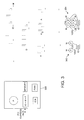
- the claimed subject matter supports configuration by facilitating translation of the memory or IO mapped configuration access from a processor to a PCI or PCI Express configuration cycle and is done natively by the processor, as depicted in connection with Figure 2.
- FIG. 2 is an apparatus to facilitate configuration of an integrated device by a processor in accordance with the claimed subject matter.
- the apparatus depicts a decoder in processor 1.
- the decoder is discussed further in connection with Figure 4.
- the decoder internally converts a memory or IO access for configuration to a configuration cycle.
- the prior art facilitates the chipset translating the configuration cycle.
- the configuration cycle is routed either to a chipset or to the integrated device in processor 2 based at least in part on routing information.
- the chipset receives the configuration access from the decoder via a network fabric. Subsequently, the chipset forwards the translated configuration access via a PCI or PCI Express Interconnect.
- the integrated device receives the configuration access via a network fabric.
- the routing of the configuration cycle to either the chipset or integrated device is based at least in part on the routing information.
- the network fabric is discussed in further detail in connection with Figure 3.
- an integrated device may be configured while using the existing configuration mechanisms for the PCI or PCI Express interconnects.
- the claimed subject matter does not suffer from processor affinity issues since the entire configuration space is globally visible to all components (i.e. all devices are visible to all processors). Therefore, the claimed subject matter enables processor and/or network components with integrated devices in multi-processor systems to be configured by existing shrink-wrap operating systems.
- the method for configuration depicted in Figure 2 is incorporated and implemented in software.
- the software may be stored in an electronically-accessible medium that includes any mechanism that provides (i.e., stores and/or transmits) content (e.g., computer executable instructions) in a form readable by an electronic device (e.g., a computer, a personal digital assistant, a cellular telephone).
- a machine-accessible medium includes read only memory (ROM); random access memory (RAM); magnetic disk storage media; optical storage media; flash memory devices; electrical, optical, acoustical or other form of propagated signals (e.g., carrier waves, infrared signals, digital signals).
- Figure 3 depicts a point to point system with one or more processors.
- the claimed subject matter comprises several embodiments, one with one processor 306, one with two processors (P) 302 and one with four processors (P) 304.
- each processor is coupled to a memory (M) and is connected to each processor via a network fabric may comprise either or all of: a link layer, a protocol layer, a routing layer, a transport layer, and a physical layer.
- the fabric facilitates transporting messages from one protocol (home or caching agent) to another protocol for a point to point network.
- the system of a network fabric supports any of the embodiments depicted in connection with embodiments depicted in Figures 2 and 4..
- the uni-processor P is coupled to graphics and memory control, depicted as IO+M+F, via a network fabric link that corresponds to a layered protocol scheme.
- the graphics and memory control is coupled to memory and is capable of receiving and transmitting via PCI Express Links.
- the graphics and memory control is coupled to the ICH.
- the ICH is coupled to a firmware hub (FWH) via a LPC bus.
- FWH firmware hub
- the processor would have external network fabric links.
- the processor may have multiple cores with split or shared caches with each core coupled to a Xbar router and a non-routing global links interface.
- the external network fabric links are coupled to the Xbar router and a non-routing global links interface.
- Figure 4 is a decoder as utilized by one embodiment.
- the decoder receives a configuration address (config address).
- the config address may come from either a memory address (e.g. IPF and PCI-E Enhanced Config) or from a register internal to the CPU.. If the config address is from a memory address, the Addr decoder indicates that it's a Config cycle. Otherwise, this is determined prior to the Addr decoder Based on the config address, a nodeID and a port number is retrieved and forwarded as part of the configuration request.
Landscapes
- Engineering & Computer Science (AREA)
- Theoretical Computer Science (AREA)
- General Engineering & Computer Science (AREA)
- Computer Hardware Design (AREA)
- Physics & Mathematics (AREA)
- General Physics & Mathematics (AREA)
- Software Systems (AREA)
- Multi Processors (AREA)
- Hardware Redundancy (AREA)
- Data Exchanges In Wide-Area Networks (AREA)
- Exchange Systems With Centralized Control (AREA)
Abstract
Description
- This disclosure generally relates to configuration, specifically, relating to configuration of integrated devices incorporated within processors or network components in multi-processor systems.
- Presently, processors are incorporated along with other integrated devices, such as, memory controllers or coprocessors into a single integrated device package. The corresponding processor package is configurable by operating system (OS) plug-and-play configuration software. For example, the configuration software utilizes established configuration mechanism as defined by Peripheral Component Interconnect (PCI) or PCI Express specifications. Typically, the configuration mechanisms utilize memory or Input/Output (IO) mapped configuration region for generating configuration transactions on the respective interconnect.
- One example of configuration is done by a chipset, as depicted in connection with Figure 1. In order to configure Integrated Device 1 (incorporated within Processor 2), a chipset translates the required configuration cycle. Therefore, the chipset needs to route the configuration cycle from either
processor 1 orprocessor 2 back toprocessor 2. However, current generation processor buses do not have supported configuration cycles for this routing. Another configuration example is the processor internally decoding the memory or IO access for configuration and not generating an access to the chipset for the integrateddevice 1. However, this does not allow for configuration accesses fromprocessor 1 to be routed to the integrateddevice 1 inprocessor 2 due to lack of configuration cycles on current processor buses. In yet another example, shrink wrap operating systems may be used for configuration. However, they do not support situations where an integrated device is visible from some processors but not others. - Subject matter is particularly pointed out and distinctly claimed in the concluding portion of the specification. The claimed subject matter, however, both as to organization and method of operation, together with objects, features, and advantages thereof, may best be understood by reference to the following detailed description when read with the accompanying drawings in which:
- FIG. 1 is a prior art method of a flowchart for configuration of an integrated device by a chipset.
- FIG. 2 is an apparatus to facilitate configuration of an integrated device by a processor in accordance with the claimed subject matter.
- FIG. 3 is a system diagram illustrating a system that may employ the embodiment of FIG. 2 or Figure 4 or both.
- FIG. 4 is a decoder as utilized by one embodiment.
-
- In the following detailed description, numerous specific details are set forth in order to provide a thorough understanding of the claimed subject matter. However, it will be understood by those skilled in the art that the claimed subject matter may be practiced without these specific details. In other instances, well-known methods, procedures, components and circuits have not been described in detail so as not to obscure the claimed subject matter.
- An area of current technological development relates to being able to configure integrated devices within a processor or network component. As previously described, chipsets translate the configuration cycle. Also, prior art configuration schemes are not supported by processor buses for multiprocessor systems.
- In contrast, the claimed subject matter supports configuration by facilitating translation of the memory or IO mapped configuration access from a processor to a PCI or PCI Express configuration cycle and is done natively by the processor, as depicted in connection with Figure 2.
- FIG. 2 is an apparatus to facilitate configuration of an integrated device by a processor in accordance with the claimed subject matter. The apparatus depicts a decoder in
processor 1. The decoder is discussed further in connection with Figure 4. In one embodiment, the decoder internally converts a memory or IO access for configuration to a configuration cycle. In contrast, the prior art facilitates the chipset translating the configuration cycle. Subsequently, the configuration cycle is routed either to a chipset or to the integrated device inprocessor 2 based at least in part on routing information. In the embodiment for routing the configuration cycle to the chipset, the chipset receives the configuration access from the decoder via a network fabric. Subsequently, the chipset forwards the translated configuration access via a PCI or PCI Express Interconnect. In the other embodiment for routing the configuration cycle to the integrated device, the integrated device receives the configuration access via a network fabric. In both of the previous embodiments, the routing of the configuration cycle to either the chipset or integrated device is based at least in part on the routing information. The network fabric is discussed in further detail in connection with Figure 3. - Therefore, an integrated device may be configured while using the existing configuration mechanisms for the PCI or PCI Express interconnects. Furthermore, the claimed subject matter does not suffer from processor affinity issues since the entire configuration space is globally visible to all components (i.e. all devices are visible to all processors). Therefore, the claimed subject matter enables processor and/or network components with integrated devices in multi-processor systems to be configured by existing shrink-wrap operating systems.
- In another embodiment for use for a PCI-Express example, there is a bridge from the chipset to
Processor 2. Upon receiving the configuration access, the chipset forwards the configuration access toprocessor 2. - In one embodiment, the method for configuration depicted in Figure 2 is incorporated and implemented in software. For example, the software may be stored in an electronically-accessible medium that includes any mechanism that provides (i.e., stores and/or transmits) content (e.g., computer executable instructions) in a form readable by an electronic device (e.g., a computer, a personal digital assistant, a cellular telephone).For example, a machine-accessible medium includes read only memory (ROM); random access memory (RAM); magnetic disk storage media; optical storage media; flash memory devices; electrical, optical, acoustical or other form of propagated signals (e.g., carrier waves, infrared signals, digital signals).
- Figure 3 depicts a point to point system with one or more processors. The claimed subject matter comprises several embodiments, one with one
processor 306, one with two processors (P) 302 and one with four processors (P) 304. Inembodiments 302 and 304, each processor is coupled to a memory (M) and is connected to each processor via a network fabric may comprise either or all of: a link layer, a protocol layer, a routing layer, a transport layer, and a physical layer. The fabric facilitates transporting messages from one protocol (home or caching agent) to another protocol for a point to point network. As previously described, the system of a network fabric supports any of the embodiments depicted in connection with embodiments depicted in Figures 2 and 4.. - For
embodiment 306, the uni-processor P is coupled to graphics and memory control, depicted as IO+M+F, via a network fabric link that corresponds to a layered protocol scheme. The graphics and memory control is coupled to memory and is capable of receiving and transmitting via PCI Express Links. Likewise, the graphics and memory control is coupled to the ICH. Furthermore, the ICH is coupled to a firmware hub (FWH) via a LPC bus. Also, for a different uni-processor embodiment, the processor would have external network fabric links. The processor may have multiple cores with split or shared caches with each core coupled to a Xbar router and a non-routing global links interface. Thus, the external network fabric links are coupled to the Xbar router and a non-routing global links interface. - Figure 4 is a decoder as utilized by one embodiment. In one embodiment, the decoder receives a configuration address (config address). In this embodiment, the config address may come from either a memory address (e.g. IPF and PCI-E Enhanced Config) or from a register internal to the CPU.. If the config address is from a memory address, the Addr decoder indicates that it's a Config cycle. Otherwise, this is determined prior to the Addr decoder Based on the config address, a nodeID and a port number is retrieved and forwarded as part of the configuration request.
- Although the claimed subject matter has been described with reference to specific embodiments, this description is not meant to be construed in a limiting sense. Various modifications of the disclosed embodiment, as well as alternative embodiments of the claimed subj ect matter, will become apparent to persons skilled in the art upon reference to the description of the claimed subject matter. It is contemplated, therefore, that such modifications can be made without departing from the spirit or scope of the claimed subject matter as defined in the appended claims.
Claims (13)
- A method for configuring an integrated device in a first processor comprising:forwarding the configuration cycle.decoding a memory configuration access within a second processor, the second processor coupled to the first processor, to a configuration cycle;routing the configuration cycle to a chipset based at least in part on a routing information; and
- The method of claim 1 wherein the configuration cycle is routed to the chipset via a network fabric.
- The method of claim 1 wherein the network fabric is a plurality of point to point links.
- The method of claim 1 wherein the chipset has a bridge and adheres to a PCI type interconnect that is either PCI or PCI Express.
- The method of claim 2 wherein the second processor is coupled to the first processor via the network fabric.
- A computer program comprising computer code means adapted to perform all the steps of any of claims 1-5 when the program is run on a computer.
- A computer program when embodied on a computer readable medium.
- A processor comprising:a decoder to decode either a memory or IO configuration access to a configuration cycle; andto transmit the configuration cycle to either a chipset or integrated device.
- The processor of claim 8 wherein the transmission of configuration cycle to either a chipset or integrated device is via a PCI type interconnect that is either PCI or PCI Express.
- The processor of claim 9 wherein the configuration cycle is routed to the integrated device or chipset via a network fabric.
- A system comprising:a first processor with an decoder coupled to a second network component with an integrated device,the decoder to decode either a memory or IO configuration access to a configuration cycle; andto transmit the configuration cycle to either a chipset or integrated device, wherein the configuration cycle adheres to a PCI type interconnect.
- The system of claim 11 wherein the PCI type interconnect is either PCI or PCI Express.
- The system of claim 11 wherein the configuration cycle is routed to the integrated device or chipset via a network fabric.
Priority Applications (1)
| Application Number | Priority Date | Filing Date | Title |
|---|---|---|---|
| EP09003501A EP2075695A3 (en) | 2004-03-22 | 2004-11-25 | Method and system for configuration of processor integrated devices in multi-processor systems |
Applications Claiming Priority (2)
| Application Number | Priority Date | Filing Date | Title |
|---|---|---|---|
| US10/806,787 US20050210229A1 (en) | 2004-03-22 | 2004-03-22 | Method and system for configuration of processor integrated devices in multi-processor systems |
| US806787 | 2004-03-22 |
Related Child Applications (1)
| Application Number | Title | Priority Date | Filing Date |
|---|---|---|---|
| EP09003501A Division EP2075695A3 (en) | 2004-03-22 | 2004-11-25 | Method and system for configuration of processor integrated devices in multi-processor systems |
Publications (2)
| Publication Number | Publication Date |
|---|---|
| EP1580659A1 true EP1580659A1 (en) | 2005-09-28 |
| EP1580659B1 EP1580659B1 (en) | 2009-04-15 |
Family
ID=34862038
Family Applications (2)
| Application Number | Title | Priority Date | Filing Date |
|---|---|---|---|
| EP09003501A Ceased EP2075695A3 (en) | 2004-03-22 | 2004-11-25 | Method and system for configuration of processor integrated devices in multi-processor systems |
| EP04257322A Expired - Lifetime EP1580659B1 (en) | 2004-03-22 | 2004-11-25 | A method and system for configuration of processor integrated devices in multi-processor systems |
Family Applications Before (1)
| Application Number | Title | Priority Date | Filing Date |
|---|---|---|---|
| EP09003501A Ceased EP2075695A3 (en) | 2004-03-22 | 2004-11-25 | Method and system for configuration of processor integrated devices in multi-processor systems |
Country Status (7)
| Country | Link |
|---|---|
| US (1) | US20050210229A1 (en) |
| EP (2) | EP2075695A3 (en) |
| KR (1) | KR100706145B1 (en) |
| CN (1) | CN100476793C (en) |
| AT (1) | ATE428970T1 (en) |
| DE (1) | DE602004020579D1 (en) |
| TW (1) | TWI311251B (en) |
Families Citing this family (13)
| Publication number | Priority date | Publication date | Assignee | Title |
|---|---|---|---|---|
| US9088474B2 (en) | 2002-10-08 | 2015-07-21 | Broadcom Corporation | Advanced processor with interfacing messaging network to a CPU |
| US7984268B2 (en) | 2002-10-08 | 2011-07-19 | Netlogic Microsystems, Inc. | Advanced processor scheduling in a multithreaded system |
| US8015567B2 (en) | 2002-10-08 | 2011-09-06 | Netlogic Microsystems, Inc. | Advanced processor with mechanism for packet distribution at high line rate |
| US7961723B2 (en) | 2002-10-08 | 2011-06-14 | Netlogic Microsystems, Inc. | Advanced processor with mechanism for enforcing ordering between information sent on two independent networks |
| US7334086B2 (en) | 2002-10-08 | 2008-02-19 | Rmi Corporation | Advanced processor with system on a chip interconnect technology |
| US7924828B2 (en) | 2002-10-08 | 2011-04-12 | Netlogic Microsystems, Inc. | Advanced processor with mechanism for fast packet queuing operations |
| US7346757B2 (en) * | 2002-10-08 | 2008-03-18 | Rmi Corporation | Advanced processor translation lookaside buffer management in a multithreaded system |
| US8176298B2 (en) | 2002-10-08 | 2012-05-08 | Netlogic Microsystems, Inc. | Multi-core multi-threaded processing systems with instruction reordering in an in-order pipeline |
| US7627721B2 (en) | 2002-10-08 | 2009-12-01 | Rmi Corporation | Advanced processor with cache coherency |
| US8037224B2 (en) | 2002-10-08 | 2011-10-11 | Netlogic Microsystems, Inc. | Delegating network processor operations to star topology serial bus interfaces |
| US8478811B2 (en) | 2002-10-08 | 2013-07-02 | Netlogic Microsystems, Inc. | Advanced processor with credit based scheme for optimal packet flow in a multi-processor system on a chip |
| US20060236016A1 (en) * | 2005-04-19 | 2006-10-19 | Tetrick R S | Method, system, and apparatus to support device configuration |
| US9596324B2 (en) | 2008-02-08 | 2017-03-14 | Broadcom Corporation | System and method for parsing and allocating a plurality of packets to processor core threads |
Citations (2)
| Publication number | Priority date | Publication date | Assignee | Title |
|---|---|---|---|---|
| EP0817089A2 (en) * | 1996-07-03 | 1998-01-07 | Intel Corporation | Processor subsystem for use with a universal computer architecture |
| US20020056037A1 (en) * | 2000-08-31 | 2002-05-09 | Gilbert Wolrich | Method and apparatus for providing large register address space while maximizing cycletime performance for a multi-threaded register file set |
Family Cites Families (2)
| Publication number | Priority date | Publication date | Assignee | Title |
|---|---|---|---|---|
| US6910108B2 (en) * | 2002-01-09 | 2005-06-21 | International Business Machines Corporation | Hardware support for partitioning a multiprocessor system to allow distinct operating systems |
| KR20040024816A (en) * | 2002-09-16 | 2004-03-22 | 위니아만도 주식회사 | Method for displaying error of kimchi storage |
-
2004
- 2004-03-22 US US10/806,787 patent/US20050210229A1/en not_active Abandoned
- 2004-08-18 TW TW093124857A patent/TWI311251B/en not_active IP Right Cessation
- 2004-11-11 KR KR1020040091944A patent/KR100706145B1/en not_active Expired - Fee Related
- 2004-11-23 CN CNB2004100889939A patent/CN100476793C/en not_active Expired - Fee Related
- 2004-11-25 EP EP09003501A patent/EP2075695A3/en not_active Ceased
- 2004-11-25 AT AT04257322T patent/ATE428970T1/en not_active IP Right Cessation
- 2004-11-25 EP EP04257322A patent/EP1580659B1/en not_active Expired - Lifetime
- 2004-11-25 DE DE602004020579T patent/DE602004020579D1/en not_active Expired - Lifetime
Patent Citations (2)
| Publication number | Priority date | Publication date | Assignee | Title |
|---|---|---|---|---|
| EP0817089A2 (en) * | 1996-07-03 | 1998-01-07 | Intel Corporation | Processor subsystem for use with a universal computer architecture |
| US20020056037A1 (en) * | 2000-08-31 | 2002-05-09 | Gilbert Wolrich | Method and apparatus for providing large register address space while maximizing cycletime performance for a multi-threaded register file set |
Non-Patent Citations (2)
| Title |
|---|
| "BIOS and Kernel Developer's Guide for AMD Athlon 64 and AMD Opteron Processors Revision 3.04", July 2003 (2003-07-01), XP002331271, Retrieved from the Internet <URL:http://web.archive.org/web/20031215002416/http://www.amd.com/us-en/assets/content_type/white_papers_and_tech_docs/26094.PDF> [retrieved on 20050608] * |
| "HyperTransport I/O Link Specification Revision 1.03", 10 October 2001 (2001-10-10), XP002331272, Retrieved from the Internet <URL:http://www.hypertransport.org/docs/spec/HT_IOLink_Spec.pdf> [retrieved on 20050608] * |
Also Published As
| Publication number | Publication date |
|---|---|
| CN1673988A (en) | 2005-09-28 |
| KR20050094332A (en) | 2005-09-27 |
| ATE428970T1 (en) | 2009-05-15 |
| TW200532453A (en) | 2005-10-01 |
| DE602004020579D1 (en) | 2009-05-28 |
| US20050210229A1 (en) | 2005-09-22 |
| EP2075695A2 (en) | 2009-07-01 |
| EP2075695A3 (en) | 2010-01-20 |
| TWI311251B (en) | 2009-06-21 |
| HK1075111A1 (en) | 2005-12-02 |
| KR100706145B1 (en) | 2007-04-11 |
| EP1580659B1 (en) | 2009-04-15 |
| CN100476793C (en) | 2009-04-08 |
Similar Documents
| Publication | Publication Date | Title |
|---|---|---|
| US11593291B2 (en) | Methods and apparatus for high-speed data bus connection and fabric management | |
| US11657015B2 (en) | Multiple uplink port devices | |
| US5898896A (en) | Method and apparatus for data ordering of I/O transfers in Bi-modal Endian PowerPC systems | |
| CN101311894B (en) | Method and apparatus for speculative prefetching in a multi-processor/multi-core message-passing machine | |
| US5761462A (en) | Method and system for supporting peripheral component interconnect (PCI) peer-to-peer access across multiple PCI host bridges within a data-processing system | |
| EP1580659A1 (en) | A method and system for configuration of processor integrated devices in multi-processor systems | |
| JP4805314B2 (en) | Offloading Input/Output (I/O) Virtualization Operations to a Processor | |
| US9525626B2 (en) | Managing sideband routers in On-Die system fabric | |
| CN104969207A (en) | High performance interconnect coherence protocol | |
| JP2016123076A (en) | Low power entry in shared memory link | |
| US11347673B2 (en) | Method, apparatus, system for thunderbolt-based display topology for dual graphics systems | |
| US7707383B2 (en) | Address translation performance in virtualized environments | |
| KR970071311A (en) | Data processing system and bus interconnection method | |
| US7131020B2 (en) | Distributed copies of configuration information using token ring | |
| US20050080948A1 (en) | Bridges performing remote reads and writes as uncacheable coherent | |
| US6799217B2 (en) | Shared memory multiprocessor expansion port for multi-node systems | |
| US20080005484A1 (en) | Cache coherency controller management | |
| EP4180980A1 (en) | I/o device connector with internal cable connections | |
| US11487695B1 (en) | Scalable peer to peer data routing for servers | |
| US10204049B2 (en) | Value of forward state by increasing local caching agent forwarding | |
| HK1075111B (en) | A method and system for configuration of processor integrated devices in multi-processor systems | |
| CN115865551A (en) | A conversion system, method and hardware device from a DBB bus to a TileLink bus | |
| US20150378957A1 (en) | Employing multiple i2c devices behind a microcontroller in a detachable platform | |
| CN118885424B (en) | Port interaction method, switching chip, device, medium and product | |
| US6611882B1 (en) | Inbound and outbound message passing between a host processor and I/O processor local memory |
Legal Events
| Date | Code | Title | Description |
|---|---|---|---|
| PUAI | Public reference made under article 153(3) epc to a published international application that has entered the european phase |
Free format text: ORIGINAL CODE: 0009012 |
|
| 17P | Request for examination filed |
Effective date: 20041216 |
|
| AK | Designated contracting states |
Kind code of ref document: A1 Designated state(s): AT BE BG CH CY CZ DE DK EE ES FI FR GB GR HU IE IS IT LI LU MC NL PL PT RO SE SI SK TR |
|
| AX | Request for extension of the european patent |
Extension state: AL HR LT LV MK YU |
|
| REG | Reference to a national code |
Ref country code: HK Ref legal event code: DE Ref document number: 1075111 Country of ref document: HK |
|
| AKX | Designation fees paid |
Designated state(s): AT BE BG CH CY CZ DE DK EE ES FI FR GB GR HU IE IS IT LI LU MC NL PL PT RO SE SI SK TR |
|
| GRAP | Despatch of communication of intention to grant a patent |
Free format text: ORIGINAL CODE: EPIDOSNIGR1 |
|
| GRAP | Despatch of communication of intention to grant a patent |
Free format text: ORIGINAL CODE: EPIDOSNIGR1 |
|
| GRAS | Grant fee paid |
Free format text: ORIGINAL CODE: EPIDOSNIGR3 |
|
| GRAA | (expected) grant |
Free format text: ORIGINAL CODE: 0009210 |
|
| AK | Designated contracting states |
Kind code of ref document: B1 Designated state(s): AT BE BG CH CY CZ DE DK EE ES FI FR GB GR HU IE IS IT LI LU MC NL PL PT RO SE SI SK TR |
|
| REG | Reference to a national code |
Ref country code: GB Ref legal event code: FG4D Ref country code: CH Ref legal event code: EP |
|
| REG | Reference to a national code |
Ref country code: IE Ref legal event code: FG4D |
|
| REF | Corresponds to: |
Ref document number: 602004020579 Country of ref document: DE Date of ref document: 20090528 Kind code of ref document: P |
|
| REG | Reference to a national code |
Ref country code: HK Ref legal event code: GR Ref document number: 1075111 Country of ref document: HK |
|
| NLV1 | Nl: lapsed or annulled due to failure to fulfill the requirements of art. 29p and 29m of the patents act | ||
| PG25 | Lapsed in a contracting state [announced via postgrant information from national office to epo] |
Ref country code: ES Free format text: LAPSE BECAUSE OF FAILURE TO SUBMIT A TRANSLATION OF THE DESCRIPTION OR TO PAY THE FEE WITHIN THE PRESCRIBED TIME-LIMIT Effective date: 20090726 Ref country code: PT Free format text: LAPSE BECAUSE OF FAILURE TO SUBMIT A TRANSLATION OF THE DESCRIPTION OR TO PAY THE FEE WITHIN THE PRESCRIBED TIME-LIMIT Effective date: 20090915 Ref country code: FI Free format text: LAPSE BECAUSE OF FAILURE TO SUBMIT A TRANSLATION OF THE DESCRIPTION OR TO PAY THE FEE WITHIN THE PRESCRIBED TIME-LIMIT Effective date: 20090415 Ref country code: AT Free format text: LAPSE BECAUSE OF FAILURE TO SUBMIT A TRANSLATION OF THE DESCRIPTION OR TO PAY THE FEE WITHIN THE PRESCRIBED TIME-LIMIT Effective date: 20090415 |
|
| PG25 | Lapsed in a contracting state [announced via postgrant information from national office to epo] |
Ref country code: NL Free format text: LAPSE BECAUSE OF FAILURE TO SUBMIT A TRANSLATION OF THE DESCRIPTION OR TO PAY THE FEE WITHIN THE PRESCRIBED TIME-LIMIT Effective date: 20090415 Ref country code: IS Free format text: LAPSE BECAUSE OF FAILURE TO SUBMIT A TRANSLATION OF THE DESCRIPTION OR TO PAY THE FEE WITHIN THE PRESCRIBED TIME-LIMIT Effective date: 20090815 Ref country code: PL Free format text: LAPSE BECAUSE OF FAILURE TO SUBMIT A TRANSLATION OF THE DESCRIPTION OR TO PAY THE FEE WITHIN THE PRESCRIBED TIME-LIMIT Effective date: 20090415 Ref country code: SI Free format text: LAPSE BECAUSE OF FAILURE TO SUBMIT A TRANSLATION OF THE DESCRIPTION OR TO PAY THE FEE WITHIN THE PRESCRIBED TIME-LIMIT Effective date: 20090415 Ref country code: SE Free format text: LAPSE BECAUSE OF FAILURE TO SUBMIT A TRANSLATION OF THE DESCRIPTION OR TO PAY THE FEE WITHIN THE PRESCRIBED TIME-LIMIT Effective date: 20090715 |
|
| PG25 | Lapsed in a contracting state [announced via postgrant information from national office to epo] |
Ref country code: EE Free format text: LAPSE BECAUSE OF FAILURE TO SUBMIT A TRANSLATION OF THE DESCRIPTION OR TO PAY THE FEE WITHIN THE PRESCRIBED TIME-LIMIT Effective date: 20090415 Ref country code: DK Free format text: LAPSE BECAUSE OF FAILURE TO SUBMIT A TRANSLATION OF THE DESCRIPTION OR TO PAY THE FEE WITHIN THE PRESCRIBED TIME-LIMIT Effective date: 20090415 Ref country code: RO Free format text: LAPSE BECAUSE OF FAILURE TO SUBMIT A TRANSLATION OF THE DESCRIPTION OR TO PAY THE FEE WITHIN THE PRESCRIBED TIME-LIMIT Effective date: 20090415 Ref country code: CZ Free format text: LAPSE BECAUSE OF FAILURE TO SUBMIT A TRANSLATION OF THE DESCRIPTION OR TO PAY THE FEE WITHIN THE PRESCRIBED TIME-LIMIT Effective date: 20090415 |
|
| PLBE | No opposition filed within time limit |
Free format text: ORIGINAL CODE: 0009261 |
|
| STAA | Information on the status of an ep patent application or granted ep patent |
Free format text: STATUS: NO OPPOSITION FILED WITHIN TIME LIMIT |
|
| PG25 | Lapsed in a contracting state [announced via postgrant information from national office to epo] |
Ref country code: BE Free format text: LAPSE BECAUSE OF FAILURE TO SUBMIT A TRANSLATION OF THE DESCRIPTION OR TO PAY THE FEE WITHIN THE PRESCRIBED TIME-LIMIT Effective date: 20090415 Ref country code: SK Free format text: LAPSE BECAUSE OF FAILURE TO SUBMIT A TRANSLATION OF THE DESCRIPTION OR TO PAY THE FEE WITHIN THE PRESCRIBED TIME-LIMIT Effective date: 20090415 |
|
| 26N | No opposition filed |
Effective date: 20100118 |
|
| PG25 | Lapsed in a contracting state [announced via postgrant information from national office to epo] |
Ref country code: BG Free format text: LAPSE BECAUSE OF FAILURE TO SUBMIT A TRANSLATION OF THE DESCRIPTION OR TO PAY THE FEE WITHIN THE PRESCRIBED TIME-LIMIT Effective date: 20090715 |
|
| PG25 | Lapsed in a contracting state [announced via postgrant information from national office to epo] |
Ref country code: MC Free format text: LAPSE BECAUSE OF NON-PAYMENT OF DUE FEES Effective date: 20091130 |
|
| REG | Reference to a national code |
Ref country code: CH Ref legal event code: PL |
|
| REG | Reference to a national code |
Ref country code: FR Ref legal event code: ST Effective date: 20100730 |
|
| PG25 | Lapsed in a contracting state [announced via postgrant information from national office to epo] |
Ref country code: IE Free format text: LAPSE BECAUSE OF NON-PAYMENT OF DUE FEES Effective date: 20091125 Ref country code: CH Free format text: LAPSE BECAUSE OF NON-PAYMENT OF DUE FEES Effective date: 20091130 Ref country code: FR Free format text: LAPSE BECAUSE OF NON-PAYMENT OF DUE FEES Effective date: 20091130 Ref country code: GR Free format text: LAPSE BECAUSE OF FAILURE TO SUBMIT A TRANSLATION OF THE DESCRIPTION OR TO PAY THE FEE WITHIN THE PRESCRIBED TIME-LIMIT Effective date: 20090716 Ref country code: LI Free format text: LAPSE BECAUSE OF NON-PAYMENT OF DUE FEES Effective date: 20091130 |
|
| PG25 | Lapsed in a contracting state [announced via postgrant information from national office to epo] |
Ref country code: IT Free format text: LAPSE BECAUSE OF FAILURE TO SUBMIT A TRANSLATION OF THE DESCRIPTION OR TO PAY THE FEE WITHIN THE PRESCRIBED TIME-LIMIT Effective date: 20090415 |
|
| PG25 | Lapsed in a contracting state [announced via postgrant information from national office to epo] |
Ref country code: LU Free format text: LAPSE BECAUSE OF NON-PAYMENT OF DUE FEES Effective date: 20091125 |
|
| PG25 | Lapsed in a contracting state [announced via postgrant information from national office to epo] |
Ref country code: HU Free format text: LAPSE BECAUSE OF FAILURE TO SUBMIT A TRANSLATION OF THE DESCRIPTION OR TO PAY THE FEE WITHIN THE PRESCRIBED TIME-LIMIT Effective date: 20091016 |
|
| PG25 | Lapsed in a contracting state [announced via postgrant information from national office to epo] |
Ref country code: TR Free format text: LAPSE BECAUSE OF FAILURE TO SUBMIT A TRANSLATION OF THE DESCRIPTION OR TO PAY THE FEE WITHIN THE PRESCRIBED TIME-LIMIT Effective date: 20090415 |
|
| PG25 | Lapsed in a contracting state [announced via postgrant information from national office to epo] |
Ref country code: CY Free format text: LAPSE BECAUSE OF FAILURE TO SUBMIT A TRANSLATION OF THE DESCRIPTION OR TO PAY THE FEE WITHIN THE PRESCRIBED TIME-LIMIT Effective date: 20090415 |
|
| PGFP | Annual fee paid to national office [announced via postgrant information from national office to epo] |
Ref country code: GB Payment date: 20131120 Year of fee payment: 10 Ref country code: DE Payment date: 20131120 Year of fee payment: 10 |
|
| REG | Reference to a national code |
Ref country code: DE Ref legal event code: R119 Ref document number: 602004020579 Country of ref document: DE |
|
| GBPC | Gb: european patent ceased through non-payment of renewal fee |
Effective date: 20141125 |
|
| PG25 | Lapsed in a contracting state [announced via postgrant information from national office to epo] |
Ref country code: DE Free format text: LAPSE BECAUSE OF NON-PAYMENT OF DUE FEES Effective date: 20150602 Ref country code: GB Free format text: LAPSE BECAUSE OF NON-PAYMENT OF DUE FEES Effective date: 20141125 |