EP1576356B1 - Apparatus and method for generating electromagnetic field distributions - Google Patents
Apparatus and method for generating electromagnetic field distributions Download PDFInfo
- Publication number
- EP1576356B1 EP1576356B1 EP03775037A EP03775037A EP1576356B1 EP 1576356 B1 EP1576356 B1 EP 1576356B1 EP 03775037 A EP03775037 A EP 03775037A EP 03775037 A EP03775037 A EP 03775037A EP 1576356 B1 EP1576356 B1 EP 1576356B1
- Authority
- EP
- European Patent Office
- Prior art keywords
- layer
- structured layer
- platform
- substrate
- electromagnetic
- Prior art date
- Legal status (The legal status is an assumption and is not a legal conclusion. Google has not performed a legal analysis and makes no representation as to the accuracy of the status listed.)
- Expired - Lifetime
Links
- 238000009826 distribution Methods 0.000 title claims abstract description 44
- 230000005672 electromagnetic field Effects 0.000 title claims abstract description 34
- 238000000034 method Methods 0.000 title claims abstract description 26
- 239000000758 substrate Substances 0.000 claims abstract description 49
- 239000000126 substance Substances 0.000 claims abstract description 46
- 230000005670 electromagnetic radiation Effects 0.000 claims abstract description 17
- 238000005457 optimization Methods 0.000 claims description 29
- 230000008878 coupling Effects 0.000 claims description 25
- 238000010168 coupling process Methods 0.000 claims description 25
- 238000005859 coupling reaction Methods 0.000 claims description 25
- 239000000463 material Substances 0.000 claims description 24
- 238000004088 simulation Methods 0.000 claims description 3
- 230000003116 impacting effect Effects 0.000 claims 5
- 239000000470 constituent Substances 0.000 claims 1
- 230000003287 optical effect Effects 0.000 abstract description 12
- 239000010410 layer Substances 0.000 description 124
- 230000005540 biological transmission Effects 0.000 description 24
- 230000000694 effects Effects 0.000 description 20
- 238000005259 measurement Methods 0.000 description 18
- 229910004298 SiO 2 Inorganic materials 0.000 description 16
- 230000008859 change Effects 0.000 description 13
- 230000005284 excitation Effects 0.000 description 10
- 230000027455 binding Effects 0.000 description 9
- 238000000576 coating method Methods 0.000 description 7
- 230000010287 polarization Effects 0.000 description 7
- 241000219739 Lens Species 0.000 description 6
- VYPSYNLAJGMNEJ-UHFFFAOYSA-N Silicium dioxide Chemical compound O=[Si]=O VYPSYNLAJGMNEJ-UHFFFAOYSA-N 0.000 description 6
- 230000000737 periodic effect Effects 0.000 description 6
- 229910010413 TiO 2 Inorganic materials 0.000 description 5
- 238000011068 loading method Methods 0.000 description 5
- 239000012528 membrane Substances 0.000 description 5
- 239000013598 vector Substances 0.000 description 5
- 230000002159 abnormal effect Effects 0.000 description 4
- 230000002547 anomalous effect Effects 0.000 description 4
- 238000013459 approach Methods 0.000 description 4
- 239000011248 coating agent Substances 0.000 description 4
- 239000012535 impurity Substances 0.000 description 4
- 230000009467 reduction Effects 0.000 description 4
- 239000000427 antigen Substances 0.000 description 3
- 238000006243 chemical reaction Methods 0.000 description 3
- 229910052681 coesite Inorganic materials 0.000 description 3
- 230000001427 coherent effect Effects 0.000 description 3
- 238000010276 construction Methods 0.000 description 3
- 229910052906 cristobalite Inorganic materials 0.000 description 3
- 238000001514 detection method Methods 0.000 description 3
- 238000003368 label free method Methods 0.000 description 3
- 239000007788 liquid Substances 0.000 description 3
- 238000000691 measurement method Methods 0.000 description 3
- 239000000377 silicon dioxide Substances 0.000 description 3
- 235000012239 silicon dioxide Nutrition 0.000 description 3
- 229910052682 stishovite Inorganic materials 0.000 description 3
- 229910052905 tridymite Inorganic materials 0.000 description 3
- GWEVSGVZZGPLCZ-UHFFFAOYSA-N Titan oxide Chemical compound O=[Ti]=O GWEVSGVZZGPLCZ-UHFFFAOYSA-N 0.000 description 2
- 230000009471 action Effects 0.000 description 2
- 230000008901 benefit Effects 0.000 description 2
- 230000031018 biological processes and functions Effects 0.000 description 2
- 239000012141 concentrate Substances 0.000 description 2
- 230000001419 dependent effect Effects 0.000 description 2
- 230000005684 electric field Effects 0.000 description 2
- 239000007850 fluorescent dye Substances 0.000 description 2
- 239000011521 glass Substances 0.000 description 2
- 229910052751 metal Inorganic materials 0.000 description 2
- 239000002184 metal Substances 0.000 description 2
- 239000007769 metal material Substances 0.000 description 2
- 230000035515 penetration Effects 0.000 description 2
- 235000020030 perry Nutrition 0.000 description 2
- 230000010363 phase shift Effects 0.000 description 2
- 230000035945 sensitivity Effects 0.000 description 2
- OKTJSMMVPCPJKN-UHFFFAOYSA-N Carbon Chemical compound [C] OKTJSMMVPCPJKN-UHFFFAOYSA-N 0.000 description 1
- 240000004322 Lens culinaris Species 0.000 description 1
- 238000010521 absorption reaction Methods 0.000 description 1
- 229910052782 aluminium Inorganic materials 0.000 description 1
- 238000004458 analytical method Methods 0.000 description 1
- 102000036639 antigens Human genes 0.000 description 1
- 108091007433 antigens Proteins 0.000 description 1
- 230000002238 attenuated effect Effects 0.000 description 1
- 230000004888 barrier function Effects 0.000 description 1
- 230000015556 catabolic process Effects 0.000 description 1
- 239000007822 coupling agent Substances 0.000 description 1
- 230000007423 decrease Effects 0.000 description 1
- 230000007547 defect Effects 0.000 description 1
- 238000013461 design Methods 0.000 description 1
- 238000003795 desorption Methods 0.000 description 1
- 239000003989 dielectric material Substances 0.000 description 1
- 239000006185 dispersion Substances 0.000 description 1
- 238000004049 embossing Methods 0.000 description 1
- 238000005516 engineering process Methods 0.000 description 1
- 230000005281 excited state Effects 0.000 description 1
- 238000011049 filling Methods 0.000 description 1
- 238000001914 filtration Methods 0.000 description 1
- 229910052737 gold Inorganic materials 0.000 description 1
- 238000007373 indentation Methods 0.000 description 1
- 230000031700 light absorption Effects 0.000 description 1
- 238000001459 lithography Methods 0.000 description 1
- 238000004519 manufacturing process Methods 0.000 description 1
- 239000003550 marker Substances 0.000 description 1
- 239000011159 matrix material Substances 0.000 description 1
- 150000002739 metals Chemical class 0.000 description 1
- 239000002245 particle Substances 0.000 description 1
- 238000005240 physical vapour deposition Methods 0.000 description 1
- 238000004375 physisorption Methods 0.000 description 1
- 238000000623 plasma-assisted chemical vapour deposition Methods 0.000 description 1
- 229920000642 polymer Polymers 0.000 description 1
- 230000000644 propagated effect Effects 0.000 description 1
- 230000001902 propagating effect Effects 0.000 description 1
- 239000004065 semiconductor Substances 0.000 description 1
- 229910052709 silver Inorganic materials 0.000 description 1
- 238000001179 sorption measurement Methods 0.000 description 1
- 230000009870 specific binding Effects 0.000 description 1
- 230000003595 spectral effect Effects 0.000 description 1
- 238000001228 spectrum Methods 0.000 description 1
- 238000004544 sputter deposition Methods 0.000 description 1
- 239000002344 surface layer Substances 0.000 description 1
- PBCFLUZVCVVTBY-UHFFFAOYSA-N tantalum pentoxide Inorganic materials O=[Ta](=O)O[Ta](=O)=O PBCFLUZVCVVTBY-UHFFFAOYSA-N 0.000 description 1
- 238000012360 testing method Methods 0.000 description 1
- 238000002207 thermal evaporation Methods 0.000 description 1
- 239000010409 thin film Substances 0.000 description 1
- 238000012546 transfer Methods 0.000 description 1
- 238000011144 upstream manufacturing Methods 0.000 description 1
- 230000003313 weakening effect Effects 0.000 description 1
Images

Classifications
-
- G—PHYSICS
- G01—MEASURING; TESTING
- G01N—INVESTIGATING OR ANALYSING MATERIALS BY DETERMINING THEIR CHEMICAL OR PHYSICAL PROPERTIES
- G01N21/00—Investigating or analysing materials by the use of optical means, i.e. using sub-millimetre waves, infrared, visible or ultraviolet light
- G01N21/75—Systems in which material is subjected to a chemical reaction, the progress or the result of the reaction being investigated
- G01N21/77—Systems in which material is subjected to a chemical reaction, the progress or the result of the reaction being investigated by observing the effect on a chemical indicator
- G01N21/7703—Systems in which material is subjected to a chemical reaction, the progress or the result of the reaction being investigated by observing the effect on a chemical indicator using reagent-clad optical fibres or optical waveguides
- G01N21/774—Systems in which material is subjected to a chemical reaction, the progress or the result of the reaction being investigated by observing the effect on a chemical indicator using reagent-clad optical fibres or optical waveguides the reagent being on a grating or periodic structure
- G01N21/7743—Systems in which material is subjected to a chemical reaction, the progress or the result of the reaction being investigated by observing the effect on a chemical indicator using reagent-clad optical fibres or optical waveguides the reagent being on a grating or periodic structure the reagent-coated grating coupling light in or out of the waveguide
-
- G—PHYSICS
- G02—OPTICS
- G02B—OPTICAL ELEMENTS, SYSTEMS OR APPARATUS
- G02B5/00—Optical elements other than lenses
- G02B5/18—Diffraction gratings
-
- G—PHYSICS
- G01—MEASURING; TESTING
- G01N—INVESTIGATING OR ANALYSING MATERIALS BY DETERMINING THEIR CHEMICAL OR PHYSICAL PROPERTIES
- G01N21/00—Investigating or analysing materials by the use of optical means, i.e. using sub-millimetre waves, infrared, visible or ultraviolet light
- G01N21/17—Systems in which incident light is modified in accordance with the properties of the material investigated
- G01N21/47—Scattering, i.e. diffuse reflection
- G01N21/4788—Diffraction
-
- G—PHYSICS
- G01—MEASURING; TESTING
- G01N—INVESTIGATING OR ANALYSING MATERIALS BY DETERMINING THEIR CHEMICAL OR PHYSICAL PROPERTIES
- G01N21/00—Investigating or analysing materials by the use of optical means, i.e. using sub-millimetre waves, infrared, visible or ultraviolet light
- G01N21/17—Systems in which incident light is modified in accordance with the properties of the material investigated
- G01N21/55—Specular reflectivity
-
- G—PHYSICS
- G01—MEASURING; TESTING
- G01N—INVESTIGATING OR ANALYSING MATERIALS BY DETERMINING THEIR CHEMICAL OR PHYSICAL PROPERTIES
- G01N21/00—Investigating or analysing materials by the use of optical means, i.e. using sub-millimetre waves, infrared, visible or ultraviolet light
- G01N21/62—Systems in which the material investigated is excited whereby it emits light or causes a change in wavelength of the incident light
- G01N21/63—Systems in which the material investigated is excited whereby it emits light or causes a change in wavelength of the incident light optically excited
- G01N21/64—Fluorescence; Phosphorescence
- G01N21/645—Specially adapted constructive features of fluorimeters
- G01N21/6452—Individual samples arranged in a regular 2D-array, e.g. multiwell plates
-
- G—PHYSICS
- G01—MEASURING; TESTING
- G01N—INVESTIGATING OR ANALYSING MATERIALS BY DETERMINING THEIR CHEMICAL OR PHYSICAL PROPERTIES
- G01N21/00—Investigating or analysing materials by the use of optical means, i.e. using sub-millimetre waves, infrared, visible or ultraviolet light
- G01N21/75—Systems in which material is subjected to a chemical reaction, the progress or the result of the reaction being investigated
- G01N21/77—Systems in which material is subjected to a chemical reaction, the progress or the result of the reaction being investigated by observing the effect on a chemical indicator
- G01N21/7703—Systems in which material is subjected to a chemical reaction, the progress or the result of the reaction being investigated by observing the effect on a chemical indicator using reagent-clad optical fibres or optical waveguides
- G01N21/774—Systems in which material is subjected to a chemical reaction, the progress or the result of the reaction being investigated by observing the effect on a chemical indicator using reagent-clad optical fibres or optical waveguides the reagent being on a grating or periodic structure
-
- G—PHYSICS
- G01—MEASURING; TESTING
- G01N—INVESTIGATING OR ANALYSING MATERIALS BY DETERMINING THEIR CHEMICAL OR PHYSICAL PROPERTIES
- G01N27/00—Investigating or analysing materials by the use of electric, electrochemical, or magnetic means
-
- G—PHYSICS
- G02—OPTICS
- G02B—OPTICAL ELEMENTS, SYSTEMS OR APPARATUS
- G02B5/00—Optical elements other than lenses
-
- G—PHYSICS
- G01—MEASURING; TESTING
- G01N—INVESTIGATING OR ANALYSING MATERIALS BY DETERMINING THEIR CHEMICAL OR PHYSICAL PROPERTIES
- G01N21/00—Investigating or analysing materials by the use of optical means, i.e. using sub-millimetre waves, infrared, visible or ultraviolet light
- G01N21/75—Systems in which material is subjected to a chemical reaction, the progress or the result of the reaction being investigated
- G01N21/77—Systems in which material is subjected to a chemical reaction, the progress or the result of the reaction being investigated by observing the effect on a chemical indicator
- G01N21/7703—Systems in which material is subjected to a chemical reaction, the progress or the result of the reaction being investigated by observing the effect on a chemical indicator using reagent-clad optical fibres or optical waveguides
- G01N21/7746—Systems in which material is subjected to a chemical reaction, the progress or the result of the reaction being investigated by observing the effect on a chemical indicator using reagent-clad optical fibres or optical waveguides the waveguide coupled to a cavity resonator
Abstract
Description
Die vorliegende Erfindung bezieht sich auf eine Vorrichtung und ein Verfahren zur Erzeugung elektromagnetischer Felder in für zu belichtende Substanzen zugänglichen Bereichen. Insbesondere bezieht sich die Erfindung auf optische Sensoren zur Messung biologischer oder chemischer Substanzen.The present invention relates to an apparatus and a method for generating electromagnetic fields in areas accessible for substances to be exposed. In particular, the invention relates to optical sensors for measuring biological or chemical substances.
Elektromagnetische Felder werden in einer Vielzahl von Anwendungen zur Detektion kleiner Konzentrationen von Substanzen in einer meist flüssigen Probe eingesetzt. Unter den optischen Sensoren, die auf Detektion von an der Oberfläche des Sensors angelagerten Substanzen beruhen werden grundsätzlich zwei Klassen unterschieden: Solche die mit markierten Substanzen arbeiten (Label-Methoden) und solche die ohne die Markierung auskommen (Label-freie Methoden).Electromagnetic fields are used in a variety of applications for the detection of small concentrations of substances in a mostly liquid sample. Among the optical sensors, which are based on the detection of substances deposited on the surface of the sensor, basically two classes are distinguished: those that work with labeled substances (label methods) and those that do without the label (label-free methods).
Unter die Label-Methoden läßt sich ein Verfahren einordnen bei dem die zu detektierende Substanzen mit einem fluoreszierenden Farbstoff markiert werden. Handelsüblich Fluoreszenzfarbstoffe sind Beispiesweise CY5 für eine Anregungswellenlänge von 532nm und CY3 für eine Anregungswellenlänge von um die 635nm.Under the label methods, a method can be classified in which the substances to be detected are labeled with a fluorescent dye. Commercially available fluorescent dyes are, for example, CY5 for an excitation wavelength of 532nm and CY3 for an excitation wavelength of around 635nm.
Diese Markierung kann selektiv sein, in der Regel betrifft sie aber auch andere, in einer zu messenden Probe vorhandenen Substanzen. Ist die Markierung nicht selektiv, so kann Selektion dann zum Beispiel dadurch erreicht werden, dass die Oberfläche des Sensors derart präpariert wird, dass ausschließlich die zu messende markierte-Substanz selektiv an diese Oberfläche gebunden wird. Wird nach vollzogener Bindung die Oberfläche gespült, so erhält man über die Stärke des resultierenden Fluoreszenzsignals eine quantitative Aussage über die Konzentration der zu messenden Substanz in der Messprobe. Eine quantitative Aussage läßt sich auch ohne Spülung machen wenn man erreicht, dass ein die Fluoreszenz anregendes elektromagnetisches Feld sich an der Oberfläche an die die zu detektierenden Substanzen gebunden werden, konzentriert und im wesentlichen auf diese beschränkt bleibt.This label may be selective, but generally also affects other substances present in a sample to be measured. If the label is not selective, then selection can then be achieved, for example, by preparing the surface of the sensor in such a way that only the labeled substance to be measured is selectively bound to this surface. If, after completion of the binding, the surface is rinsed, the result is a quantitative statement about the concentration of the substance to be measured in the test sample via the strength of the resulting fluorescence signal. A quantitative statement can also be made without rinsing if it is achieved that a fluorescence exciting electromagnetic field is bound to the surface to which the substances to be detected, concentrated and essentially limited to this.
Solange nicht sämtliche an der Oberfläche gebundenen markierten Substanzen fluoreszieren gilt allgemein: je höher die sich an der Oberfläche aufbauende elektromagnetische Feldstärke relativ zur eingestrahlten Lichtintensität ist, umso besser kann das Signal zu Rausch Verhältnis (S/N-ratio) der Messung werden. Dies wirkt sich direkt auf die Messempfindlichkeit des Sensors aus. Bei solchen Sensoren wird daher versucht ein möglichst starkes elektromagnetisches Feld im Bereich der Oberfläche im Vergleich zum Messvolumen zu realisieren.As long as not all of the surface-bound labeled substances fluoresce, the higher the surface electromagnetic field strength relative to the incident light intensity, the better the signal-to-noise ratio (S / N ratio) of the measurement. This has a direct effect on the measuring sensitivity of the sensor. In the case of such sensors, it is therefore attempted to realize the strongest possible electromagnetic field in the area of the surface in comparison to the measuring volume.
Neben diesen beschriebenen Label-Methoden, d.h. auf Marker basierenden Messmethoden, sind aber auch Label-freie Methoden üblich. Hierbei hat die zu messende Substanz zum Beispiel durch eine Brechungsindex-Änderung die sie bei Anlagerung an die Oberfläche des Sensors hervorruft, direkten Einfluss auf die Feldverteilung im Sensor. Dieser Einfluss wirkt sich auf optische Messgrößen wie zum Beispiel Beugungseffizienzen oder gegebenenfalls die geführten Wellen in einem Wellenleiter aus und ruft messbare Änderungen hervor. Auch hierbei ist wichtig, dass zumindest Teile der der Messsubstanz zugänglichen Bereiche elektromagnetischer Felder aufweisen, das sie beeinflussen können.Besides these described label methods, i. Marker-based measurement methods, but label-free methods are also common. In this case, the substance to be measured has a direct influence on the field distribution in the sensor, for example as a result of a change in the refractive index which it causes when it attaches to the surface of the sensor. This influence affects optical parameters such as diffraction efficiencies or, if applicable, the guided waves in a waveguide and causes measurable changes. Here, too, it is important that at least parts of the substance accessible to the measurement substance have electromagnetic fields which they can influence.
Eine Möglichkeit, eine derartige, der Messsubstanz zugängliche, Feldverteilung aufzubauen, ist die Ausnutzung von quergedämpften elektromagnetischen Wellen. Im einfachsten Fall arbeitet man mit einmaliger totaler interner Reflexion (TIR). Dabei wird die Oberfläche des Sensors vom Substrat her kommend unter einem Winkel, der grösser als der kritische Winkel der Totalreflexion ist, mit Anregungslicht beaufschlagt. An der Oberfläche entsteht dadurch ein quergedämpftes Feld, das exponentiell abfallend in das zu messende Medium vom Substrat weg hineinragt. In der Fachliteratur bezeichnet man solche Felder auch als evaneszente Felder da hier kein Licht in das zu messende Medium propagiert sondern lediglich in dieses "hineinragt", d.h. das Feld ist auf die unmittelbare Umgebung der entsprechenden Grenzfläche beschränkt.One possibility for building up such a field distribution which is accessible to the measurement substance is the utilization of transverse-damped electromagnetic waves. In the simplest case one works with unique total internal reflection (TIR). In this case, the surface of the sensor coming from the substrate coming at an angle which is greater than the critical angle of total reflection, applied with excitation light. As a result, a cross-attenuated field is created on the surface, which protrudes exponentially downwards into the medium to be measured away from the substrate. In technical literature, such fields are also referred to as evanescent fields since no light is propagated into the medium to be measured but merely "protrudes" into it, ie. the field is limited to the immediate vicinity of the corresponding interface.
Die sogenannte Eindringtiefe, d.h. der Abstand von der Grenzfläche bei dem die Feldstärke auf l/e, (wobei e die Eulersche Zahl ist) abgefallen ist, ist dabei unter anderem abhängig vom tatsächlichen Einfallswinkel und wird typischerweise in Einheiten der Vakuum-Wellenlänge des anregenden Lichtes gemessen und ist in derselben Größenordnung.
Ein Beispiel für die Ausnutzung von evanescenten Welle bei Sensoren ist in
An example of the use of evanescent wave in sensors is in
Eine Möglichkeit ein solches evaneszentes Feld gegenüber der einfachen Totalreflexion zu überhöhen liegt darin, das Anregungslicht mehrmals an der Grenzfläche reflektieren zu lassen. Wird zum Beispiel eine optische Schicht mit im Vergleich zum Substrat hohem Brechungsindex und bestimmter Dicke auf das Substrat aufgebracht, so kann unter Umständen an beiden Grenzflächen der Schicht Totalreflexion stattfinden und das Licht propagiert geführt in der Schicht in einer sogenannten Wellenleitermode. Bei richtig gewählter Wellenleiterkonfiguration hat dies ein überhöhtes evaneszentes Feld an der Oberfläche des Wellenleiters zur Folge. Eine solche Konfiguration ist beispielsweise in
Bei den Wellenleitern ist es wesentlich, dass die wellenleitende Schicht, d.h. die Schicht in der die Lichtwelle geführt wird, einen Brechungsindex besitzt, der höher ist als die Brechungsindizes des Substrates und des an die wellenleitende Schicht angrenzenden Mediums. Ist dies nicht der Fall, so kommt es nicht zur mehrfachen Totalreflexion und damit nicht zur Wellenleitung (siehe zum Beispiel
Eine weitere Schwierigkeit ergibt sich aus der Tatsache, dass die Modenpropagation und damit die Feldstärke des zur Anregung zur Verfügung stehenden Feldes sehr empfindlich von der Wellenleiterkonfiguration und von eventuell vorhandenen Störstellen abhängt. Kleinste Verunreinigungen führen zu Streulicht und zu einer Abschwächung der Intensität des geführten Lichtes. Dies ist ein Effekt, der integral über die Distanz, den das geführte Licht im Wellenleiter propagiert, zum tragen kommt und damit selbst bei kleinen Verunreinigungen und/oder Defekten das Messergebnis verfälschen kann.Another difficulty arises from the fact that the mode propagation and thus the field strength of the field available for excitation depends very sensitively on the waveguide configuration and on any impurities present. Smallest impurities lead to scattered light and to a weakening of the intensity of the guided light. This is an effect that comes into play integrally over the distance that propagates the guided light in the waveguide and thus can falsify the measurement result even with small impurities and / or defects.
Eine weitere Schwierigkeit ist die Einkopplung des Lichtes in den Wellenleiter, die unter anderem mittels Stirnseiten-Beaufschlagung, Prismen-Kopplung oder Koppelgitter erreicht werden kann. In allen oben genannten Fällen ist es schwierig eine konstante Koppeleffizienz zu realisieren, die aber vorzugsweise für eine quantitative Aussage erzielt werden sollte.Another difficulty is the coupling of the light into the waveguide, which can be achieved, inter alia, by means of front-side loading, prism coupling or coupling grating. In all the cases mentioned above, it is difficult to realize a constant coupling efficiency, but this should preferably be achieved for a quantitative statement.
Hinzu kommt, dass die Dichte der unterschiedlichen Messbereiche aufgrund der Ausdehnung des Wellenleiters begrenzt ist.In addition, the density of the different measuring ranges is limited due to the extension of the waveguide.
Eine weitere Möglichkeit zu einem überhöhten evaneszenten Feld zu kommen ist die Anregung sogenannter Oberflächenplasmonen. Diese in metallischen Schichten realisierten Anregungszustände propagieren in der Schichtebene bis sie beispielsweise durch Absorption im Metall oder durch Streuung zerfallen. Auch hier ist die Kontrolle der in dem Fall durch die Oberflächenplasmonen realisierte evaneszente Feldstärke eine große Schwierigkeit. Außerdem ist auch hier die Dichte der Messbereiche begrenzt, da Oberflächenplasmonen in der Regel endliche Strecken propagieren bevor sie zerfallen. Hinzu kommt, dass Metalle in vielen Fällen Stabilitätsprobleme aufweisen und insbesondere altern, was zu unzuverlässigen Messungen führen kann.Another possibility for an excessive evanescent field is the excitation of so-called surface plasmons. These excited states realized in metallic layers propagate in the layer plane until, for example, they decay by absorption in the metal or by scattering. Again, the control of the realized in the case by the surface plasmons evanescent field strength is a great difficulty. In addition, the density of the measuring ranges is also limited here since surface plasmons generally propagate finite distances before they decay. In addition, in many cases metals have stability problems and, in particular, age, which can lead to unreliable measurements.
In neueren Ansätzen wird der wohlbekannte Effekt des resonanten Gitters mit anomalen Transmissionseinbrüchen ausgenutzt, wie zum Beispiel in
Die Dimensionierung der Strukturen und Schichten wird so gewählt, dass bei Beaufschlagung mit kohärentem Licht unter bestimmtem Winkel ein Resonanzeffekt auftritt, bei dem die Transmission anomal reduziert ist und dabei das gewünschte evaneszente Feld aufgebaut wird. Dies ist mit dem Vorteil verbunden, dass Licht nicht in einer Wellenleitermode über eine lange Strecke propagieren muss und die Vorrichtung daher wesentlich unempfindlicher gegenüber Störstellen und Streuzentren ist. Hinzu kommt, dass im Vergleich zur Einkopplung in einen Wellenleiter das System kleiner gewählt und somit die Anzahl der Messbereiche stark erhöht werden kann, da das Licht im wesentlichen nicht lateral propagiert. Dieser Vorteil der potentiell erhöhten Messbereichsdichte wurde vor allem in
Sowohl der Wellenleiter-Ansatz zur Realisierung einer hohen Feldstärke im Bereich der Oberfläche als auch der Ansatz über das resonante Gitter mit anomaler Transmission sind mit dem Nachteil behaftet, dass die an der Oberfläche realisierte Feldstärke lediglich ein Bruchteil der in der hochbrechenden Schicht und unter Umständen wellenleitenden Schicht realisierten Feldstärke darstellt. Zugänglich in diesen Systemen sind lediglich die quergedämpften evaneszenten Ausläufer des Feldes.Both the waveguide approach for realizing a high field strength in the region of the surface and the approach via the resonant grating with anomalous transmission have the disadvantage that the field strength realized at the surface is only a fraction of that in the high refractive layer and possibly waveguiding Layer represents realized field strength. Accessible in these systems are only the cross-damped evanescent foothills of the field.
Des weiteren ist von Nachteil, dass in diesen Fällen eine hochbrechende Schicht als Abschluss gegenüber dem umgebenden Medium verwendet werden muss. Die Biochemie, aufgebaut auf SiO2-Oberflächen ist am weitesten entwickelt. Bei der Verwendung von Glassubstraten muss daher auf andere Materialien übergegangen werden, um.die im Vergleich zum Substrat hochbrechende Schicht zu realisieren. Beispielsweise wird hierzu TiO2 oder Ta2O5 eingesetzt. Dies sind jedoch im Vergleich zu SiO2 Materialien, die in Verbindung mit der Biochemie weniger etabliert sind. Es gibt die Möglichkeit auf die hochbrechende Schicht eine dünne SiO2-Schicht aufzubringen. Diese muß dann allerdings sehr dünn gewählt werden, da der Abfall des evaneszenten Feldes auch in dieser Schicht exponentiell verläuft.Furthermore, it is disadvantageous that in these cases, a high refractive index layer must be used as termination over the surrounding medium. Biochemistry, built on SiO2 surfaces is the most advanced. When using glass substrates, it is therefore necessary to switch to other materials in order to realize the high-index layer compared to the substrate. For example, TiO 2 or Ta 2 O 5 is used for this purpose. However, these are in comparison to SiO 2 materials, which are less well established in connection with biochemistry. There is the possibility of applying a thin SiO 2 layer to the high-index layer. However, this must then be chosen to be very thin, since the drop of the evanescent field is also exponential in this layer.
Es ist Aufgabe der vorliegenden Erfindung die obenstehenden Nachteile zu überwinden. Insbesondere ist es die Aufgabe der vorliegenden Erfindung eine Vorrichtung anzugeben, mittels der eine überhöhte Feldstärke erzielt werden kann, wobei die der Messsubstanz zugängliche maximale Feldstärke nicht nur die evaneszenten Komponenten der sich in der Vorrichtung aufbauenden Feldstärken umfassen soll. Ein weiterer Aspekt der vorliegenden Erfindung ist die Realisierung der hohen, nicht ausschließlich evaneszenten Feldstärken in an der Oberfläche liegenden Schichten deren Brechungsindex nicht oder nur unwesentlich höher (<1%) ist als der Brechungsindex des Substrates. Es ist auch Aufgabe der vorliegenden Erfindung ein Verfahren anzugeben gemäß dem eine solche Feldstärke erzielt werden kann.It is an object of the present invention to overcome the above disadvantages. In particular, the object of the present invention is to specify a device by means of which an excessive field strength can be achieved, wherein the maximum field strength accessible to the measurement substance should not only include the evanescent components of the field strengths that build up in the device. Another aspect of the present invention is the realization of the high, not exclusively evanescent field strengths in surface layers whose refractive index is not or only slightly higher (<1%) than the refractive index of the substrate. It is also a task to provide the present invention, a method according to which such a field strength can be achieved.
Die Aufgabe wird erfindungsgemäß gelöst mittels einer Plattform zur Erzeugung einer elektromagnetischen Feldverteilung nach Anspruch 1.
Eine solche Plattform umfasst
- ein Substrat
- eine am Substrat vorgesehenen strukturierten Schicht, wobei die Schichtdicke der strukturierten Schicht durch die maximale Strukturtiefe bestimmt ist,
- Kopplungsmittel zur Kopplung von beaufschlagter elektromagnetischer Strahlung in die strukturierte Schicht zum Aufbau einer elektromagnetischen Feldverteilung innerhalb der strukturierten Schicht dadurch gekennzeichnet, dass zwischen Substrat (13) und strukturierter Schicht (19) ein Vielschichtsystem vorgesehen ist, dergestallt, dass das Vielschichtsystem (17) zumindest teilweise unterbindet, dass elektromagnetische Felder, die in der strukturierten Schicht (19) aufgebaut werden an solche, von null verschiedenen, höheren Beugungsordnungen der Felder koppeln, die in das Substrat (13) propa-gieren wobei die strukturierte Schicht, die Kupplungsmittel und das Vielschichtsystem aufeinander so abgestimmt sind, dass bei geeigneter Beaufschlagung der Plattform mit elektromagnetischer Strahlung die sich aufbauende elektromagnetische Feldstärke im Bereich der strukturierten Schicht maximal ist.
Such a platform includes
- a substrate
- a structured layer provided on the substrate, wherein the layer thickness of the structured layer is determined by the maximum structure depth,
- Coupling means for coupling acted electromagnetic radiation in the structured layer for establishing an electromagnetic field distribution within the structured layer, characterized in that between the substrate (13) and structured layer (19) a multilayer system is provided, the staggered that the multilayer system (17) at least partially prevents electromagnetic fields built up in the patterned layer (19) from coupling to those non-zero, higher diffraction orders of the fields that propagate into the substrate (13), the structured layer, the coupling agent, and the multilayer system are tuned so that when appropriate exposure of the platform with electromagnetic radiation, the building up electromagnetic field strength in the region of the structured layer is maximum.
Eine Ausführungsform der Plattform ist ferner dadurch gekennzeichnet, dass der Brechungsindex oder gegebenenfalls der effektive Brechungsindex der strukturierten Schicht weniger als 1% höher, vorzugsweise jedoch kleiner ist als der Brechungsindex des Substrates ist.An embodiment of the platform is further characterized in that the refractive index or optionally the effective refractive index of the structured layer is less than 1% higher, but preferably smaller than the refractive index of the substrate.
Eine weitere Ausführungsform der Plattform ist ferner dadurch gekennzeichnet, dass die Struktur der strukturierten Schicht im Wesentlichen periodisch angeordnete Einformungen umfasst, die Bestandteil der Kopplungsmittel sind.A further embodiment of the platform is further characterized in that the structure of the structured layer comprises substantially periodically arranged indentations forming part of the coupling means.
Eine weitere Ausführungsform der Plattform ist weiterhin dadurch gekennzeichnet, dass das Vielschichtsystem metallische Schichten, vorzugsweise aus Al, Ag, Au, deren Kombination oder anderen geeignete Materialien umfasst.A further embodiment of the platform is further characterized in that the multilayer system comprises metallic layers, preferably of Al, Ag, Au, their combination or other suitable materials.
Eine weitere Ausführungsform der Plattform ist dadurch gekennzeichnet, dass das Schichtsystem dielektrische Schichten und vorzugsweise keine metallischen Schichten umfasst, wobei das Schichtsystem vorzugsweise in Wechselschichtbauweise aufgebaut ist, bei dem hoch und niederbrechende Schichten alternierend angeordnet sind.A further embodiment of the platform is characterized in that the layer system comprises dielectric layers and preferably no metallic layers, wherein the layer system is preferably constructed in alternating-layer construction in which high and low-index layers are arranged alternately.
Weitere Ausführungsformen der Plattform sind dadurch gekennzeichnet, dass die Art der Strukturierung, die Kopplungsmittel, und die Anzahl sowie das Material und die Dickenverteilung der Schichten des Vielschichtsystems so gewählt sind, dass die sich bei geeigneter Beaufschlagung der Plattform mit elektromagnetischer Strahlung aufbauende Feldstärkeverteilung in den schichtmaterialfreien Bereichen der strukturierten Schicht zumindest ein Maximum aufweist.Further embodiments of the platform are characterized in that the type of structuring, the coupling means, and the number and the material and the thickness distribution of the layers of the multilayer system are chosen so that the field strength distribution building up with suitable exposure of the platform to electromagnetic radiation in the stratum material-free Areas of the structured layer has at least one maximum.
Mit einer erfindungsgemäßen Plattform kann eine Feldverteilungsplattform erzeugt werden, die zusätzlich eine Quelle für die Erzeugung elektromagnetische Strahlung und ein elektromagnetisches Feld umfasst, dessen Feldstärke im Bereich der strukturierten Schicht maximal ist.With a platform according to the invention, a field distribution platform can be generated which additionally comprises a source for the generation of electromagnetic radiation and an electromagnetic field whose field strength in the region of the structured layer is maximum.
In einer besonderen Ausführungsform der genannten Feldverteilungsplattform weist die elektromagnetischen Feldverteilung in den schicht-materialfreien Bereichen der strukturierten Schicht zumindest ein Maximum auf.In a particular embodiment of said field distribution platform, the electromagnetic field distribution in the layer-material-free regions of the structured layer has at least one maximum.
Die vorhergenannten Plattformen und Feldverteilungsplattformen können Bestandteil eines Sensors zur Messung spezifischer Substanzen in eine biologischen und/oder chemischen und/oder biochemischen Probe sein.The aforementioned platforms and field distribution platforms may be part of a sensor for measuring specific substances in a biological and / or chemical and / or biochemical sample.
Die Aufgabe, ein Verfahren anzugeben gemäß dem eine überhöhte nicht ausschliesslich evaneszente Feldverteilung erzeugt werden kann wird mit folgenden Schritten gelöst:
- Auswahl eines Substrates
- Auswahl des Materials und der Struktur einer strukturierte Schicht
- Auswahl der Materialien für ein Vielschichtsystem
- Festlegung der Parameter der zur Beaufschlagung verwendeten elektromagnetischen Strahlung
- Simulation und Optimierung der elektomagnetischen Feldverteilung innerhalb einer das Substrat, das Vielschichtsystem und die strukturierte Schicht umfassenden Plattform bei Beaufschlagung mit elektromagnetischer Strahlung gemäß den festgelegten Parametern, wobei das Vielschichtsystem zwischen Substrat und strukturierter Schicht vorgesehen ist und es zumindest teilweise'unterbinden soll, dass elektromagnetische Felder, die in der strukturierten Schicht (19) aufgebauten werden, an solche, von null verschiedenen, höheren Beugungsordnungen der Felder koppeln, die in das Substrat (13) propagieren Optimierungsziel eine Feldverteilung, die maximal innerhalb der strukturierten Schicht ist;
- Aufbau der Plattform zumindest angenähert gemäß dem Resultat der Optimierung.
- Beaufschlagung der Plattform mit elektromagnetischer Strahlung gemäß den festgelegten Parametern.
- Selection of a substrate
- Selection of the material and the structure of a structured layer
- Selection of materials for a multilayer system
- Definition of the parameters of the electromagnetic radiation used for the application
- Simulation and optimization of the electromagnetic field distribution within a platform comprising the substrate, the multilayer system and the structured layer upon exposure to electromagnetic radiation in accordance with the specified parameters, wherein the multilayer system is provided between the substrate and the structured layer and at least partially suppresses electromagnetic fields coupling in the structured layer (19) to those non-zero, higher diffraction orders of the fields propagating into the substrate (13), the optimization target being a field distribution maximally within the structured layer;
- Construction of the platform at least approximated according to the result of the optimization.
- Subjecting the platform to electromagnetic radiation in accordance with the specified parameters.
In einer weiteren Ausführungsform des Verfahrens wird als Optimierungsziel eine elektromagnetische Feldverteilung angestrebt, die in den schichtmaterialfreien Bereichen der strukturierten Schicht zumindest ein Maximum aufweist.In a further embodiment of the method, the aim of the optimization is to achieve an electromagnetic field distribution which has at least one maximum in the stratified material-free regions of the structured layer.
Erfindungsgemäß wird die Aufgabe also durch geschickte Kombination der Eigenschaften von dielektrischen Vielschichtsystemen und von optischen Gittern gelöst. Hierbei wird sowohl das Prinzip der Wellenleitung in hochbrechenden Schichten als auch das Prinzip der anomalen Reduktion der Transmission von resonanten Gittern aufgegeben. Demgegenüber wird auf dem Substrat ein dielektrisches Wechselschichtsystem angeordnet, auf dem ein Beugungsgitter vorgesehen ist.According to the invention, the object is thus achieved by clever combination of the properties of dielectric multilayer systems and of optical gratings. Here, the principle of waveguiding in high refractive layers as well as the principle of anomalous reduction of the transmission of resonant gratings is abandoned. In contrast, a dielectric alternating layer system is arranged on the substrate, on which a diffraction grating is provided.
Solche Strukturaufbauten sind aus der Literatur in Anwendungen bekannt, in denen beispielsweise Effizienz der Beugungsordnungen auf bestimmte Werte eingestellt werden soll. Zum Beispiel wird von
Gemäß der vorliegenden Erfindung wird ein solches System nur oder zusätzlich dahingehend zu optimiert, dass im Bereich der Oberflächenstrukturen und insbesondere im Bereich der Gittergräben das optimierte System eine hohe oder gar die höchste Feldstärke besitzt. Durch eine solche Vorgehensweise gelangt man zu Systemen, in denen sich bei Beaufschlagung mit der für die Optimierung angesetzten elektromagnetischen Strahlung eine Feldverteilung aufbaut, die Maxima in den für die Messung zugänglichen Gittergräben aufweist.According to the present invention, such a system is only or additionally optimized to the effect that in the area of the surface structures and in particular in the region of the grid trenches the optimized system has a high or even the highest field strength. Such a procedure leads to systems in which, when exposed to the electromagnetic radiation used for the optimization, a field distribution builds up which has maxima in the grid trenches accessible for the measurement.
Zur Optimierung eignen sich sowohl lokale Optimierungsmethoden als auch globale Methoden, die beide dem Fachmann auf dem Gebiet der optischen Beschichtungen z.B. für die Optimierung von optischen Wechselschichtsystemen hinreichend bekannt sind. Die Anwendung solcher Optimierungsmethoden im Zusammenhang mit dem vorliegenden Optimierungsziel ist dagegen neu und erfinderisch. Allerdings weiß der Fachmann, wie vorzugehen ist, sobald ihm der neue Aspekt offenbart wurde, dass er auf die elektromagnetische Feldstärke in gewissen Bereichen der Struktur optimieren soll und diesbezüglich die Systemparameter als Optimierungsparameter, insbesondere die Schichtdicken und die Gittertiefe ansetzen soll. Damit ist die Lehre zum technischen Handeln vollständig offenbart.For optimization, both local optimization methods and global methods are suitable, both of which are familiar to the person skilled in the art of optical coatings, e.g. are sufficiently known for the optimization of optical alternating layer systems. The application of such optimization methods in connection with the present optimization goal, however, is new and inventive. However, the skilled person knows how to proceed, as soon as the new aspect has been revealed to him, that he should optimize the electromagnetic field strength in certain areas of the structure and in this regard set the system parameters as optimization parameters, in particular the layer thicknesses and the grid depth. This completely reveals the doctrine of technical action.
Soll, zum besseren Verständnis, dennoch ein anschauliches Bild als Erläuterung gegeben werden, so kann das Vielschichtsystem als Mittel zu Entkopplung der strukturierten Schicht vom Substrat bezüglich höherer Beugungsordnungen angesehen werden. Ein- und Auskopplung elektromagnetische Strahlung in die oder aus der strukturierte Schicht ist dann im wesentlichen auf die nullten Beugungsordnungen in Transmission oder Reflexion beschränkt. Dies kann zum Aufbau hoher elektromagnetischer Felder innerhalb der strukturierten Schicht führen, insbesondere auch dann, wenn es sich um Beugungsstrukturen mit schwacher Beugungseffizienz handelt.If, for a better understanding, an illustrative picture is given as an explanation, the multilayer system can be regarded as a means for decoupling the structured layer from the substrate with respect to higher orders of diffraction. Coupling and decoupling electromagnetic radiation into or out of the patterned layer is then essentially limited to the zeroth diffraction orders in transmission or reflection. This can lead to the build-up of high electromagnetic fields within the patterned layer, especially in the case of low diffraction efficiency diffraction structures.
Da solche anschaulichen Erläuterungen, insbesondere in einem Fall wie dem vorliegenden Fall, die Physik nur eingeschränkt korrekt wiedergeben können wird nochmals betont, dass der im Umgang mit optischen Vielschichtsystemen und Beugungsgitter sowie deren Optimierung geschulte Fachmann seine Optimierungsstrategie auf die Optimierung elektromagnetischer Feldverteilungen erweitern muss, um zu einem erfindungsgemäßen System gemäß der hier skizzierten Lösung der hier behandelten technischen Aufgabe zu gelangen.Since such descriptive explanations, in particular in a case like the present case, can only reproduce the physics to a limited extent, it is once again emphasized that the expert trained in handling multilayer optical systems and diffraction gratings and their optimization is his optimization strategy to expand to the optimization of electromagnetic field distributions in order to arrive at a system according to the invention according to the outlined here solution of the technical problem dealt with here.
Eine solche Feldverteilung läßt sich insbesondere mit einem System erreichen, dessen homogene Schicht, auf der das Gitter angeordnet ist, und/oder dessen Gitterstruktur aus einem niederbrechenden Material und insbesondere aus einem Material bestehen kann, dessen Brechungsindex kleiner oder gleich dem Brechungsindex des Substrates ist. Damit ist auch klar, dass der vorliegende Effekt weder auf dem Effekt der mit hohem Brechungsindex verknüpften Wellenleitung und den damit verbundenen elektromagnetischen Feldern beruht, noch auf dem Effekt der mit hohem Brechungsindex verknüpften resonanten Gitter in Verbindung mit Reflexions- und/oder Transmissionsanomalien zurückgeführt werden kann. Im Gegensatz dazu ist es durchaus möglich, erfindungsgemäße Systeme zu realisieren, die entgegen dem Stand der Technik die Reflexion im wesentlichen unterbinden, was für die Anwendung durchaus von Vorteil sein kann, wie weiter unten beschrieben.Such a field distribution can be achieved in particular with a system whose homogeneous layer on which the grating is arranged and / or whose grating structure may consist of a low-refractive material and in particular of a material whose refractive index is less than or equal to the refractive index of the substrate. Thus, it is also clear that the present effect is not due to the effect of waveguiding associated with high refractive index and associated electromagnetic fields, nor due to the effect of the high refractive index associated resonant gratings in conjunction with reflection and / or transmission anomalies , In contrast, it is quite possible to realize systems according to the invention, which, contrary to the prior art, substantially prevent the reflection, which may well be advantageous for the application, as described below.
Kurze Beschreibung der Figuren:
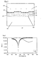
-
Figur 1 zeigt schematisch eine Struktur gemäß dem Stand der Technik gemäß der Novartis Anmeldung. Zusätzlich zeigt die Figur die in dieser Struktur sich aufbauende Feldverteilung bei Beaufschlagung mit Licht. -
Figur 2 zeigt die mit der inFigur 1 verbundene Abhängigkeit der Reflexion und der Transmission als Funktion der Wellenlänge. Deutlich sichtbar ist die anomale Reduktion der Transmission auf kleiner 1%. - -
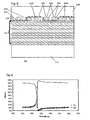
Figur 3 zeigt schematisch eine Ausführungsform einer Struktur gemäß der vorliegenden Erfindung. Zusätzlich zeigt die Figur sich aufbauende Feldverteilung bei Beaufschlagung mit Licht. -
Figur 4 zeigt die mit dem inFigur 3 dargestellten System verbundene Abhängigkeit der Reflexion und der Transmission als Funktion der Wellenlänge. Die Spektren weisen weder anomale Reflexion noch anomale Transmission auf. -
Figur 5 -
Figur 6 zeigt die mit dem inFigur 5 -
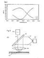
Figur 7 zeigt den zuFigur 6 analogen Graphen für den Bereich von 632.8nm bis 633.2nm. Hierbei wird deutlich, dass bei einer Wellenlänge von 632.95nm die Reflexion sogar ganz unterdrückt werden kann. -
Figur 8 zeigt einen Messaufbau gemäß der vorliegenden Erfindung zur selektiven Detektion von Messsubstanzen. - Die Erfindung wird im folgenden detailliert mit Hilfe von Beispielen und anhand der Figuren beschrieben.
-
FIG. 1 schematically shows a structure according to the prior art according to the Novartis application. In addition, the figure shows the field distribution in this structure when exposed to light. -
FIG. 2 shows the with the inFIG. 1 Associated dependence of reflection and transmission as a function of wavelength. Clearly visible is the anomalous reduction of the transmission to less than 1%. - -
FIG. 3 schematically shows an embodiment of a structure according to the present invention. In addition, the figure shows an expanding field distribution when exposed to light. -
FIG. 4 shows the with the inFIG. 3 illustrated system dependent reflection and transmission as a function of wavelength. The spectra show neither abnormal reflection nor abnormal transmission. -
FIG. 5 schematically shows a further advantageous embodiment of a structure according to the present invention. -
FIG. 6 shows the with the inFIG. 5 illustrated linked dependence of reflection and transmission as a function of wavelength. It can be clearly seen that the reflectance drops below 1%. -
FIG. 7 shows that tooFIG. 6 analogue graph for the range from 632.8nm to 633.2nm. It becomes clear that with a wavelength of 632.95nm the reflection can even be completely suppressed. -
FIG. 8 shows a measuring structure according to the present invention for the selective detection of measuring substances. - The invention will be described in detail below with the aid of examples and with reference to the figures.
Um die Grundidee der vorliegenden Erfindung besser verständlich zu machen ist es hilfreich zunächst ein typisches Beispiel des Stand der Technik wie es in der Novartis-Anmeldung offenbart ist, genauer zu analysieren. Ein solches System 97 ist in
Das System wird im Beispiel mit Licht der Wellenlänge 633nm unter einem Einfallswinkel von ϑ1=2.9° mit TE-Polarisation beaufschlagt. Dieser Winkel entspricht dem Resonanzwinkel des Systems bei dem die Transmission anormal reduziert ist. Die Beaufschlagung erfolgt von der Superstratseite aus. Der einfallende Lichtstrahl spannt zusammen mit der Flächennormalen auf die hochbrechende Schicht die Einfallsebene auf. Die Beaufschlagung erfolgt derart, dass die Gitterstege diese Einfallsebene senkrecht durchstoßen, das heißt im hier betrachteten Beispiel handelt es sich um nicht konische Beaufschlagung. Die TE-Polarisation ist dadurch gekennzeichnet, dass dabei der elektrische Feldvektor in der Ebene senkrecht zur Einfallsebene schwingt.In the example, the system is subjected to TE polarization with light of wavelength 633 nm under an incident angle of θ 1 = 2.9 °. This angle corresponds to the resonance angle of the Systems where the transmission is abnormally reduced. The admission takes place from the Superstratseite. The incident light beam, together with the surface normal to the high refractive layer, spans the plane of incidence. The loading is carried out in such a way that the grid webs pierce this plane of incidence perpendicular, that is, in the example considered here is not conical loading. The TE polarization is characterized in that the electric field vector oscillates in the plane perpendicular to the plane of incidence.
In der
Betrachtet man hier die Beugungseffizienzen als Funktion der Wellenlänge, dargestellt in
Im ersten Beispiel gemäß der vorliegenden Erfindung, schematisch in
Das System wird im Beispiel mit Licht der Wellenlänge 633nm unter einem Einfallswinkel von ϑ=2° mit TE-Polarisation beaufschlagt. Die Beaufschlagung erfolgt von der Superstratseite aus. Der einfallende Lichtstrahl spannt zusammen mit der Flächennormalen auf die letzte Schicht die Einfallsebene auf. Die Beaufschlagung erfolgt derart, dass die Gitterstege diese Einfallsebene senkrecht durchstoßen, das heißt im hier betrachteten Beispiel handelt es sich um nicht konischen Einfall. Die TE-Polarisation ist dadurch gekennzeichnet, dass dabei der elektrische Feldvektor in der Ebene senkrecht zur Einfallsebene schwingt. Damit ist die Beaufschlagungsbedingung mit Licht bis auf den geänderten Einfallswinkel identisch zum erläuterten Beispiel des Stand der Technik.In the example, the system is subjected to TE polarization with light of wavelength 633 nm under an angle of incidence of θ = 2 °. The admission takes place from the Superstratseite. The incident light beam, together with the surface normal to the last layer, spans the plane of incidence. The loading is carried out in such a way that the grid webs pierce this plane of incidence perpendicular, that is, in the example considered here is not conical incidence. The TE polarization is characterized in that the electric field vector oscillates in the plane perpendicular to the plane of incidence. Thus, the loading condition with light is identical except for the changed angle of incidence to the explained example of the prior art.
Zur vollständigen Definition des Systems fehlen lediglich noch die Schichtdicken der einzelnen Schichten, sowie die Gittertiefe der Gitterstruktur. Diese wurden mit Hilfe von statistischer Optimierung aufgefunden. Hinsichtlich der Zielfunktion für die Optimierung gibt es unterschiedliche Möglichkeiten. Im Beispiel wurde als Ziel der Optimierung die maximale Feldstärke an einer Stelle im Bereich innerhalb der Gittergräben definiert. Zur Optimierung eignen sich sowohl lokale Optimierungsmethoden als auch globale Methoden, die beide dem Fachmann z.B. für die Optimierung von optischen Wechselschichtsystemen in der Dünnfilmtechnik hinreichend bekannt sind. Die Anwendung solcher Optimierungsmethoden im Zusammenhang mit der vorliegenden Anwendung ist dagegen neu und erfinderisch. Allerdings weiß der Fachmann, wie vorzugehen ist, sobald ihm der neue Aspekt offenbart wurde, dass er die Feldstärke optimieren soll und diesbezüglich die Systemparameter als Optimierungsparameter, insbesondere die Schichtdicken und die Gittertiefe ansetzen soll. Damit ist die Lehre zum technischen Handeln vollständig offenbart.For a complete definition of the system, only the layer thicknesses of the individual layers and the grid depth of the lattice structure are missing. These were found by means of statistical optimization. There are various possibilities with regard to the objective function for the optimization. In the example, the goal of the optimization was the maximum field strength defined at a location in the area within the grid trenches. For optimization, both local optimization methods and global methods are suitable, both of which are well known to the person skilled in the art, for example for the optimization of optical alternating-layer systems in thin-film technology. The use of such optimization methods in connection with the present application, however, is new and inventive. However, the skilled person knows how to proceed, as soon as the new aspect has been revealed to him, that he should optimize the field strength and, in this regard, set the system parameters as optimization parameters, in particular the layer thicknesses and the grid depth. This completely reveals the doctrine of technical action.
Die folgende Tabelle 1 zeigt das Resultat einer solchen Optimierung:
In der
Wie aus der
Der aus dem Stand der Technik bekannte Effekt der resonanten Gitter, der zu einer anormalen Reduktion der Transmission führt, geht, wie beschrieben, einher mit einer Reflexion von nahezu 100%. In
In folgenden zweiten Beispiel wird sogar erreicht dass die Reflexion des Systems auf unter 10% sinkt. Wiederum umfaßt das System 211 ein Substrat 223, ein Schichtsystem 227, einen Gitterbereich 229 mit einer Periode von 550nm, biologische Koppelelemente 233,233',233'' und ein Superstrat 239. Die Art des beaufschlagten Lichtes entspricht der Art des ersten Beispiels. Es wurde bei der Optimierung als Ziel die Anforderung gestellt, die Reflexion entsprechend niedrig zu halten bei immer noch hoher Feldstärke in den Gittergräben. Das System wurde entsprechend dem im ersten Beispiel beschriebenen System angesetzt, wobei hier 16 Schichten für die Optimierung angesetzt wurden und anstatt TiO2-Schichten wurden Ta2O5-Schichten verwendet. Die Optimierung der Schichtdicken ergab das folgende System:
Die
Wie zu sehen ist eine hohe Feldstärke im Bereich der Gittergräben realisiert.The
As can be seen, a high field strength is realized in the region of the grid trenches.
Die dazugehörende
Die
Natürlich gibt es unterschiedliche Ausgestaltungsformen einer solchen Anordnung. Zum Beispiel kann man eine Lichtquelle verwenden, die die Linse 331 gleichzeitig mit unterschiedlichen diskreten oder kontinuierlichen Winkeln beaufschlagt und somit mehrere Punkte oder einen ganzen Bereich der Oberfläche des Messchips 311 beleuchtet. Wird dann anstatt des Detektors eine Detektorzeile oder Matrix verwendet (zum Beispiel ein CCD-Chip) so können gleichzeitig mehrere Bereiche des Messchips ausgewertet werden.Of course, there are different embodiments of such an arrangement. For example, one may use a light source which simultaneously exposes the
In der Regel werden die zu messenden Substanzen gelöst in einer flüssigen Probe auf das Substrat aufgebracht. Dabei ist es wichtig, dass eine geringe Ausdehnung der Tropfen auf der Oberfläche realisiert werden kann. Es hat sich gezeigt, dass insbesondere bei tiefen Gittergräben die Tropfen dazu tendieren auseinander zu laufen. Dies aufgrund der durch die Gräben auf die Tropfen wirkenden Kapillarkräfte. Im Extremfall fliesen die Tropfen sogar ineinander über. Um dem entgegen zu wirken können die Gräben durch Fliessbarrieren verstopft werden. Dies können beispielsweise zu den Gitterstäben quer stehende , durchgehende Wände sein. Solche Wände lassen sich durch dielektrisches Beschichten der Plattform durch eine Maske hindurch realisieren. Typische Größen für die Durchmesser einzelner Messfelder, im folgenden Spot-Durchmesser genannt, sind derzeit 80µm bis 200µm. Vorteilhafterweise ist der Abstand zweier Wände jedoch mindestens Faktor drei kleiner, vorzugsweise Faktor fünf bis zehn kleiner als der zu erreichende Spot-Durchmesser damit garantiert ist, dass tatsächlich nicht zwei Tropfen sich einen gleichen Zwischenwandbereich teilen müssen.In general, the substances to be measured are applied dissolved in a liquid sample on the substrate. It is important that a small extent of the drops on the surface can be realized. It has been found that, especially with deep trenches, the drops tend to diverge. This is due to the capillary forces acting on the drops through the trenches. In extreme cases, the drops even overlap. To counteract this, the trenches can be blocked by flow barriers. This can be, for example, to the bars transverse, continuous walls. Such walls can be realized by dielectrically coating the platform through a mask. Typical sizes for the diameters of individual measuring fields, referred to below as the spot diameter, are currently 80 μm to 200 μm. Advantageously, however, the distance between two walls is at least a factor of three smaller, preferably a factor of five to ten smaller than the spot diameter to be achieved, so that in fact not two drops must share a same intermediate wall area.
Bisher wurden lediglich die Methoden zur Messung von sich spezifisch bindenden Substanzen betrachtet, die auf der Basis von Fluoreszenzmarken arbeiten. Es ist jedoch klar, dass das erfindungsgemäße System auch direkte Messmethoden ermöglicht, d.h. Messmethoden die ohne spezifischen Marker auskommen. Eine ausführliche Beschreibung solcher Label-freien Methoden ist zum Beispiel in
Label-freie, selektive Messung wird zum Beispiel durch spezifische Chemisorption oder Physisorption, Adsorption, Desorption und/oder chemische Bindung (im folgenden unter Substanzeinwirkung zusammengefasst) von zu messenden Substanzen an der Oberfläche möglich. Dies führt zu einer messbaren Veränderung der Konfiguration des die Feldverteilung mitbestimmenden Gesamtlayouts des Messchips und insbesondere die des Gitterbereichs. Beispielsweise kann sich durch eine solche Substanzeinwirkung der Füllfaktor des Gitterbereichs ändern, der aber entscheidend die Beugungseffizienzen mitbeeinflusst. Es ist klar, dass Selektivität einer solchen Substanzeinwirkung auch mittels einer Zusatzschicht erzielt werden kann, die aufgrund des sogenannten Schlüssel-Schloss-Prinzips die zu messenden Substanzen spezifisch an sich bindet. Zum Beispiel könnten zu Messbeginn lediglich Antikörper an der Gitteroberfläche, insbesondere den Gittergräben folgend, gebunden sein. Während der Messung binden sich die entsprechenden Antigene und ändern dadurch die Gitterkonfiguration.Label-free, selective measurement is possible, for example, by specific chemisorption or physisorption, adsorption, desorption and / or chemical bonding (summarized below under the influence of substances) of substances to be measured on the surface. This leads to a measurable change in the configuration of the overall distribution of the measuring chip, which determines the field distribution, and in particular that of the grid region. For example, such a substance effect may change the fill factor of the grating region, which, however, decisively influences the diffraction efficiencies. It is clear that selectivity of such a substance effect can also be achieved by means of an additional layer which specifically binds the substances to be measured on the basis of the so-called key-lock principle. For example, at the beginning of the measurement, only antibodies could be bound to the lattice surface, in particular following the lattice trenches. During the measurement, the corresponding antigens bind and thereby change the lattice configuration.
Besonders interessant ist die Möglichkeit, auf die erfindungsgemäßen Systeme einen Filter direkt zu integrieren. Es ist nämlich möglich, die Gitterstrukturen so zu beschichten, dass die Gittergräben nicht oder nur wenig gefüllt werden, während sich Schichtmaterial im wesentlichen auf den Gitterstegen ablagert. Dies kann beispielsweise durch Beschichten mittels Sputtertechniken erzielt werden. Bei diesem Beschichtungsprozess verjüngt sich mit zunehmender Beschichtungsdicke der Gittergraben. Es entsteht daher ein sich zur Oberfläche hin verjüngender Kanal, d.h. mittels Beschichtung kann jede gewünschte Öffnungsbreite, die kleiner oder gleich der ursprünglichen Grabenbreite ist, eingestellt werden. Partikel, die sich in der Messsubstanz befinden und einen größeren Durchmesser als die Kanalbreite haben, werden nicht in die Grabenregion diffundieren können. Damit liegt die Möglichkeit einer integrierten mechanischen Filterung vor. Es besteht die Möglichkeit den sich verjüngenden Kanal aus einem Wechselschichtsystem aufzubauen, dessen Material und Schichtdickenverteilung im Hinblick auf optische Anforderungen optimiert werden können.Of particular interest is the possibility of directly integrating a filter on the systems according to the invention. Namely, it is possible to coat the lattice structures so that the lattice trenches are not or only slightly filled, while layer material is deposited substantially on the lattice webs. This can be achieved, for example, by coating using sputtering techniques. In this coating process, the lattice trench tapers with increasing coating thickness. There is therefore a channel tapering towards the surface, i. By means of coating, any desired opening width, which is smaller than or equal to the original trench width, can be set. Particles that are in the measurement substance and have a larger diameter than the channel width will not be able to diffuse into the trench region. This provides the possibility of integrated mechanical filtering. It is possible to build the tapered channel from a alternating layer system whose material and layer thickness distribution can be optimized with respect to optical requirements.
In
Es wurden unterschiedliche Ausführungsformen von erfindungsgemäßen Systemen beschrieben. Um die dafür notwendigen Schichtsysteme herzustellen, können die unterschiedlichen und dem Fachmann geläufigen Beschichtungsverfahren, wie zum Beispiel thermisch bedampfen, PVD, CVD, insbesondere PECVD oder PICVD und andere verwendet werden. Zur Herstellung des Gitterbereichs eignen sich Interferenzverfahren, insbesondere Verfahren, die auf der Belichtung einer photoempfindlichen Schicht mittels Zweistrahlinterferenz beruhen oder Phasenmasken ausnutzen. Anschließend werden mittels der bekannten Lithographietechniken die in der photoempfindlichen Schicht realisierten Gitterstrukturen in die darunter liegende Schicht übertragen.Different embodiments of systems according to the invention have been described. To the necessary Layer systems, the different and familiar to those skilled coating methods, such as thermal evaporation, PVD, CVD, in particular PECVD or PICVD and others can be used. Interference methods, in particular methods which are based on the exposure of a photosensitive layer by means of two-beam interference or utilize phase masks, are suitable for the production of the grating region. Subsequently, by means of the known lithographic techniques, the grating structures realized in the photosensitive layer are transferred into the underlying layer.
Eine Schwierigkeit kann darin bestehen, dass das unter dem Gitterbereich liegende Schichtsystem die Belichtung zur Herstellung des Gitters stört. In diesem Fall kann es von Vorteil sein, auf eine Prägetechnik umzusteigen, bei dem beispielsweise ein Polymer auf das Schichtsystem aufgebracht wird, dem anschließend mittels eines Prägestempels ein Gitter aufgeprägt wird. Mittels der nachfolgenden Lithographie wird dann das Gitter in die darunter liegende Schicht übertragen. Eine andere Möglichkeit diese Schwierigkeit zu umgehen besteht darin, ein erfindungsgemäßes System zu wählen, bei dem das Gitter im Substrat realisiert ist und sich die Gitterstrukturen bis an die Oberfläche übertragen. Auch eine solche Ausführungsform lässt die Möglichkeit zu, erfindungsgemäß den wesentlichen Anteil des sich aufbauenden elektromagnetischen Feldes in der Gitterstruktur und dabei unter anderem in den für die Messsubstanzen zugänglichen Gittergräben zu konzentrieren.One difficulty may be that the layer system below the grating area interferes with the exposure for making the grating. In this case, it may be advantageous to switch to an embossing technique in which, for example, a polymer is applied to the layer system, which is then impressed by means of a stamping die a grid. By means of the following lithography, the grating is then transferred to the underlying layer. Another way around this difficulty is to choose a system according to the invention, in which the grid is realized in the substrate and transfer the grid structures to the surface. Such an embodiment also makes it possible to concentrate according to the invention the essential portion of the electromagnetic field which builds up in the lattice structure and, inter alia, in the lattice trenches accessible for the measuring substances.
Die hier besprochenen Ausführungsformen der Erfindung sind lediglich als Beispiele anzusehen auf die der Gegenstand der Erfindung jedoch nicht beschränkt ist. Es sind beispielsweise unterschiedlichste Varianten der Ausführung der Beleuchtung denkbar:
- In den Beispielen wurde durchweg TE-polarisiertes Licht verwendet, wobei sich der Gegenstand der Erfindung auch auf Beaufschlagung mit TM-polarisiertem Licht erstrecken soll.
- In den Beispielen wurde lediglich nicht-konische Beaufschlagung mit Licht betrachtet. Es ist aber auch möglich Konfigurationen mit konischer Beaufschlagung zu wählen.
- Es sind Ausführungsformen denkbar, die kohärentes, inkohärentes oder teilkohärentes Licht verwenden.
- Es sind erfindungsgemäße Ausführungsformen mit polarisiertem Licht oder mit unpolarisiertem Licht denkbar. Bei speziell gewählter Polarisation, beispielsweise bei zirkularer Polarisation sind z.B Messungen der Phasenverschiebung und insbesondere der Änderung der Phasenverschiebung möglich.
- Als Lichtquellen kommen breitbandige Lichtquellen und/oder schmalbandige Lichtquellen und/oder monochromatische Lichtquellen in Frage. D.h. möglich ist unter anderem der Einsatz von kontinuierlichen oder gepulsten Lasern, insbesondere Halbleiterlasern, Leuchtdioden (LED) und Glühlampen.
- In the examples, TE polarized light was used throughout, and the subject invention is also intended to extend to exposure to TM polarized light.
- In the examples, only non-conical light exposure was considered. But it is also possible to choose configurations with conical admission.
- Embodiments are conceivable which use coherent, incoherent or partially coherent light.
- Embodiments according to the invention with polarized light or with unpolarized light are conceivable. With specially selected polarization, for example in the case of circular polarization, it is possible, for example, to measure the phase shift and in particular the change in the phase shift.
- Suitable light sources are broadband light sources and / or narrowband light sources and / or monochromatic light sources. That is possible, inter alia, the use of continuous or pulsed lasers, in particular semiconductor lasers, light emitting diodes (LED) and incandescent lamps.
Das zur Beaufschlagung verwendete Licht kann aus unterschiedlichen Richtungen kommen:
- Substratseitig
- Superstratseitig
- über ein im erfindungsgemäßen System zusätzlich integrierten und möglicherweise strukturierten Wellenleiter oder aus einer Kombination einzelner oder mehrerer oder aller.
- the substrate side
- Superstrate side
- via an additionally integrated and possibly structured waveguide in the system according to the invention or from a combination of one or more or all.
Es wurden hier lediglich Gitterbereiche beschrieben, die eindimensionale, rechteckige Gitterprofile aufweisen. Auch hier sind erfindungsgemäße Ausführungsformen möglich und Gegenstand der vorliegenden Erfindung, die sich auf allgemeinere Gitterstrukturen beziehen. Beispielsweise:
- Eindimensionale Gitter, deren Profil von der Rechteckform abweicht und/oder deren Füllfaktoren von 0.5 abweichen.
- Eindimensionale Gitter, bei denen zwei oder mehrere Gitterperioden überlagert sind, deren Gittervektoren parallel zueinander sind.
- Zweidimensionale Gitter, d.h. periodische Strukturen mit mindestens zwei nicht parallelen Gittervektoren (gekreuzte Gitter), wobei insbesondere diejenigen zweidimensionalen Gitter in Bezug auf Polarisationseffekte interessant sind, deren Gittervektoren senkrecht aufeinander stehen und/oder betrags-mäßig gleich sind.
- Periodische Strukturen, die selbst aus Schichtsystemen aufgebaut sind.
- One-dimensional lattice whose profile deviates from the rectangular shape and / or whose fill factors deviate from 0.5.
- One-dimensional grids in which two or more grating periods are superimposed whose grating vectors are parallel to each other.
- Two-dimensional lattices, ie periodic structures with at least two non-parallel lattice vectors (crossed lattices), in particular those two-dimensional lattices in With respect to polarization effects are interesting whose lattice vectors are perpendicular to each other and / or equal in terms of magnitude.
- Periodic structures, which themselves are composed of layer systems.
Als Teilaspekt der hier beschriebenen Erfindung wurde bereits beschrieben, dass es möglich ist die hohe Feldverteilung in einem Gitterbereich zu konzentrieren, in dem die Brechungsindizes der beteiligten Materialien gleich oder kleiner als der Brechungsindex des Substrates ist.As a partial aspect of the invention described herein it has already been described that it is possible to concentrate the high field distribution in a grating region in which the refractive indices of the materials involved are equal to or smaller than the refractive index of the substrate.
Ein anderer Teilaspekt der Erfindung ist die Möglichkeit, dass aufgrund der Gittergräben den zu messenden Substanzen Bereiche maximaler Feldstärke zugänglich sind. Dieser erfinderische Aspekt kann auch durch einen strukturierten Gitterbereich erzielt werden, bei dem eines oder mehrere der beteiligten Materialen einen Brechungsindex besitzt der über dem Brechungsindex des Substrates liegt.Another aspect of the invention is the possibility that, due to the grid trenches, areas of maximum field strength are accessible to the substances to be measured. This inventive aspect can also be achieved by a structured grating region in which one or more of the involved materials has a refractive index which is above the refractive index of the substrate.
In den Beispielen wurden lediglich Systeme beschrieben, die die erfindungsgemäßen Effekte ausschließlich mittels dielektrischer Materialien erzielen. Es sind aber auch erfindungsgemäße Ausführungsformen möglich, die metallische Materialien und insbesondere strukturierte metallische Materialien umfassen. Weiterhin sind Ausführungsformen möglich, die die erfindungsgemäßen Effekte (hohes Feld in den für Messsubstanzen zugänglichen Gittergräben) mit den aus dem Stand der Technik bekannten Effekten, insbesondere mit Oberflächenplasmonen kombinieren.In the examples, only systems were described which achieve the effects according to the invention exclusively by means of dielectric materials. However, embodiments according to the invention are also possible which comprise metallic materials and in particular structured metallic materials. Furthermore, embodiments are possible which combine the effects according to the invention (high field in the grating trenches accessible for measuring substances) with the effects known from the prior art, in particular with surface plasmons.
Der Schwerpunkt in der Beschreibung war die Verwendung eines erfindungsgemäßen Systems in der Sensorik. Das erfindungsgemäße System ist allerdings immer dort anwendbar, wo im Nahfeld (d.h. im Bereich von bis zu ca 10 Wellenlängen Abstand von der Oberfläche) Substanzen belichtet werden sollen. Die Tatsache, dass beispielsweise im System in 
- 97
- System
- 101
- Substrat
- 103
- Periodisches Gitter
- 107
- Dielektrische Schicht
- 109
- Biologische Koppelelemente
- 113
- Superstrat
- 11
- System
- 13
- Substrat
- 17
- Schichtsystem ,
- 19
- Gitterstruktur
- 23
- Gitterstege
- 29
- Gittergräben
- 31
- Biologische Koppelelemente am Grabenboden
- 31'
- Biologische Koppelelemente an den Seitenwänden
- 31''
- Biologische Koppelelemente auf den Gitterstäben
- 37
- Superstrat
- 211
- System
- 223
- Substrat
- 227
- Schichtsystem
- 229
- Gitterbereich
- 233
- Biologische Bindungsmoleküle am Grabenboden
- 233'
- Biologische Bindungsmoleküle an den Seitenwänden
- 233''
- Biologische Bindungsmoleküle auf den Gitterstäben
- 239
- Superstrat
- 307
- Messaufbau
- 311
- Messchip
- 313
- Lichtquelle
- 317
- Selektiver Spiegel
- 331
- Linse
- 337
- Detektor
- LA
- Anregungslicht
- LF
- Fluoreszenzlicht
- 5
- Linie gleichen
Amplitudenquadrats mit Wert 5 - 10
- Linie gleichen
Amplitudenquadrats mit Wert 10 - 15
- Linie gleichen
Amplitudenquadrats mit Wert 15 - 20
- Linie gleichen
Amplitudenquadrats mit Wert 20
- 50
- Linie gleichen
Amplitudenquadrats mit Wert 50 - 100
- Linie gleichen
Amplitudenquadrats mit Wert 100 - 150
- Linie gleichen
Amplitudenquadrats mit Wert 150 - 200
- Linie gleichen
Amplitudenquadrats mit Wert 200
- 250
- Linie gleichen
Amplitudenquadrats mit Wert 250 - 500
- Linie gleichen
Amplitudenquadrats mit Wert 500 - 750
- Linie gleichen
Amplitudenquadrats mit Wert 750 - 1000
- Linie gleichen
Amplitudenquadrats mit Wert 1000
- 97
- system
- 101
- substratum
- 103
- Periodic grid
- 107
- Dielectric layer
- 109
- Biological coupling elements
- 113
- superstrate
- 11
- system
- 13
- substratum
- 17
- Layer system,
- 19
- lattice structure
- 23
- grid webs
- 29
- grid trenches
- 31
- Biological coupling elements at the trench bottom
- 31 '
- Biological coupling elements on the side walls
- 31 ''
- Biological coupling elements on the bars
- 37
- superstrate
- 211
- system
- 223
- substratum
- 227
- layer system
- 229
- grating region
- 233
- Biological binding molecules at the trench bottom
- 233 '
- Biological binding molecules on the sidewalls
- 233 ''
- Biological binding molecules on the bars
- 239
- superstrate
- 307
- measurement setup
- 311
- measuring chip
- 313
- light source
- 317
- Selective mirror
- 331
- lens
- 337
- detector
- LA
- excitation light
- LF
- fluorescent light
- 5
- Line of equal amplitude square with
value 5 - 10
- Line of equal amplitude square with
value 10 - 15
- Line of equal amplitude square with
value 15 - 20
- Line of equal amplitude square with
value 20
- 50
- Line of equal amplitude square with
value 50 - 100
- Line of equal amplitude square with
value 100 - 150
- Line of equal amplitude square with
value 150 - 200
- Line of equal amplitude square with
value 200
- 250
- Line of equal amplitude square with
value 250 - 500
- Line of equal amplitude square with
value 500 - 750
- Line of equal amplitude square with
value 750 - 1000
- Line of equal amplitude square with
value 1000
Claims (11)
- Platform to generate an electromagnetic field distribution, with- a substrate (13)- a structured layer (19) provided on the substrate, wherein the layer thickness of the structured layer (19) is determined by the maximum structure depth,- coupling means (23, 29) to couple the impacted electromagnetic radiation into the structured layer to create an electromagnetic field distribution within the structured layer (19), characterised in that between the substrate (13) and the structured layer (19) is provided a multilayer system such that the multilayer system (17) at least partly prevents electromagnetic fields that are created in the structured layer (19) coupling to those of higher diffractive orders of the fields differing from zero which propagate in the substrate (13),wherein the structured layer (19), the coupling means (23, 29) and the multilayer system (17) are matched to each other so that on suitable impacting of the platform with electromagnetic radiation, the maximum field intensity of the created electromagnetic field intensities lies in the area of the structured layer (19).
- Platform according to claim 1, characterised in that the refractive index or where applicable the effective refractive index of the structured layer (19) is less than 1% higher, preferably lower than the refractive index of the substrate (13).
- Platform according to any of claims 1 and 2, characterised in that the structure of the structured layer (19) substantially comprises periodically arranged recesses (29) which are a constituent part of the coupling means.
- Platform according to any of the preceding claims, characterised in that the multilayer system (17) comprises metallic layers, preferably of Al and/or Ag.
- Platform according to any of claims 1 to 3, characterised in that the multilayer system (17) comprises dielectric layers and preferably no metallic layers, wherein the layer system is preferably constructed in alternating layer structure in which high and low refractive layers are arranged alternately.
- Platform according to claims 1 to 5, characterised in that the nature of the structuring, the coupling means (23, 29) and the number, material and thickness distribution of the layers of the multilayer system are selected such that the field intensity distribution generated on suitable impacting of the platform with electromagnetic radiation has at least one maximum in the areas (29) free from layer material in the structured layer (19).
- Field distribution platform which comprises a platform according to any of claims 1 to 6, with a source for generating electromagnetic radiation and with an electromagnetic field, the field strength of which is at a maximum in the area of the structured layer.
- Field distribution platform which comprises a platform according to any of claims 1 to 7, characterised in that the electromagnetic field distribution has at least one maximum in the areas (29) free from layer material in the structured layer (19).
- Sensor with a platform or a field distribution platform according to any of the preceding claims to measure specific substances in a biological and/or chemical and/or biochemical specimen.
- Method for generating a raised, not exclusively evanescent electromagnetic field distribution with the following steps:- selection of a substrate (13)- selection of a material and the structure of a structured layer- selection of materials for a multilayer system- establishing of parameters of an electromagnetic radiation to be used for impacting- simulation and optimisation of the electromagnetic field distribution within a platform comprising the substrate, the multilayer system and the structured layer on impacting with electromagnetic radiation according to the established parameters,wherein the multilayer system is provided between the substrate and the structured layer, and at least partly prevents electromagnetic fields that are created in the structured layer (19) coupling to those of higher diffractive orders of the fields differing from zero which propagate in the substrate (13), and the maximum field intensity at a point within the structured layer is defined as the optimization target;- creation of the platform at least approximately according to the results of optimisation;impacting of the platform with electromagnetic radiation according to the established parameters.
- Method according to claim 10, characterised in that as an optimisation target, an electromagnetic field distribution is desired which has at least one maximum in the areas which are free from layer material in the structured layer.
Applications Claiming Priority (3)
| Application Number | Priority Date | Filing Date | Title |
|---|---|---|---|
| US43498702P | 2002-12-19 | 2002-12-19 | |
| US434987P | 2002-12-19 | ||
| PCT/CH2003/000811 WO2004057315A1 (en) | 2002-12-19 | 2003-12-11 | Method for generating electromagnetic field distributions |
Publications (2)
| Publication Number | Publication Date |
|---|---|
| EP1576356A1 EP1576356A1 (en) | 2005-09-21 |
| EP1576356B1 true EP1576356B1 (en) | 2009-10-28 |
Family
ID=32682135
Family Applications (1)
| Application Number | Title | Priority Date | Filing Date |
|---|---|---|---|
| EP03775037A Expired - Lifetime EP1576356B1 (en) | 2002-12-19 | 2003-12-11 | Apparatus and method for generating electromagnetic field distributions |
Country Status (9)
| Country | Link |
|---|---|
| US (1) | US7110181B2 (en) |
| EP (1) | EP1576356B1 (en) |
| KR (1) | KR20050084016A (en) |
| CN (1) | CN100585384C (en) |
| AT (1) | ATE447171T1 (en) |
| AU (1) | AU2003283175A1 (en) |
| DE (1) | DE50312077D1 (en) |
| TW (1) | TWI322264B (en) |
| WO (1) | WO2004057315A1 (en) |
Families Citing this family (29)
| Publication number | Priority date | Publication date | Assignee | Title |
|---|---|---|---|---|
| US5914613A (en) | 1996-08-08 | 1999-06-22 | Cascade Microtech, Inc. | Membrane probing system with local contact scrub |
| US6256882B1 (en) | 1998-07-14 | 2001-07-10 | Cascade Microtech, Inc. | Membrane probing system |
| US6965226B2 (en) | 2000-09-05 | 2005-11-15 | Cascade Microtech, Inc. | Chuck for holding a device under test |
| US6914423B2 (en) | 2000-09-05 | 2005-07-05 | Cascade Microtech, Inc. | Probe station |
| DE20114544U1 (en) | 2000-12-04 | 2002-02-21 | Cascade Microtech Inc | wafer probe |
| AU2002327490A1 (en) | 2001-08-21 | 2003-06-30 | Cascade Microtech, Inc. | Membrane probing system |
| US7863052B2 (en) * | 2005-08-11 | 2011-01-04 | Sru Biosystems, Inc. | Grating-based sensor combining label-free binding detection and fluorescence amplification and readout system for sensor |
| US7057404B2 (en) | 2003-05-23 | 2006-06-06 | Sharp Laboratories Of America, Inc. | Shielded probe for testing a device under test |
| US7492172B2 (en) | 2003-05-23 | 2009-02-17 | Cascade Microtech, Inc. | Chuck for holding a device under test |
| US7250626B2 (en) | 2003-10-22 | 2007-07-31 | Cascade Microtech, Inc. | Probe testing structure |
| US7187188B2 (en) | 2003-12-24 | 2007-03-06 | Cascade Microtech, Inc. | Chuck with integrated wafer support |
| DE202004021093U1 (en) | 2003-12-24 | 2006-09-28 | Cascade Microtech, Inc., Beaverton | Differential probe for e.g. integrated circuit, has elongate probing units interconnected to respective active circuits that are interconnected to substrate by respective pair of flexible interconnects |
| KR20070058522A (en) | 2004-09-13 | 2007-06-08 | 캐스케이드 마이크로테크 인코포레이티드 | Double sided probing structures |
| US7535247B2 (en) | 2005-01-31 | 2009-05-19 | Cascade Microtech, Inc. | Interface for testing semiconductors |
| US7656172B2 (en) | 2005-01-31 | 2010-02-02 | Cascade Microtech, Inc. | System for testing semiconductors |
| US7790406B2 (en) * | 2005-08-11 | 2010-09-07 | Sru Biosystems, Inc | Grating-based sensor combining label-free binding detection and fluorescence amplification and readout system for sensor |
| US7764072B2 (en) | 2006-06-12 | 2010-07-27 | Cascade Microtech, Inc. | Differential signal probing system |
| US7403028B2 (en) | 2006-06-12 | 2008-07-22 | Cascade Microtech, Inc. | Test structure and probe for differential signals |
| US7723999B2 (en) | 2006-06-12 | 2010-05-25 | Cascade Microtech, Inc. | Calibration structures for differential signal probing |
| US20080012578A1 (en) * | 2006-07-14 | 2008-01-17 | Cascade Microtech, Inc. | System for detecting molecular structure and events |
| WO2008010182A2 (en) * | 2006-07-17 | 2008-01-24 | Max Wiki | Analytical system comprising an arrangement for temporally variable spatial light modulation and detection method implemented thereby |
| US7876114B2 (en) | 2007-08-08 | 2011-01-25 | Cascade Microtech, Inc. | Differential waveguide probe |
| EP2060904A1 (en) * | 2007-11-13 | 2009-05-20 | Koninklijke Philips Electronics N.V. | Plasmon grating biosensor |
| US7888957B2 (en) | 2008-10-06 | 2011-02-15 | Cascade Microtech, Inc. | Probing apparatus with impedance optimized interface |
| WO2010059247A2 (en) | 2008-11-21 | 2010-05-27 | Cascade Microtech, Inc. | Replaceable coupon for a probing apparatus |
| US8319503B2 (en) | 2008-11-24 | 2012-11-27 | Cascade Microtech, Inc. | Test apparatus for measuring a characteristic of a device under test |
| EP2221605A1 (en) * | 2009-02-12 | 2010-08-25 | Koninklijke Philips Electronics N.V. | A wire grid sensor |
| FR2954524B1 (en) * | 2009-12-17 | 2012-09-28 | Ecole Polytech | OPTIMIZED DIELECTRIC REFLECTING DIFFRACTION NETWORK |
| TWI571648B (en) * | 2016-01-26 | 2017-02-21 | 國立彰化師範大學 | System for detecting megnetic field distribution |
Family Cites Families (6)
| Publication number | Priority date | Publication date | Assignee | Title |
|---|---|---|---|---|
| GB2256477B (en) * | 1991-06-07 | 1995-03-08 | Marconi Gec Ltd | An optical sensor |
| US5907436A (en) * | 1995-09-29 | 1999-05-25 | The Regents Of The University Of California | Multilayer dielectric diffraction gratings |
| DE69722008T2 (en) * | 1996-08-21 | 2004-04-01 | Polaroid Corp., Waltham | SYSTEMS AND METHODS BASED ON PHASE CONTROLLING FIELDS |
| GB9803704D0 (en) * | 1998-02-24 | 1998-04-15 | Univ Manchester | Waveguide structure |
| EP1272829A1 (en) * | 2000-04-14 | 2003-01-08 | Zeptosens AG | Grid-waveguide structure for reinforcing an excitation field and use thereof |
| WO2002008810A2 (en) * | 2000-07-21 | 2002-01-31 | Micro Managed Photons A/S | Surface plasmon polariton band gap structures |
-
2003
- 2003-12-11 EP EP03775037A patent/EP1576356B1/en not_active Expired - Lifetime
- 2003-12-11 WO PCT/CH2003/000811 patent/WO2004057315A1/en not_active Application Discontinuation
- 2003-12-11 AT AT03775037T patent/ATE447171T1/en not_active IP Right Cessation
- 2003-12-11 DE DE50312077T patent/DE50312077D1/en not_active Expired - Lifetime
- 2003-12-11 AU AU2003283175A patent/AU2003283175A1/en not_active Abandoned
- 2003-12-11 KR KR1020057009647A patent/KR20050084016A/en not_active Application Discontinuation
- 2003-12-11 CN CN200380107136A patent/CN100585384C/en not_active Expired - Fee Related
- 2003-12-18 TW TW092135937A patent/TWI322264B/en not_active IP Right Cessation
- 2003-12-18 US US10/740,057 patent/US7110181B2/en not_active Expired - Fee Related
Also Published As
| Publication number | Publication date |
|---|---|
| CN1729393A (en) | 2006-02-01 |
| TW200420876A (en) | 2004-10-16 |
| CN100585384C (en) | 2010-01-27 |
| EP1576356A1 (en) | 2005-09-21 |
| AU2003283175A1 (en) | 2004-07-14 |
| WO2004057315A1 (en) | 2004-07-08 |
| DE50312077D1 (en) | 2009-12-10 |
| KR20050084016A (en) | 2005-08-26 |
| US7110181B2 (en) | 2006-09-19 |
| US20040130787A1 (en) | 2004-07-08 |
| ATE447171T1 (en) | 2009-11-15 |
| TWI322264B (en) | 2010-03-21 |
Similar Documents
| Publication | Publication Date | Title |
|---|---|---|
| EP1576356B1 (en) | Apparatus and method for generating electromagnetic field distributions | |
| DE69909480T2 (en) | Integrated optical sensor | |
| EP1250618B1 (en) | Method for producing a grid structure, an optical element, an evanescence field sensor plate, a microtiter plate and an optical communication coupler as well as a device for monitoring a wavelength | |
| DE69531125T2 (en) | Detection of a target substance in a sample | |
| DE19544125B4 (en) | Method for producing a diffraction grating, optical waveguide component and their uses | |
| EP0455067B1 (en) | Micro-optical sensor | |
| EP0618441B1 (en) | Device for laterally resolved investigation of a laterally heterogeneous ultra-thin layer | |
| EP1190236A1 (en) | Sensor platform and method for analysing multiple analytes | |
| DE112006000273T5 (en) | Monolithic system and method for enhanced Raman spectroscopy | |
| EP1769246A1 (en) | Analytical system, and method for analyzing nonlinear optical signals | |
| DE102009035578B3 (en) | Fiber-optic surface plasmon resonance sensor for determining refractive indices of fiber-adjacent media | |
| EP1272829A1 (en) | Grid-waveguide structure for reinforcing an excitation field and use thereof | |
| WO2006037472A1 (en) | Reference member for fluorescence measurements, and method for the production thereof | |
| DE102014104595A1 (en) | Method and device for label-free detection of an analyte | |
| EP1264180A2 (en) | Sensor element for optically detecting chemical or biochemical analytes | |
| DE102016206088A1 (en) | Method for determining the thickness of a contaminating layer and / or the type of contaminating material, optical element and EUV lithography system | |
| EP1435009A2 (en) | Light coupling element | |
| WO2011091793A1 (en) | Wavelength-sensitive plasmonically active module for detecting light in a spectrally resolved manner | |
| DE10006083B4 (en) | Method for the quantitative and / or qualitative determination of layer thicknesses as well as a microreaction vessel and a titer plate | |
| EP1805502A1 (en) | Method for examining physical, chemical and biochemical interactions | |
| DE102013108584B3 (en) | Substrate for the generation of surface plasmons and surface polarites by means of an excitation radiation, method for the production of the substrate and uses of the substrate | |
| WO2001024929A1 (en) | Substrate with at least one pore | |
| EP3350575A1 (en) | Atr reflection element and atr spectroscopy method | |
| DE102004015906B4 (en) | Microfluidic apparatus for use in optical analysis comprises substrate containing fluid channels or reservoirs and optical components, e.g. transmission gratings, for dividing or filtering light which has been refracted by substrate | |
| WO2005008224A2 (en) | Sensor arrangement |
Legal Events
| Date | Code | Title | Description |
|---|---|---|---|
| PUAI | Public reference made under article 153(3) epc to a published international application that has entered the european phase |
Free format text: ORIGINAL CODE: 0009012 |
|
| 17P | Request for examination filed |
Effective date: 20050719 |
|
| AK | Designated contracting states |
Kind code of ref document: A1 Designated state(s): AT BE BG CH CY CZ DE DK EE ES FI FR GB GR HU IE IT LI LU MC NL PT RO SE SI SK TR |
|
| AX | Request for extension of the european patent |
Extension state: AL LT LV MK |
|
| DAX | Request for extension of the european patent (deleted) | ||
| RAP1 | Party data changed (applicant data changed or rights of an application transferred) |
Owner name: OC OERLIKON BALZERS AG |
|
| RIN1 | Information on inventor provided before grant (corrected) |
Inventor name: HEINE-KEMPKENS, CLAUS Inventor name: THOME-FOERSTER, HEIDI |
|
| 17Q | First examination report despatched |
Effective date: 20070209 |
|
| RAP1 | Party data changed (applicant data changed or rights of an application transferred) |
Owner name: OERLIKON TRADING AG, TRUEBBACH |
|
| GRAP | Despatch of communication of intention to grant a patent |
Free format text: ORIGINAL CODE: EPIDOSNIGR1 |
|
| RTI1 | Title (correction) |
Free format text: APPARATUS AND METHOD FOR GENERATING ELECTROMAGNETIC FIELD DISTRIBUTIONS |
|
| GRAS | Grant fee paid |
Free format text: ORIGINAL CODE: EPIDOSNIGR3 |
|
| GRAA | (expected) grant |
Free format text: ORIGINAL CODE: 0009210 |
|
| AK | Designated contracting states |
Kind code of ref document: B1 Designated state(s): AT BE BG CH CY CZ DE DK EE ES FI FR GB GR HU IE IT LI LU MC NL PT RO SE SI SK TR |
|
| REG | Reference to a national code |
Ref country code: GB Ref legal event code: FG4D Free format text: NOT ENGLISH |
|
| REG | Reference to a national code |
Ref country code: CH Ref legal event code: EP |
|
| REG | Reference to a national code |
Ref country code: IE Ref legal event code: FG4D |
|
| REF | Corresponds to: |
Ref document number: 50312077 Country of ref document: DE Date of ref document: 20091210 Kind code of ref document: P |
|
| NLV1 | Nl: lapsed or annulled due to failure to fulfill the requirements of art. 29p and 29m of the patents act | ||
| PG25 | Lapsed in a contracting state [announced via postgrant information from national office to epo] |
Ref country code: ES Free format text: LAPSE BECAUSE OF FAILURE TO SUBMIT A TRANSLATION OF THE DESCRIPTION OR TO PAY THE FEE WITHIN THE PRESCRIBED TIME-LIMIT Effective date: 20100208 Ref country code: PT Free format text: LAPSE BECAUSE OF FAILURE TO SUBMIT A TRANSLATION OF THE DESCRIPTION OR TO PAY THE FEE WITHIN THE PRESCRIBED TIME-LIMIT Effective date: 20100301 Ref country code: SE Free format text: LAPSE BECAUSE OF FAILURE TO SUBMIT A TRANSLATION OF THE DESCRIPTION OR TO PAY THE FEE WITHIN THE PRESCRIBED TIME-LIMIT Effective date: 20091028 Ref country code: FI Free format text: LAPSE BECAUSE OF FAILURE TO SUBMIT A TRANSLATION OF THE DESCRIPTION OR TO PAY THE FEE WITHIN THE PRESCRIBED TIME-LIMIT Effective date: 20091028 |
|
| REG | Reference to a national code |
Ref country code: IE Ref legal event code: FD4D |
|
| PG25 | Lapsed in a contracting state [announced via postgrant information from national office to epo] |
Ref country code: CY Free format text: LAPSE BECAUSE OF FAILURE TO SUBMIT A TRANSLATION OF THE DESCRIPTION OR TO PAY THE FEE WITHIN THE PRESCRIBED TIME-LIMIT Effective date: 20091028 Ref country code: SI Free format text: LAPSE BECAUSE OF FAILURE TO SUBMIT A TRANSLATION OF THE DESCRIPTION OR TO PAY THE FEE WITHIN THE PRESCRIBED TIME-LIMIT Effective date: 20091028 |
|
| BERE | Be: lapsed |
Owner name: OERLIKON TRADING AG, TRUBBACH Effective date: 20091231 |
|
| PG25 | Lapsed in a contracting state [announced via postgrant information from national office to epo] |
Ref country code: EE Free format text: LAPSE BECAUSE OF FAILURE TO SUBMIT A TRANSLATION OF THE DESCRIPTION OR TO PAY THE FEE WITHIN THE PRESCRIBED TIME-LIMIT Effective date: 20091028 Ref country code: MC Free format text: LAPSE BECAUSE OF NON-PAYMENT OF DUE FEES Effective date: 20100701 Ref country code: BG Free format text: LAPSE BECAUSE OF FAILURE TO SUBMIT A TRANSLATION OF THE DESCRIPTION OR TO PAY THE FEE WITHIN THE PRESCRIBED TIME-LIMIT Effective date: 20100128 Ref country code: RO Free format text: LAPSE BECAUSE OF FAILURE TO SUBMIT A TRANSLATION OF THE DESCRIPTION OR TO PAY THE FEE WITHIN THE PRESCRIBED TIME-LIMIT Effective date: 20091028 Ref country code: IE Free format text: LAPSE BECAUSE OF FAILURE TO SUBMIT A TRANSLATION OF THE DESCRIPTION OR TO PAY THE FEE WITHIN THE PRESCRIBED TIME-LIMIT Effective date: 20091028 Ref country code: DK Free format text: LAPSE BECAUSE OF FAILURE TO SUBMIT A TRANSLATION OF THE DESCRIPTION OR TO PAY THE FEE WITHIN THE PRESCRIBED TIME-LIMIT Effective date: 20091028 |
|
| PG25 | Lapsed in a contracting state [announced via postgrant information from national office to epo] |
Ref country code: SK Free format text: LAPSE BECAUSE OF FAILURE TO SUBMIT A TRANSLATION OF THE DESCRIPTION OR TO PAY THE FEE WITHIN THE PRESCRIBED TIME-LIMIT Effective date: 20091028 Ref country code: CZ Free format text: LAPSE BECAUSE OF FAILURE TO SUBMIT A TRANSLATION OF THE DESCRIPTION OR TO PAY THE FEE WITHIN THE PRESCRIBED TIME-LIMIT Effective date: 20091028 |
|
| PLBE | No opposition filed within time limit |
Free format text: ORIGINAL CODE: 0009261 |
|
| STAA | Information on the status of an ep patent application or granted ep patent |
Free format text: STATUS: NO OPPOSITION FILED WITHIN TIME LIMIT |
|
| 26N | No opposition filed |
Effective date: 20100729 |
|
| PG25 | Lapsed in a contracting state [announced via postgrant information from national office to epo] |
Ref country code: GR Free format text: LAPSE BECAUSE OF FAILURE TO SUBMIT A TRANSLATION OF THE DESCRIPTION OR TO PAY THE FEE WITHIN THE PRESCRIBED TIME-LIMIT Effective date: 20100129 Ref country code: BE Free format text: LAPSE BECAUSE OF NON-PAYMENT OF DUE FEES Effective date: 20091231 |
|
| PG25 | Lapsed in a contracting state [announced via postgrant information from national office to epo] |
Ref country code: IT Free format text: LAPSE BECAUSE OF FAILURE TO SUBMIT A TRANSLATION OF THE DESCRIPTION OR TO PAY THE FEE WITHIN THE PRESCRIBED TIME-LIMIT Effective date: 20091028 |
|
| PG25 | Lapsed in a contracting state [announced via postgrant information from national office to epo] |
Ref country code: LU Free format text: LAPSE BECAUSE OF NON-PAYMENT OF DUE FEES Effective date: 20091211 |
|
| PG25 | Lapsed in a contracting state [announced via postgrant information from national office to epo] |
Ref country code: AT Free format text: LAPSE BECAUSE OF NON-PAYMENT OF DUE FEES Effective date: 20091211 |
|
| PG25 | Lapsed in a contracting state [announced via postgrant information from national office to epo] |
Ref country code: HU Free format text: LAPSE BECAUSE OF FAILURE TO SUBMIT A TRANSLATION OF THE DESCRIPTION OR TO PAY THE FEE WITHIN THE PRESCRIBED TIME-LIMIT Effective date: 20100429 |
|
| PG25 | Lapsed in a contracting state [announced via postgrant information from national office to epo] |
Ref country code: TR Free format text: LAPSE BECAUSE OF FAILURE TO SUBMIT A TRANSLATION OF THE DESCRIPTION OR TO PAY THE FEE WITHIN THE PRESCRIBED TIME-LIMIT Effective date: 20091028 |
|
| PG25 | Lapsed in a contracting state [announced via postgrant information from national office to epo] |
Ref country code: NL Free format text: LAPSE BECAUSE OF FAILURE TO SUBMIT A TRANSLATION OF THE DESCRIPTION OR TO PAY THE FEE WITHIN THE PRESCRIBED TIME-LIMIT Effective date: 20091028 |
|
| REG | Reference to a national code |
Ref country code: FR Ref legal event code: PLFP Year of fee payment: 13 |
|
| PGFP | Annual fee paid to national office [announced via postgrant information from national office to epo] |
Ref country code: DE Payment date: 20151208 Year of fee payment: 13 Ref country code: GB Payment date: 20151209 Year of fee payment: 13 |
|
| PGFP | Annual fee paid to national office [announced via postgrant information from national office to epo] |
Ref country code: FR Payment date: 20151110 Year of fee payment: 13 |
|
| PGFP | Annual fee paid to national office [announced via postgrant information from national office to epo] |
Ref country code: CH Payment date: 20160324 Year of fee payment: 13 |
|
| REG | Reference to a national code |
Ref country code: DE Ref legal event code: R119 Ref document number: 50312077 Country of ref document: DE |
|
| REG | Reference to a national code |
Ref country code: CH Ref legal event code: PL |
|
| GBPC | Gb: european patent ceased through non-payment of renewal fee |
Effective date: 20161211 |
|
| REG | Reference to a national code |
Ref country code: FR Ref legal event code: ST Effective date: 20170831 |
|
| PG25 | Lapsed in a contracting state [announced via postgrant information from national office to epo] |
Ref country code: CH Free format text: LAPSE BECAUSE OF NON-PAYMENT OF DUE FEES Effective date: 20161231 Ref country code: LI Free format text: LAPSE BECAUSE OF NON-PAYMENT OF DUE FEES Effective date: 20161231 Ref country code: FR Free format text: LAPSE BECAUSE OF NON-PAYMENT OF DUE FEES Effective date: 20170102 |
|
| PG25 | Lapsed in a contracting state [announced via postgrant information from national office to epo] |
Ref country code: DE Free format text: LAPSE BECAUSE OF NON-PAYMENT OF DUE FEES Effective date: 20170701 Ref country code: GB Free format text: LAPSE BECAUSE OF NON-PAYMENT OF DUE FEES Effective date: 20161211 |