EP1575281A1 - Optical sensor - Google Patents
Optical sensor Download PDFInfo
- Publication number
- EP1575281A1 EP1575281A1 EP03780794A EP03780794A EP1575281A1 EP 1575281 A1 EP1575281 A1 EP 1575281A1 EP 03780794 A EP03780794 A EP 03780794A EP 03780794 A EP03780794 A EP 03780794A EP 1575281 A1 EP1575281 A1 EP 1575281A1
- Authority
- EP
- European Patent Office
- Prior art keywords
- circuit
- voltage
- integrating
- output
- photodiodes
- Prior art date
- Legal status (The legal status is an assumption and is not a legal conclusion. Google has not performed a legal analysis and makes no representation as to the accuracy of the status listed.)
- Granted
Links
Images



Classifications
-
- H—ELECTRICITY
- H04—ELECTRIC COMMUNICATION TECHNIQUE
- H04N—PICTORIAL COMMUNICATION, e.g. TELEVISION
- H04N25/00—Circuitry of solid-state image sensors [SSIS]; Control thereof
-
- H—ELECTRICITY
- H04—ELECTRIC COMMUNICATION TECHNIQUE
- H04N—PICTORIAL COMMUNICATION, e.g. TELEVISION
- H04N25/00—Circuitry of solid-state image sensors [SSIS]; Control thereof
- H04N25/70—SSIS architectures; Circuits associated therewith
- H04N25/76—Addressed sensors, e.g. MOS or CMOS sensors
- H04N25/78—Readout circuits for addressed sensors, e.g. output amplifiers or A/D converters
Definitions
- the present invention relates to a photodetector including a plurality of photodiodes arranged.
- a photodetector is an apparatus comprising a plurality of photodiodes arranged one-dimensionally or two-dimensionally, and an integrating circuit including an amplifier and an integral capacitance part, and may further comprise signal processing circuits subsequent thereto (see for example, Japanese Patent Application Laid-open Gazzete No. H9-270960).
- this photodetector electric charges of amounts that are in accordance with the intensities of light made incident onto the respective photodiodes are output by the photodiodes, these electric charges are accumulated in the integrating capacitance elements, and voltages that are in accordance with the amounts of the accumulated electric charges are output from the integrating circuit.
- the light made incident onto a photodetection surface, on which the plurality of photodiodes are arranged, is detected.
- C d is the junction capacitance value of a photodiode and is the sum of the capacitance values of the wiring from the photodiode to an integrating circuit.
- C f is the capacitance value of the integrating capacitance element in the integrating circuit.
- k is the Boltzmann constant.
- T is the temperature.
- B is the frequency bandwidth of the amplifier that is included in the integrating circuit.
- G m is the input transistor's transconductance of the amplifier included in the integrating circuit.
- the thermal noise component that is contained in the voltage output from each integrating circuit is reduced by a filter circuit, and the voltage after reduction of the thermal noise component is output from the filter circuit. Both a good S/N ratio and a high speed can thus be secured with this photodetector.
- This invention's photodetector is preferably further equipped with CDS circuits, each being arranged between an integrating circuit and a filter circuit, inputting the voltage output from the integrating circuit, and outputting a voltage expressing the fluctuation of the input voltage over a fixed time.
- CDS circuits each being arranged between an integrating circuit and a filter circuit, inputting the voltage output from the integrating circuit, and outputting a voltage expressing the fluctuation of the input voltage over a fixed time.
- This invention's photodetector is preferably further equipped with A/D converters, each inputting the voltage output from a filter circuit, performing A/D conversion on this voltage, and outputting a digital value that is in accordance with this voltage.
- A/D converters each inputting the voltage output from a filter circuit, performing A/D conversion on this voltage, and outputting a digital value that is in accordance with this voltage.
- the voltage output from each filter circuit is input into an A/D converter and a digital value that is in accordance with this voltage is output from the A/D converter.
- the processes electric charge accumulation and filtering, and where necessary, CDS and A/D conversion) concerning the photodiodes can be carried out in the order of alignment in each column for each row.
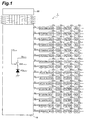
- Fig. 1 is an overall diagram of a photodetector 1 in accordance with an embodiment.
- Fig. 2 is a partial diagram of the photodetector 1 in accordance with the embodiment.
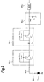
- FIG 3 is a circuit diagram of photodetector 1 of the embodiment.
- Fig. 4 is a timing chart for explaining operations of the photodetector 1 in accordance with the embodiment.
- FIG. 5 is a diagram of another circuit example of photodetector 1 of the embodiment.
- FIG 1 is an overall diagram of a photodetector 1 of the embodiment.
- FIG. 2 is a partial diagram of photodetector 1 of the embodiment. The details of a photodetection unit 10, shown in FIG 1 are shown in FIG 2.
- a photodetector 1 which is illustrated in these figures, is equipped with photodetection unit 10, (M ⁇ N) integrating circuits 20 1,1 to 20 M,N , (M ⁇ N) CDS circuits 30 1,1 to 30 M,N , (M ⁇ N) filter circuits 40 1,1 to 40 M,N , (M ⁇ N) A/D converters 50 1,1 to 50 M,N , and a control circuit 60.
- Photodetection unit 10 has (K ⁇ M ⁇ N) photodiodes PD 1,1,1 to PD K,M,N and (K ⁇ M ⁇ N) switches SW 1,1,1 to SW K,M,N .
- K indicates an integer no less than 2
- M indicates an integer no less than 1
- N indicates an integer no less than 2.
- k indicates integers no less than 1 and no more than K
- m indicates integers no less than 1 and no more than M
- n indicates integers no less than 1 and no more than N.
- K is set to 2 and M and N are both set to 4.
- Each photodiode PD k,m,n generates electric charges of an amount that is in accordance with an incident light intensity and accumulates these electric charges in a junction capacitance portion.
- Each photodiode PD k,m,n is positioned at the position of the m-th row and the (n + (k - 1)N)-th column.
- Switches SW k,m,n are provided in a one-to-one correspondence with respect to photodiodes PD k,m,n and are arranged between PD k,m,n and signal lines SL m,n .
- Each signal line SL m,n is connected to an input end of an integrating circuit 20 m,n .
- Each CDS (correlated double sampling) circuit 30 m,n inputs the voltage output from the corresponding integrating circuit 20 m,n and outputs a voltage expressing the fluctuation over a fixed time of this voltage.
- Each filter circuit 40 m,n inputs the voltage output from the corresponding CDS circuit 30 m,n , reduces the thermal noise component contained in this voltage, and outputs the voltage after reduction of the thermal noise component.
- Each filter circuit 40 m,n is preferably a low-pass filter with filter characteristics that can reduce thermal noise components.
- Each A/D converter 50 m,n inputs the voltage output from the corresponding filter circuit 40 m,n , performs A/D conversion of this voltage, and outputs a digital value that is in accordance with this voltage (analog value).
- Control circuit 60 outputs control signals for controlling the opening/closing of the respective (K ⁇ M ⁇ N) switches SW 1,1,1 to SW K,M,N, to control lines CL k,n .
- Control circuit 60 also controls the respective operations of integrating circuits 20 m,n, CDS circuits 30 m,n and A/D converters 50 m,n .
- FIG 3 is a circuit diagram of photodetector 1 of the present embodiment.
- photodiodes PD k,m,n switches SW k,m,n , integrating circuits 20 m,n, CDS circuits 30 m,n , filter circuits 40 m,n , and A/D converters 50 m,n are shown in the figure.
- Integrating circuit 20 m,n has an amplifier A 20 , an integrating capacitance element C 20 , and a switch SW 20 .
- the input terminal of amplifier A 20 is connected to signal line SL m,n .
- Integrating capacitance element C 20 and switch SW 20 are arranged in parallel between the input and output terminals of amplifier A 20 .
- the opening/closing of switch SW 20 is controlled by control unit 60. When switch SW 20 is closed, integrating capacitance element C 20 is discharged and the voltage output from integrating circuit 20 m,n is initialized.
- CDS circuit 30 m,n has an amplifier A 30 , an integrating capacitance element C 31 , a junction capacitance element C 32 , and a switch SW 30 .
- the input terminal of amplifier A 30 is connected via junction capacitance element C 32 to the output terminal of amplifier A 20 of integrating circuit 20 m,n .
- Integrating capacitance element C 31 and switch SW 30 are arranged in parallel between the input and output terminals of amplifier A 30 .
- the opening/closing of switch SW 30 is controlled by control unit 60. When switch SW 30 is closed, integrating capacitance element C 31 is discharged and the voltage output from CDS circuit 30 m,n is initialized.
- Filter circuit 40 m,n has a resistance element R 40 and a capacitance element C 40 .
- Resistance element R 40 is arranged between the input end and the output end of filter circuit 40 m,n and the output end thereof is connected via capacitance element C 40 to the ground potential.
- This filter circuit 40 m,n acts as a low-pass filter and in term of filter characteristics, the cutoff frequency thereof is in accordance with the resistance value of resistance element R 40 and the capacitance value of capacitance element C 40 .
- the characteristic values of the respective elements in the circuit diagram shown in FIG. 3 are, for example, as follows. That is, the sum of the junction capacitance value C d of photodiode PD k,m,,n and the parasitic capacitance value of signal line SL m,n is 220pF and the resistance value of signal line SL m,n is 1k ⁇ .
- the capacitance value C f of integrating capacitance element C 20 of integrating circuit 20 m,n is 1.25pF
- the frequency bandwidth B of amplifier A 20 of integrating circuit 20 m,n is 1MHz
- the input transistor's transconductance G m of amplifier A 20 is 10mS.
- the temperature T is 27°C.
- the thermal noise V n generated at amplifier A 20 of integrating circuit 20 m,n is 1210 ⁇ V mns . If the capacitance value of capacitance element C 40 of filter circuit 40 m,n is 100pF and the resistance value of resistance element R 40 of filter circuit 40 m,n is 20k ⁇ , the cutoff frequency of the filter characteristics of filter circuit 40 m,n will be 0.08MHz and the thermal noise component contained in the voltage output from filter circuit 40 m,n will be reduced to 724 ⁇ V mns .
- FIG 4 is a timing chart illustrating the operations of photodetector 1 of the present embodiment. With this photodetector 1, the first row to the M-th row operate in parallel.
- the opening/closing of switch SW 1,m,1 , the opening/closing of switch SW 1,m,2 , the opening/closing of switch SW 1,m,3 , the opening/closing of switch SW 1,m,4 , the opening/closing of switch SW 2,m,1 , the opening/closing of switch SW 2 , m,2 , the opening/closing of switch SW 2,m,3 , and the opening/closing of switch SW 2,m,4 are shown in that order from the top.
- the operations of photodetector 1 are divided into the eight periods of T 1,1 , T 1,2 , T 1,3 , T 1,4 , T 2,1 , T 2,2 , T 2,3 , and T 2,4 that cycle.
- the duration T of each of these periods T k,n is fixed.
- Switch SW 1,m,1 is closed during period T 1,1
- switch SW 1,m,2 is closed during period T 1,2
- switch SW 1,m,3 is closed during period T 1,3
- switch SW 1,m,4 is closed during period T 1,4
- switch SW 2,m,1 is closed during period T 2,1
- switch SW 2,m,2 is closed during period T 2,2
- switch SW 2,m,3 is closed during period T 2,3
- switch SW 2,m,4 is closed during period T 2,4 . Subsequently, such opening and closing of the switches are repeated.
- Switch SW 1,m,1 is closed during period T 1,1 . Also, prior to this period T 1,1 , switch SW 20 of integrating circuit 20 m,1 closes once and then opens and the output voltage of integrating circuit 20 m,1 is thereby initialized.
- switch SW 1,m,1 closes, the electric charges generated in photodiode PD 1,m,1 and accumulated in the junction capacitance portion until then are input via switch SW 1,m,1 and signal line SL m,1 into integrating circuit 20 m,1 and become accumulated in integrating capacitance element C 20 of integrating circuit 20 m,1 and a voltage that is in accordance with the amount of the accumulated electric charges is output from integrating circuit 20 m,1 .
- the output voltage of integrating circuit 20 m,1 is input into CDS circuit 30 m,l . From this CDS circuit 30 m,1 is output a voltage that is in accordance with the amount of fluctuation of the output voltage of integrating circuit 20 m,1 in the fixed duration from period T 1,1 to T 1,2 .
- the output voltage of CDS circuit 30 m,1 is input into filter circuit 40 m,1 and the thermal noise component is reduced. However, due to the filter characteristics of filter circuit 40 m,1 , the output voltage waveform of filter circuit 40 m,1 is dulled in comparison to the output voltage waveform of CDS circuit 30 m,1 .
- this voltage is A/D converted by A/D converter 50 m,1 and a digital value is output from A/D converter 50 m,1 in period T 1,3 .
- the digital value that is output from A/D converter 50 m,1 in period T 1,3 is in accordance with the amount of electric charges that have moved from the junction capacitance portion of photodiode PD 1,m,1 to integrating capacitance element C 20 of integrating circuit 20 m,1 and thus in accordance with the intensity of light incident on photodiode PD 1,m,1 in period T 1,1 .
- Switch SW 2,m,1 is closed during period T 2,1 .
- switch SW 20 of integrating circuit 20 m,1 closes once and then opens and the output voltage of integrating circuit 20 m,1 is thereby initialized.
- switch SW 2,m,1 closes, the electric charges generated in photodiode PD 2,m,1 and accumulated in the junction capacitance portion until then are input via switch SW 2,m,1 and signal line SL m,1 into integrating circuit 20 m,1 and are accumulated in integrating capacitance element C 20 of integrating circuit 20 m,1 and a voltage that is in accordance with the amount of the accumulated electric charges is output from integrating circuit 20 m,1 .
- the output voltage of integrating circuit 20 m,1 is input into CDS circuit 30 m,1 . From this CDS circuit 30 m,1 is output a voltage that is in accordance with the amount of fluctuation of the output voltage of integrating circuit 20 m,1 in the fixed duration from period T 2,1 to T 2,2 .
- the output voltage of CDS circuit 30 m,1 is input into filter circuit 40 m,1 and the thermal noise component is reduced. However, due to the filter characteristics of filter circuit 40 m,1 , the output voltage waveform of filter circuit 40 m,1 is dulled in comparison to the output voltage waveform of CDS circuit 30 m,1 .
- this voltage is A/D converted by A/D converter 50 m,1 and a digital value is output from A/D converter 50 m,1 in period T 2,3 .
- the digital value that is output from A/D converter 50 m,1 in period T 2,3 is in accordance with the amount of electric charges that have moved from the junction capacitance portion of photodiode PD 2,m,1 to integrating capacitance element C 20 of integrating circuit 20 m,1 and thus in accordance with the intensity of light incident on photodiode PD 2,m,1 in period T 2,1 .
- switch SW 1,m,1 switch SW 2,m,1 , integrating circuit 20 m,1, CDS circuit 30 m,1, filter circuit 40 m,1, and A/D converter 50 m,1, that is, the operations in the case where n is 1 was described.
- a digital value that is in accordance with the intensity of light incident on photodiode PD 1,m,1 is thus output in period T 1,3
- a digital value that is in accordance with the intensity of light incident on photodiode PD 1,m,2 is output in period T 1,4
- a digital value that is in accordance with the intensity of light incident on photodiode PD 1,m,3 is output in period T 2,1
- a digital value that is in accordance with the intensity of light incident on photodiode PD 1,m,4 is output in period T 2,2
- a digital value that is in accordance with the intensity of light incident on photodiode PD 2,m,1 is output in period T 2,3
- a digital value that is in accordance with the intensity of light incident on photodiode PD 2,m,2 is output in period T 2,4
- a digital value that is in accordance with the intensity of light incident on photodiode PD 2,m,3 is output in the subsequent period T 1,1
- each of the electric charge accumulation operation in integrating circuit 20 m,n, the CDS operation in CDS circuit 30 m,n, the filtering operation in filter circuit 40 m,n, and the A/D conversion operation in A/D converter 50 m,n is carried out at each time (N ⁇ T).
- the thermal noise component contained in the voltage output from integrating circuit 20 m,n is reduced by filter circuit 40 m,n . Also, though the voltage waveform output from filter circuit 40 m,n is dulled, the operations from the electric charge accumulation in integrating circuit 20 m,n to the A/D conversion in A/D converter 50 m,n are carried out at each time (N ⁇ T), and the voltage that is output from filter circuit 40 m,n is A/D converted by A/D converter 50 m,n at the point at which it has stabilized.
- the S/N ratio of photodetection can be improved while maintaining high speed of photodetection.
- CDS circuit 30 m,n since by the provision of CDS circuit 30 m,n, the offset fluctuation of amplifier A 20 of integrating circuit 20 m,n, is eliminated by CDS circuit 30 m,n, the S/N ratio of photodetection is improved from this point as well.
- CDS circuit 30 m,n also contains amplifier A 30 , the thermal noise generated at this amplifier A 30 is minute in comparison to the thermal noise generated at amplifier A 20 included in integrating circuit 20 m,n .
- the photodetection data obtained by photodetector 1 are output as digital values, storage and image processing of the photodetection data can be carried out readily. Also, since the requirement of high-speed processing is relaxed in terms of A/D converter 50 m,n , the increase of consumption power at A/D converter 50 m,n is also restrained.
- each photodiode PD k,m,n is positioned at the position of the m-th row and the (n + (k - 1)N)-th column, and the processes (electric charge accumulation, CDS, filtering, and A/D conversion) regarding photodiodes PD k,m,n are carried out in the order of alignment in each column for each row, the storage and image processing of the photodetection data obtained by the photodetector 1 are facilitated from this point as well.
- filter circuit 40 m,n was arranged at a stage subsequent CDS circuit 30 m,n
- the filter circuit may instead be arranged between integrating circuit 20 m,n and CDS circuit 30 m,n .
- the filter circuit that is arranged between integrating circuit 20 m,n and CDS circuit 30 m,n may have the same arrangement as filter circuit 40 m,n described above, it may instead be arranged from just a resistance element R as shown in FIG 5. This resistance element R can also act as a low-pass filter.
- the thermal component that is contained in the voltage output from each integrating circuit is reduced by a filter circuit, and the voltage after reduction of the thermal noise component is output from the filter circuit. Both a good S/N ratio and a high speed can thus be secured with this photodetector.
Landscapes
- Engineering & Computer Science (AREA)
- Multimedia (AREA)
- Signal Processing (AREA)
- Photometry And Measurement Of Optical Pulse Characteristics (AREA)
- Transforming Light Signals Into Electric Signals (AREA)
- Solid State Image Pick-Up Elements (AREA)
Abstract
Description
Claims (4)
- A photodetector comprising:(K × M × N) photodiodes PDk,m,n (K being an integer of no less than 2; k being integers of no less than 1 and no more than K; M being an integer of no less than 1; m being integers of no less than 1 and no more than M; N being an integer of no less than 2; and n being integers of no less than 1 and no more than N), each generating an electric charge by an amount corresponding to an intensity of light incident thereon;(M × N) integrating circuits, one of each being provided in correspondence to K photodiodes PDk,m,n (k = 1 to K) among the (K × M × N) photodiodes PDk,m,n and each successively inputting and accumulating the electric charges generated at the K photodiodes PDk,m,n (k = 1 to K) and outputting a voltage that is in accordance with the amount of the accumulated electric charges; and(M × N) filter circuits, one of each being provided in correspondence to each of the (M × N) integrating circuits and each reducing the thermal noise component contained in the voltage output from the corresponding integrating circuit and outputting the voltage after reduction of the thermal noise component.
- The photodetector according to Claim 1, further comprising CDS circuits, each being arranged between said integrating circuit and said filter circuit, inputting the voltage output from the integrating circuit, and outputting a voltage expressing the fluctuation of the input voltage over a fixed time.
- The photodetector according to Claim 1, further comprising A/D converters, each inputting the voltage output from said filter circuit, performing A/D conversion on this voltage, and outputting a digital value that is in accordance with this voltage.
- The photodetector according to Claim 1 , wherein the (K × M × N) photodiodes PDk,m,n are arranged in M rows and (K × N) columns either two-dimensionally (when M = 2) or one-dimensionally (when M = 1), with each photodiode PDk,m,n being positioned at the position of the m-th row and (n + (k - 1)N)-th column.
Applications Claiming Priority (3)
| Application Number | Priority Date | Filing Date | Title |
|---|---|---|---|
| JP2002364123 | 2002-12-16 | ||
| JP2002364123A JP4293588B2 (en) | 2002-12-16 | 2002-12-16 | Photodetector |
| PCT/JP2003/016114 WO2004056093A1 (en) | 2002-12-16 | 2003-12-16 | Optical sensor |
Publications (3)
| Publication Number | Publication Date |
|---|---|
| EP1575281A1 true EP1575281A1 (en) | 2005-09-14 |
| EP1575281A4 EP1575281A4 (en) | 2009-08-19 |
| EP1575281B1 EP1575281B1 (en) | 2018-11-28 |
Family
ID=32588225
Family Applications (1)
| Application Number | Title | Priority Date | Filing Date |
|---|---|---|---|
| EP03780794.8A Expired - Lifetime EP1575281B1 (en) | 2002-12-16 | 2003-12-16 | Optical sensor |
Country Status (6)
| Country | Link |
|---|---|
| US (1) | US7612815B2 (en) |
| EP (1) | EP1575281B1 (en) |
| JP (1) | JP4293588B2 (en) |
| CN (1) | CN100461836C (en) |
| AU (1) | AU2003289366A1 (en) |
| WO (1) | WO2004056093A1 (en) |
Families Citing this family (5)
| Publication number | Priority date | Publication date | Assignee | Title |
|---|---|---|---|---|
| JP2004200794A (en) * | 2002-12-16 | 2004-07-15 | Hamamatsu Photonics Kk | Optical detector |
| JP5407798B2 (en) * | 2009-11-20 | 2014-02-05 | リコーイメージング株式会社 | Focus detection apparatus and image signal processing apparatus |
| KR101077408B1 (en) * | 2010-02-05 | 2011-10-26 | 서강대학교산학협력단 | CMOS Image Sensor |
| JP5620693B2 (en) * | 2010-02-26 | 2014-11-05 | パナソニック株式会社 | Solid-state imaging device, driving method thereof, and camera |
| JP5858652B2 (en) * | 2011-06-08 | 2016-02-10 | キヤノン株式会社 | Solid-state imaging device and driving method of solid-state imaging device |
Family Cites Families (26)
| Publication number | Priority date | Publication date | Assignee | Title |
|---|---|---|---|---|
| US4902886A (en) * | 1989-01-23 | 1990-02-20 | Hewlett-Packard Company | Noise reduction for photodiode arrays |
| JPH08331459A (en) * | 1995-06-02 | 1996-12-13 | Hamamatsu Photonics Kk | Solid-state imaging device |
| JP3308146B2 (en) * | 1995-06-02 | 2002-07-29 | 浜松ホトニクス株式会社 | Solid-state imaging device |
| JPH09238286A (en) * | 1996-02-29 | 1997-09-09 | Toshiba Corp | Digital optical sensor |
| JP4035194B2 (en) | 1996-03-13 | 2008-01-16 | キヤノン株式会社 | X-ray detection apparatus and X-ray detection system |
| JP3798462B2 (en) * | 1996-04-01 | 2006-07-19 | 浜松ホトニクス株式会社 | Solid-state imaging device |
| JP3817294B2 (en) * | 1996-04-01 | 2006-09-06 | 浜松ホトニクス株式会社 | Solid-state imaging device |
| US5892540A (en) * | 1996-06-13 | 1999-04-06 | Rockwell International Corporation | Low noise amplifier for passive pixel CMOS imager |
| US6031570A (en) * | 1997-03-19 | 2000-02-29 | Omnivision Technologies, Inc. | Image acquisition and processing system |
| US6344877B1 (en) * | 1997-06-12 | 2002-02-05 | International Business Machines Corporation | Image sensor with dummy pixel or dummy pixel array |
| JP4098884B2 (en) * | 1998-07-08 | 2008-06-11 | 浜松ホトニクス株式会社 | Solid-state imaging device |
| JP4398095B2 (en) * | 1998-09-09 | 2010-01-13 | 浜松ホトニクス株式会社 | Solid-state imaging device |
| EP1158789B1 (en) * | 1999-01-29 | 2006-09-27 | Hamamatsu Photonics K.K. | Photodetector device |
| JP4358351B2 (en) * | 1999-04-27 | 2009-11-04 | 浜松ホトニクス株式会社 | Photodetector |
| JP2000324397A (en) * | 1999-05-12 | 2000-11-24 | Sony Corp | Solid-state imaging device |
| JP4119052B2 (en) * | 1999-07-16 | 2008-07-16 | 浜松ホトニクス株式会社 | Photodetector |
| EP1206131B1 (en) * | 1999-08-05 | 2005-12-07 | Hamamatsu Photonics K.K. | Solid-state imaging device and range finding device |
| JP4424796B2 (en) * | 1999-11-18 | 2010-03-03 | 浜松ホトニクス株式会社 | Photodetector |
| US6873364B1 (en) * | 2000-06-08 | 2005-03-29 | Micron Technology, Inc. | Low-power signal chain for image sensors |
| JP4489914B2 (en) * | 2000-07-27 | 2010-06-23 | 浜松ホトニクス株式会社 | A / D converter and solid-state imaging device |
| JP2002051264A (en) * | 2000-08-03 | 2002-02-15 | Sharp Corp | Correlated double sampling circuit |
| US7286172B2 (en) * | 2000-08-03 | 2007-10-23 | Hamamatsu Photonics K.K. | Optical sensor |
| GB0020280D0 (en) * | 2000-08-18 | 2000-10-04 | Vlsi Vision Ltd | Modification of column fixed pattern column noise in solid image sensors |
| JP2002199282A (en) | 2000-12-26 | 2002-07-12 | Sharp Corp | Photoelectric conversion device and driving method thereof |
| JP4414646B2 (en) * | 2002-11-18 | 2010-02-10 | 浜松ホトニクス株式会社 | Photodetector |
| JP2004200794A (en) * | 2002-12-16 | 2004-07-15 | Hamamatsu Photonics Kk | Optical detector |
-
2002
- 2002-12-16 JP JP2002364123A patent/JP4293588B2/en not_active Expired - Lifetime
-
2003
- 2003-12-16 CN CNB2003801061695A patent/CN100461836C/en not_active Expired - Fee Related
- 2003-12-16 WO PCT/JP2003/016114 patent/WO2004056093A1/en not_active Ceased
- 2003-12-16 AU AU2003289366A patent/AU2003289366A1/en not_active Abandoned
- 2003-12-16 US US10/539,068 patent/US7612815B2/en not_active Expired - Fee Related
- 2003-12-16 EP EP03780794.8A patent/EP1575281B1/en not_active Expired - Lifetime
Also Published As
| Publication number | Publication date |
|---|---|
| JP2004200792A (en) | 2004-07-15 |
| US7612815B2 (en) | 2009-11-03 |
| JP4293588B2 (en) | 2009-07-08 |
| EP1575281A4 (en) | 2009-08-19 |
| EP1575281B1 (en) | 2018-11-28 |
| WO2004056093A1 (en) | 2004-07-01 |
| CN100461836C (en) | 2009-02-11 |
| US20060227229A1 (en) | 2006-10-12 |
| CN1726698A (en) | 2006-01-25 |
| AU2003289366A1 (en) | 2004-07-09 |
Similar Documents
| Publication | Publication Date | Title |
|---|---|---|
| US8017901B2 (en) | Photodetector | |
| Decker et al. | A 256/spl times/256 CMOS imaging array with wide dynamic range pixels and column-parallel digital output | |
| US9787923B2 (en) | Correlated double sampled (CDS) pixel sense amplifier | |
| EP2063535A1 (en) | Ad converter circuit and optical sensor | |
| EP2517461B1 (en) | Column output circuits for image sensors | |
| JP2000032342A (en) | Solid-state imaging device | |
| EP1757912B1 (en) | Photo detector apparatus | |
| US7989753B2 (en) | Photodetector having wide dynamic range and low temperature dependence | |
| US8564704B2 (en) | Solid-state imaging device having transimpedance amplifier | |
| EP3871407B1 (en) | Ultra-high dynamic range cmos sensor | |
| JP2009141401A (en) | Solid-state imaging device | |
| US7612815B2 (en) | Optical sensor | |
| EP1136798B1 (en) | Photodetector device | |
| KR101332536B1 (en) | Solid - state imaging apparatus | |
| US20030132871A1 (en) | Method for converting an analog signal into a digital signal and electromagnetic radiation sensor using same | |
| EP1575282B1 (en) | Optical sensor | |
| US20050162530A1 (en) | Correlated double sampling circuit, signal processing circuit, and solid-state imaging apparatus | |
| EP3646582B1 (en) | Ultra-low noise amplifier adapted for cmos imaging sensors | |
| EP1758376B1 (en) | Sensor apparatus | |
| JP2006203308A (en) | Imaging device | |
| JPH05207378A (en) | Method for driving ccd solid-state image pickup device | |
| JP2007096485A (en) | Solid-state imaging device | |
| WO2004110058A1 (en) | Solid state imaging device |
Legal Events
| Date | Code | Title | Description |
|---|---|---|---|
| PUAI | Public reference made under article 153(3) epc to a published international application that has entered the european phase |
Free format text: ORIGINAL CODE: 0009012 |
|
| 17P | Request for examination filed |
Effective date: 20050616 |
|
| AK | Designated contracting states |
Kind code of ref document: A1 Designated state(s): AT BE BG CH CY CZ DE DK EE ES FI FR GB GR HU IE IT LI LU MC NL PT RO SE SI SK TR |
|
| AX | Request for extension of the european patent |
Extension state: AL LT LV MK |
|
| DAX | Request for extension of the european patent (deleted) | ||
| RBV | Designated contracting states (corrected) |
Designated state(s): DE FR GB NL |
|
| A4 | Supplementary search report drawn up and despatched |
Effective date: 20090721 |
|
| 17Q | First examination report despatched |
Effective date: 20091030 |
|
| GRAP | Despatch of communication of intention to grant a patent |
Free format text: ORIGINAL CODE: EPIDOSNIGR1 |
|
| INTG | Intention to grant announced |
Effective date: 20180302 |
|
| GRAJ | Information related to disapproval of communication of intention to grant by the applicant or resumption of examination proceedings by the epo deleted |
Free format text: ORIGINAL CODE: EPIDOSDIGR1 |
|
| GRAJ | Information related to disapproval of communication of intention to grant by the applicant or resumption of examination proceedings by the epo deleted |
Free format text: ORIGINAL CODE: EPIDOSDIGR1 |
|
| GRAP | Despatch of communication of intention to grant a patent |
Free format text: ORIGINAL CODE: EPIDOSNIGR1 |
|
| INTC | Intention to grant announced (deleted) | ||
| INTG | Intention to grant announced |
Effective date: 20180720 |
|
| GRAS | Grant fee paid |
Free format text: ORIGINAL CODE: EPIDOSNIGR3 |
|
| GRAA | (expected) grant |
Free format text: ORIGINAL CODE: 0009210 |
|
| AK | Designated contracting states |
Kind code of ref document: B1 Designated state(s): DE FR GB NL |
|
| REG | Reference to a national code |
Ref country code: GB Ref legal event code: FG4D |
|
| REG | Reference to a national code |
Ref country code: DE Ref legal event code: R096 Ref document number: 60351668 Country of ref document: DE |
|
| PGFP | Annual fee paid to national office [announced via postgrant information from national office to epo] |
Ref country code: NL Payment date: 20181205 Year of fee payment: 16 Ref country code: DE Payment date: 20181204 Year of fee payment: 16 |
|
| REG | Reference to a national code |
Ref country code: NL Ref legal event code: FP |
|
| PGFP | Annual fee paid to national office [announced via postgrant information from national office to epo] |
Ref country code: FR Payment date: 20181127 Year of fee payment: 16 Ref country code: GB Payment date: 20181212 Year of fee payment: 16 |
|
| REG | Reference to a national code |
Ref country code: DE Ref legal event code: R097 Ref document number: 60351668 Country of ref document: DE |
|
| PLBE | No opposition filed within time limit |
Free format text: ORIGINAL CODE: 0009261 |
|
| STAA | Information on the status of an ep patent application or granted ep patent |
Free format text: STATUS: NO OPPOSITION FILED WITHIN TIME LIMIT |
|
| 26N | No opposition filed |
Effective date: 20190829 |
|
| REG | Reference to a national code |
Ref country code: DE Ref legal event code: R119 Ref document number: 60351668 Country of ref document: DE |
|
| REG | Reference to a national code |
Ref country code: NL Ref legal event code: MM Effective date: 20200101 |
|
| GBPC | Gb: european patent ceased through non-payment of renewal fee |
Effective date: 20191216 |
|
| PG25 | Lapsed in a contracting state [announced via postgrant information from national office to epo] |
Ref country code: NL Free format text: LAPSE BECAUSE OF NON-PAYMENT OF DUE FEES Effective date: 20200101 |
|
| PG25 | Lapsed in a contracting state [announced via postgrant information from national office to epo] |
Ref country code: FR Free format text: LAPSE BECAUSE OF NON-PAYMENT OF DUE FEES Effective date: 20191231 Ref country code: DE Free format text: LAPSE BECAUSE OF NON-PAYMENT OF DUE FEES Effective date: 20200701 Ref country code: GB Free format text: LAPSE BECAUSE OF NON-PAYMENT OF DUE FEES Effective date: 20191216 |