EP1575083A2 - Method of manufacturing a semiconductor device and semiconductor device obtainable with such a method - Google Patents
Method of manufacturing a semiconductor device and semiconductor device obtainable with such a method Download PDFInfo
- Publication number
- EP1575083A2 EP1575083A2 EP05003848A EP05003848A EP1575083A2 EP 1575083 A2 EP1575083 A2 EP 1575083A2 EP 05003848 A EP05003848 A EP 05003848A EP 05003848 A EP05003848 A EP 05003848A EP 1575083 A2 EP1575083 A2 EP 1575083A2
- Authority
- EP
- European Patent Office
- Prior art keywords
- region
- gate
- semiconductor body
- channel region
- trench
- Prior art date
- Legal status (The legal status is an assumption and is not a legal conclusion. Google has not performed a legal analysis and makes no representation as to the accuracy of the status listed.)
- Withdrawn
Links
Images

Classifications
-
- H—ELECTRICITY
- H10—SEMICONDUCTOR DEVICES; ELECTRIC SOLID-STATE DEVICES NOT OTHERWISE PROVIDED FOR
- H10D—INORGANIC ELECTRIC SEMICONDUCTOR DEVICES
- H10D30/00—Field-effect transistors [FET]
- H10D30/01—Manufacture or treatment
- H10D30/021—Manufacture or treatment of FETs having insulated gates [IGFET]
- H10D30/023—Manufacture or treatment of FETs having insulated gates [IGFET] having multiple independently-addressable gate electrodes influencing the same channel
-
- H—ELECTRICITY
- H10—SEMICONDUCTOR DEVICES; ELECTRIC SOLID-STATE DEVICES NOT OTHERWISE PROVIDED FOR
- H10D—INORGANIC ELECTRIC SEMICONDUCTOR DEVICES
- H10D30/00—Field-effect transistors [FET]
- H10D30/60—Insulated-gate field-effect transistors [IGFET]
- H10D30/611—Insulated-gate field-effect transistors [IGFET] having multiple independently-addressable gate electrodes influencing the same channel
-
- H—ELECTRICITY
- H10—SEMICONDUCTOR DEVICES; ELECTRIC SOLID-STATE DEVICES NOT OTHERWISE PROVIDED FOR
- H10D—INORGANIC ELECTRIC SEMICONDUCTOR DEVICES
- H10D84/00—Integrated devices formed in or on semiconductor substrates that comprise only semiconducting layers, e.g. on Si wafers or on GaAs-on-Si wafers
- H10D84/01—Manufacture or treatment
- H10D84/0123—Integrating together multiple components covered by H10D12/00 or H10D30/00, e.g. integrating multiple IGBTs
- H10D84/0126—Integrating together multiple components covered by H10D12/00 or H10D30/00, e.g. integrating multiple IGBTs the components including insulated gates, e.g. IGFETs
- H10D84/0165—Integrating together multiple components covered by H10D12/00 or H10D30/00, e.g. integrating multiple IGBTs the components including insulated gates, e.g. IGFETs the components including complementary IGFETs, e.g. CMOS devices
- H10D84/0167—Manufacturing their channels
-
- H—ELECTRICITY
- H10—SEMICONDUCTOR DEVICES; ELECTRIC SOLID-STATE DEVICES NOT OTHERWISE PROVIDED FOR
- H10D—INORGANIC ELECTRIC SEMICONDUCTOR DEVICES
- H10D84/00—Integrated devices formed in or on semiconductor substrates that comprise only semiconducting layers, e.g. on Si wafers or on GaAs-on-Si wafers
- H10D84/01—Manufacture or treatment
- H10D84/0123—Integrating together multiple components covered by H10D12/00 or H10D30/00, e.g. integrating multiple IGBTs
- H10D84/0126—Integrating together multiple components covered by H10D12/00 or H10D30/00, e.g. integrating multiple IGBTs the components including insulated gates, e.g. IGFETs
- H10D84/0165—Integrating together multiple components covered by H10D12/00 or H10D30/00, e.g. integrating multiple IGBTs the components including insulated gates, e.g. IGFETs the components including complementary IGFETs, e.g. CMOS devices
- H10D84/017—Manufacturing their source or drain regions, e.g. silicided source or drain regions
-
- H—ELECTRICITY
- H10—SEMICONDUCTOR DEVICES; ELECTRIC SOLID-STATE DEVICES NOT OTHERWISE PROVIDED FOR
- H10D—INORGANIC ELECTRIC SEMICONDUCTOR DEVICES
- H10D84/00—Integrated devices formed in or on semiconductor substrates that comprise only semiconducting layers, e.g. on Si wafers or on GaAs-on-Si wafers
- H10D84/01—Manufacture or treatment
- H10D84/0123—Integrating together multiple components covered by H10D12/00 or H10D30/00, e.g. integrating multiple IGBTs
- H10D84/0126—Integrating together multiple components covered by H10D12/00 or H10D30/00, e.g. integrating multiple IGBTs the components including insulated gates, e.g. IGFETs
- H10D84/0165—Integrating together multiple components covered by H10D12/00 or H10D30/00, e.g. integrating multiple IGBTs the components including insulated gates, e.g. IGFETs the components including complementary IGFETs, e.g. CMOS devices
- H10D84/0172—Manufacturing their gate conductors
-
- H—ELECTRICITY
- H10—SEMICONDUCTOR DEVICES; ELECTRIC SOLID-STATE DEVICES NOT OTHERWISE PROVIDED FOR
- H10D—INORGANIC ELECTRIC SEMICONDUCTOR DEVICES
- H10D84/00—Integrated devices formed in or on semiconductor substrates that comprise only semiconducting layers, e.g. on Si wafers or on GaAs-on-Si wafers
- H10D84/01—Manufacture or treatment
- H10D84/02—Manufacture or treatment characterised by using material-based technologies
- H10D84/03—Manufacture or treatment characterised by using material-based technologies using Group IV technology, e.g. silicon technology or silicon-carbide [SiC] technology
- H10D84/038—Manufacture or treatment characterised by using material-based technologies using Group IV technology, e.g. silicon technology or silicon-carbide [SiC] technology using silicon technology, e.g. SiGe
Definitions
- the invention relates to a method of manufacturing a semiconductor device comprising a dual gate field effect transistor, in which method a semiconductor body with a surface and of silicon is provided with a source region and a drain region of a first conductivity type and with a channel region of a second conductivity type, opposite to the first conductivity type, between the source region and the drain region and with a first gate region separated from the channel region by a first gate dielectric and situated on one side of the channel region and with a second gate region separated from the channel region by a second gate dielectric and situated on an opposite side of the channel region and wherein both gate regions are formed within a trench formed in the semiconductor body.
- the use of a double gate structure can generally be used to reduce leakage current when the transistor is off and increases drive current when the transistor is on. These aspects become increasingly important as demands on further miniaturization, lower power use and better high-frequency behavior in CMOS devices are still relevant.
- the invention relates to a semiconductor device of the above construction.
- a method as mentioned in the opening paragraph is known from US patent US 6,580,137 B2 that has been issued on June 17, 2003. Therein (see e.g. figure 12B and the description columns 7 to 14 ) a method is described in a dual gate transistor is provided in a trench. One of the gate regions is formed at the bottom part of the trench while the other gate region is formed in the upper part of the trench, the channel region being interposed between the two gate regions.
- a drawback of the known method is that it is rather complicated and requires relatively many steps. Thus, there is still the need for a method for forming a dual gate transistor which can be easily incorporated in present and future CMOS technology.
- a method of the type described in the opening paragraph is characterized in that the first gate region is formed within a first trench and the second gate region is formed within a second trench, the channel region is formed by the part of the semiconductor body between the first and second trench and the source and drain regions are formed at the surface of the semiconductor body.
- Such a method is relatively simple and is very well compatible with present and most likely with future CMOS technology.
- the dual gate transistor formed is on the one hand vertical since the channel in the channel region is formed in a plane perpendicular to the surface of the semiconductor body and on the other hand horizontal since the source and drain regions are formed at the surface of the semiconductor body in a conventional manner.
- the dual gates that are present in two adjacent trenches offer a more efficient control over the channel.
- two parallel trenches are formed in the surface of the semiconductor body of which the walls are provided with a dielectric layer and which are filled with a conductive material by depositing a conductive layer on the semiconductor body of which the parts on top of the surface of the semiconductor body are removed by chemical mechanical polishing.
- the conductive material is preferable a metal.
- the conductive material can be formed in two stages. E.g. by depositing a silicon layer and by depositing a metal layer, for example a nickel layer, on top of the silicon layer followed by a low temperature anneal, e.g. a few minutes at 300 degrees Celsius, in which a nickel silicide is formed offering a high conduction.
- the source and drain regions are formed by depositing a strip-shaped mask layer on the surface of the semiconductor body which bridges the two regions were the trenches are formed or to be formed after which dopants of the first conductivity type are introduced into the semiconductor body on both sides of the strip-shaped mask layer.
- the source and drain regions are formed after the trenches are formed and filled with the conductive material / metal.
- Ion implantation is a very suitable technique to form source and drain regions in a method according to the invention.
- SPE Solid Phase Epitaxy
- two dual gate transistors are formed in the semiconductor body and next to each other by forming three trenches in the semiconductor body of which the middle one forms a common gate for both two dual gate transistors.
- an inverter is formed in a simple manner which is also very compact.
- one of the two dual gate transistors is formed as an npn transistor while the other one is formed as a pnp transistor.
- the latter is easily obtainable in a method according to the invention as both the source and drain regions are formed at the surface of the semiconductor body.
- the channel region of one of the two transistors may be provided with another - is opposite - conductivity type by a local implantation at the surface of the semiconductor body.
- the source and drain regions of the dual gate transistor(s) are separated from the semiconductor body on a side opposite to the channel region(s) by further trenches.
- the invention further relates to a semiconductor device comprising a dual gate field effect transistor, having a semiconductor body with a surface and of silicon and with a source region and a drain region of a first conductivity type and with a channel region of a second conductivity type, opposite to the first conductivity type, between the source region and the drain region and with a first gate region separated from the channel region by a first gate dielectric and situated on one side of the channel region and with a second gate region separated from the channel region by a second gate dielectric and situated on an opposite side of the channel region, and wherein both gate regions are formed within a trench formed in the semiconductor body.
- such a device is characterized in that the first gate region is formed within a first trench and the second gate region is formed within a second trench, the channel region is formed by the part of the semiconductor body between the first and second trench and the source and drain regions are formed at the surface of the semiconductor body.
- Such a device is very suitable for use in future CMOS ICs and may easily be obtained using a method according to the invention.
- a device comprises two neighboring dual gate transistors having one gate in common.
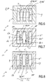
- Figures 1 through 8 are sectional (figures 1-5) or top (figures 6-8) views of a semiconductor device with a dual gate field effect transistor according to the invention at various stages in the manufacture of the device by means of a method in accordance with the invention.
- the method for forming the device 10 starts (see figure 1) in this example with a substrate 11 which in this case, but not necessarily, comprises silicon and thus also forms part of the semiconductor body 1 of silicon and which in this example is of the p-type conductivity.
- the substrate 11 also can have the opposite conductivity type.
- the region 11 may also be e.g. an n-well (or p-well for that matter) within a silicon substrate of the opposite conductivity type, e.g.
- the substrate / region 11 comprises the channel region 4 of the transistor to be formed in the form of an opposite conductivity type layer 12, here of the n-type.
- This layer may be formed by implantation, diffusion or epitaxy.
- transistors of both of the NMOS and PMOS type will be present.
- a mask 13 is deposited on the semiconductor body 1 which is formed by photolithography if desired after deposition of a dielectric material which then comprises a photoresist or a dielectric respectively.
- the mask 13 is used to form in this example three trenches 7A,7B,7C by means of anisotropic (plasma) etching.
- the regions 4,4' of the semiconductor body 1 between each pair of neighboring trenches 7 will form the channel regions of two dual gate transistors T1,T2 to be formed.
- the depth of the trenches 7 is such that the pn-junction between regions 11,12 is crossed.
- an dielectric layer 60 is deposited on the semiconductor body 1, e.g. comprising silicondioxide.
- a conducting layer 80 in this case a metal layer 80 which comprises in this example wolfram, is deposited on the semiconductor body 1.
- the thickness of layer 80 is chosen such that the trenches 7 are completely filled.
- the layer 80 may be formed by CVD or by physical techniques like evaporation or sputtering.
- the semiconductor body 1 is planarized by chemical-mechanical polishing such that the regions of the metal layer 80 outside the trenches 7 are removed.
- the remaining parts of this layer 80 form the material 8 of four gate regions (5A, 5B), (5A', 5B') of the two transistors T1, T2 to be formed, wherein the gate regions 5B and 5A' form a common gate region for both transistors.
- the mask 9 is strip-shaped, has a small width and bridges the two channel regions 4,4' of the two transistors to be formed.
- dopant of a conductivity type opposite to that of the channel regions 4,4' in this case p-type impurities like Boron, are introduced in the semiconductor body 1, here by means of ion implantation.
- source and drain regions 2,3,2',3' of the two transistors are formed.
- the mask 17 is removed again.
- an additional implantation is used to create the channel region of one of the two transistors. Also source and drain formation is done in separate steps during which one of the two transistors is masked
- a further trench 17 is formed around the two transistors T1,T2. This is done in a similar way as for the trenches 7.
- the further trench 17 may be partly or completely filled with an electrically insulating material, e.g. in the same way as described before for the trenches 7.
- n-MOSFET is completed by deposition of a pre-metal dielectric, e.g. of silicondioxide, followed by patterning thereof, deposition of a contact metal layer, e.g. of aluminum, again followed by patterning by which contact regions are formed.
- a pre-metal dielectric e.g. of silicondioxide
- a contact metal layer e.g. of aluminum
- a (self-aligned) silicide process may further be used to contact the source- and drain regions 2,3 and the gate region 5 in case the latter comprises e.g. polysilicon as the conducting material 8.
Landscapes
- Insulated Gate Type Field-Effect Transistor (AREA)
- Metal-Oxide And Bipolar Metal-Oxide Semiconductor Integrated Circuits (AREA)
Abstract
Description
Claims (11)
- Method of manufacturing a semiconductor device (10) comprising a dual gate field effect transistor, in which method a semiconductor body (1) with a surface and of silicon is provided with a source region (2) and a drain region (3) of a first conductivity type and with a channel region (4) of a second conductivity type, opposite to the first conductivity type, between the source region (2) and the drain region (3) and with a first gate region (5A) separated from the channel region (4) by a first gate dielectric (6A) and situated on one side of the channel region (4) and with a second gate region (5B) separated from the channel region (4) by a second gate dielectric (6B) and situated on an opposite side of the channel region (4), and wherein both gate regions (5A, 5B) are formed within a trench (7) formed in the semiconductor body, characterized in that the first gate region (5A) is formed within a first trench (7A) and the second gate region (5B) is formed within a second trench (7B), the channel region (4) is formed by the part of the semiconductor body (1) between the first and second trench (7A,7B) and the source and drain regions (2,3) are formed at the surface of the semiconductor body (1).
- Method as claimed in claim 1, characterized in that two parallel trenches (7A,7B) are formed in the surface of the semiconductor body of which the walls are provided with a dielectric layer (60) and which are filled with a conductive material (8) by depositing a conductive layer (80) on the semiconductor body (1) of which the parts on top of the surface of the semiconductor body (1) are removed by chemical mechanical polishing.
- Method as claimed in claim 2, characterized in that for the conductive layer (80) a metal layer is chosen.
- Method as claimed in any of the preceding claims, characterized in that a the source and drain regions (2,3) are formed by depositing a strip-shaped mask layer (9) on the surface of the semiconductor body (1) which bridges the two regions where the trenches (7A, 7B) are formed or to be formed after which dopants of the first conductivity type are introduced into the semiconductor body (1) on both sides of the strip-shaped mask layer (9).
- Method as claimed in any of the preceding claims, characterized in that the source and drain regions (2,3) are formed by implantation.
- Method as claimed in any of the preceding claims, characterized in that two dual gate transistors (T1,T2) are formed in the semiconductor body (1) and next to each other by forming three trenches (7A,7B,7C) in the semiconductor body (1) of which the middle one (7B) forms a common gate region for both two dual gate transistors (T1,T2).
- Method as claimed in claim 6, characterized in that one of the two dual gate transistors (T1,T2) is formed as an npn transistor while the other one is formed as a pnp transistor.
- Method as claimed in any of the preceding claims, characterized in that the source and drain regions (2,3) of the dual gate transistor are separated from the semiconductor body (1) on a side opposite to the channel region (4) by further trenches (17).
- Method as claimed in any of the preceding claims, characterized in that the dual gate transistor is formed together with other conventional transistors made by conventional CMOS technology.
- Semiconductor device (10) comprising a dual gate field effect transistor, having a semiconductor body (1) with a surface and of silicon and with a source region (2) and a drain region (3) of a first conductivity type and with a channel region (4) of a second conductivity type, opposite to the first conductivity type, between the source region (2) and the drain region (3) and with a first gate region (5A) separated from the channel region (4) by a first gate dielectric (6A) and situated on one side of the channel region (4) and with a second gate region (5B) separated from the channel region (4) by a second gate dielectric (6B) and situated on an opposite side of the channel region (4), and wherein both gate regions (5A, 5B) are formed within a trench (7) formed in the semiconductor body, characterized in that the first gate region (5A) is formed within a first trench (7A) and the second gate region (5B) is formed within a second trench (7B), the channel region (4) is formed by the part of the semiconductor body (1) between the first and second trench (7A, 7B) and the source and drain regions (2,3) are formed at the surface of the semiconductor body (1).
- A semiconductor device as claimed in claim 10, characterized in that it comprises two neighboring dual gate transistors (T1, T2) having one gate region in common.
Priority Applications (1)
| Application Number | Priority Date | Filing Date | Title |
|---|---|---|---|
| EP05003848A EP1575083A3 (en) | 2004-03-12 | 2005-02-23 | Method of manufacturing a semiconductor device and semiconductor device obtainable with such a method |
Applications Claiming Priority (3)
| Application Number | Priority Date | Filing Date | Title |
|---|---|---|---|
| EP04101013 | 2004-03-12 | ||
| EP04101013 | 2004-03-12 | ||
| EP05003848A EP1575083A3 (en) | 2004-03-12 | 2005-02-23 | Method of manufacturing a semiconductor device and semiconductor device obtainable with such a method |
Publications (2)
| Publication Number | Publication Date |
|---|---|
| EP1575083A2 true EP1575083A2 (en) | 2005-09-14 |
| EP1575083A3 EP1575083A3 (en) | 2008-09-03 |
Family
ID=34828585
Family Applications (1)
| Application Number | Title | Priority Date | Filing Date |
|---|---|---|---|
| EP05003848A Withdrawn EP1575083A3 (en) | 2004-03-12 | 2005-02-23 | Method of manufacturing a semiconductor device and semiconductor device obtainable with such a method |
Country Status (1)
| Country | Link |
|---|---|
| EP (1) | EP1575083A3 (en) |
Family Cites Families (6)
| Publication number | Priority date | Publication date | Assignee | Title |
|---|---|---|---|---|
| US5391506A (en) * | 1992-01-31 | 1995-02-21 | Kawasaki Steel Corporation | Manufacturing method for semiconductor devices with source/drain formed in substrate projection. |
| US6483156B1 (en) * | 2000-03-16 | 2002-11-19 | International Business Machines Corporation | Double planar gated SOI MOSFET structure |
| US20020011612A1 (en) * | 2000-07-31 | 2002-01-31 | Kabushiki Kaisha Toshiba | Semiconductor device and method for manufacturing the same |
| KR100892788B1 (en) * | 2000-08-29 | 2009-04-10 | 보이스 스테이트 유니버시티 | Damascene double gate transistor and related manufacturing method |
| US6458662B1 (en) * | 2001-04-04 | 2002-10-01 | Advanced Micro Devices, Inc. | Method of fabricating a semiconductor device having an asymmetrical dual-gate silicon-germanium (SiGe) channel MOSFET and a device thereby formed |
| JP3782021B2 (en) * | 2002-02-22 | 2006-06-07 | 株式会社東芝 | Semiconductor device, semiconductor device manufacturing method, and semiconductor substrate manufacturing method |
-
2005
- 2005-02-23 EP EP05003848A patent/EP1575083A3/en not_active Withdrawn
Also Published As
| Publication number | Publication date |
|---|---|
| EP1575083A3 (en) | 2008-09-03 |
Similar Documents
| Publication | Publication Date | Title |
|---|---|---|
| CN109244033B (en) | RF switch with air gap structure | |
| US8227865B2 (en) | Low cost fabrication of double box back gate silicon-on-insulator wafers with built-in shallow trench isolation in back gate layer | |
| TWI541874B (en) | Self-aligned multi-gate transistor formed on a bulk substrate | |
| US7955919B2 (en) | Spacer-less transistor integration scheme for high-K gate dielectrics and small gate-to-gate spaces applicable to Si, SiGe and strained silicon schemes | |
| US8017461B2 (en) | Methods of forming semiconductor-on-insulating (SOI) field effect transistors with body contacts | |
| US7989302B2 (en) | Methods of forming a hyper-abrupt P-N junction and design structures for an integrated circuit | |
| US7939863B2 (en) | Area efficient 3D integration of low noise JFET and MOS in linear bipolar CMOS process | |
| US6407429B1 (en) | Semiconductor device having silicon on insulator and fabricating method therefor | |
| TWI536461B (en) | Radio frequency device and method for manufacturing radio frequency device | |
| KR20080011227A (en) | SOI device manufacturing method | |
| US12588481B2 (en) | Semiconductor device and method for fabricating the same | |
| US6071763A (en) | Method of fabricating layered integrated circuit | |
| US20080105922A1 (en) | Method of Manufacturing a Semiconductor Device and Semiconductor Device Obtainable with Such a Method | |
| US8581347B2 (en) | Forming bipolar transistor through fast EPI-growth on polysilicon | |
| US20070126032A1 (en) | Fin field effect transistor and method for manufacturing fin field effect transistor | |
| US8134208B2 (en) | Semiconductor device having decreased contact resistance | |
| US7867864B2 (en) | Method of manufacturing a semiconductor device and semiconductor device obtained with such a method | |
| US6090673A (en) | Device contact structure and method for fabricating same | |
| US20090258464A1 (en) | Methods for manufacturing a high voltage junction field effect transistor using a hybrid orientation technology wafer | |
| WO2018163605A1 (en) | Semiconductor device and method for manufacturing semiconductor device | |
| CN116153931A (en) | Semiconductor structure and its fabrication process | |
| US12363972B2 (en) | Semiconductor structure and associated manufacturing method | |
| KR100605908B1 (en) | Semiconductor device and manufacturing method thereof | |
| US7791105B2 (en) | Device structures for a high voltage junction field effect transistor manufactured using a hybrid orientation technology wafer and design structures for a high voltage integrated circuit | |
| CN101262008A (en) | Semiconductor device and method for integrating angular and planar devices on the same chip |
Legal Events
| Date | Code | Title | Description |
|---|---|---|---|
| PUAI | Public reference made under article 153(3) epc to a published international application that has entered the european phase |
Free format text: ORIGINAL CODE: 0009012 |
|
| AK | Designated contracting states |
Kind code of ref document: A2 Designated state(s): AT BE BG CH CY CZ DE DK EE ES FI FR GB GR HU IE IS IT LI LT LU MC NL PL PT RO SE SI SK TR |
|
| AX | Request for extension of the european patent |
Extension state: AL BA HR LV MK YU |
|
| PUAL | Search report despatched |
Free format text: ORIGINAL CODE: 0009013 |
|
| AK | Designated contracting states |
Kind code of ref document: A3 Designated state(s): AT BE BG CH CY CZ DE DK EE ES FI FR GB GR HU IE IS IT LI LT LU MC NL PL PT RO SE SI SK TR |
|
| AX | Request for extension of the european patent |
Extension state: AL BA HR LV MK YU |
|
| 17P | Request for examination filed |
Effective date: 20081106 |
|
| RAP1 | Party data changed (applicant data changed or rights of an application transferred) |
Owner name: NXP B.V. Owner name: INTERUNIVERSITAIR MICROELEKTRONICA CENTRUM |
|
| AKX | Designation fees paid |
Designated state(s): AT BE BG CH CY CZ DE DK EE ES FI FR GB GR HU IE IS IT LI LT LU MC NL PL PT RO SE SI SK TR |
|
| RAP1 | Party data changed (applicant data changed or rights of an application transferred) |
Owner name: NXP B.V. Owner name: IMEC |
|
| 17Q | First examination report despatched |
Effective date: 20110204 |
|
| STAA | Information on the status of an ep patent application or granted ep patent |
Free format text: STATUS: THE APPLICATION IS DEEMED TO BE WITHDRAWN |
|
| 18D | Application deemed to be withdrawn |
Effective date: 20110615 |