EP1574877A1 - Radiation detection module, radiation detector and radiological imaging apparatus - Google Patents
Radiation detection module, radiation detector and radiological imaging apparatus Download PDFInfo
- Publication number
- EP1574877A1 EP1574877A1 EP05005277A EP05005277A EP1574877A1 EP 1574877 A1 EP1574877 A1 EP 1574877A1 EP 05005277 A EP05005277 A EP 05005277A EP 05005277 A EP05005277 A EP 05005277A EP 1574877 A1 EP1574877 A1 EP 1574877A1
- Authority
- EP
- European Patent Office
- Prior art keywords
- electrode
- conductive
- radiation
- members
- attached
- Prior art date
- Legal status (The legal status is an assumption and is not a legal conclusion. Google has not performed a legal analysis and makes no representation as to the accuracy of the status listed.)
- Withdrawn
Links
- 230000005855 radiation Effects 0.000 title claims abstract description 151
- 238000001514 detection method Methods 0.000 title claims abstract description 126
- 238000003384 imaging method Methods 0.000 title claims abstract description 23
- 239000004065 semiconductor Substances 0.000 claims abstract description 76
- 239000000758 substrate Substances 0.000 claims description 107
- 239000013256 coordination polymer Substances 0.000 claims description 52
- 239000000853 adhesive Substances 0.000 claims description 37
- 230000001070 adhesive effect Effects 0.000 claims description 37
- 238000012545 processing Methods 0.000 claims description 19
- 238000000034 method Methods 0.000 claims description 7
- 230000008569 process Effects 0.000 claims description 5
- 229920001169 thermoplastic Polymers 0.000 claims description 5
- 239000004416 thermosoftening plastic Substances 0.000 claims description 5
- 229910000679 solder Inorganic materials 0.000 claims description 3
- 229920001187 thermosetting polymer Polymers 0.000 claims description 3
- RYGMFSIKBFXOCR-UHFFFAOYSA-N Copper Chemical compound [Cu] RYGMFSIKBFXOCR-UHFFFAOYSA-N 0.000 abstract description 5
- 229910052802 copper Inorganic materials 0.000 abstract description 5
- 239000010949 copper Substances 0.000 abstract description 5
- 238000012879 PET imaging Methods 0.000 description 54
- 230000005251 gamma ray Effects 0.000 description 20
- 239000003990 capacitor Substances 0.000 description 13
- 238000007689 inspection Methods 0.000 description 10
- 239000000463 material Substances 0.000 description 7
- 238000002600 positron emission tomography Methods 0.000 description 7
- 230000035945 sensitivity Effects 0.000 description 7
- 230000015556 catabolic process Effects 0.000 description 6
- 238000005259 measurement Methods 0.000 description 6
- 229940121896 radiopharmaceutical Drugs 0.000 description 6
- 239000012217 radiopharmaceutical Substances 0.000 description 6
- 230000002799 radiopharmaceutical effect Effects 0.000 description 6
- 230000006866 deterioration Effects 0.000 description 5
- 239000012212 insulator Substances 0.000 description 5
- JBRZTFJDHDCESZ-UHFFFAOYSA-N AsGa Chemical compound [As]#[Ga] JBRZTFJDHDCESZ-UHFFFAOYSA-N 0.000 description 4
- 229910004613 CdTe Inorganic materials 0.000 description 4
- 229910001218 Gallium arsenide Inorganic materials 0.000 description 4
- 238000005452 bending Methods 0.000 description 4
- 230000007423 decrease Effects 0.000 description 4
- 230000000694 effects Effects 0.000 description 4
- 230000006872 improvement Effects 0.000 description 4
- 238000009413 insulation Methods 0.000 description 4
- 230000000630 rising effect Effects 0.000 description 4
- 239000004615 ingredient Substances 0.000 description 3
- 230000007257 malfunction Effects 0.000 description 3
- 230000009467 reduction Effects 0.000 description 3
- 229910004611 CdZnTe Inorganic materials 0.000 description 2
- 206010028980 Neoplasm Diseases 0.000 description 2
- 230000008901 benefit Effects 0.000 description 2
- 201000011510 cancer Diseases 0.000 description 2
- 238000010292 electrical insulation Methods 0.000 description 2
- 230000003993 interaction Effects 0.000 description 2
- 230000001105 regulatory effect Effects 0.000 description 2
- MARUHZGHZWCEQU-UHFFFAOYSA-N 5-phenyl-2h-tetrazole Chemical compound C1=CC=CC=C1C1=NNN=N1 MARUHZGHZWCEQU-UHFFFAOYSA-N 0.000 description 1
- 229910000838 Al alloy Inorganic materials 0.000 description 1
- 229910000906 Bronze Inorganic materials 0.000 description 1
- 206010007513 Cardiac aneurysm Diseases 0.000 description 1
- OAICVXFJPJFONN-UHFFFAOYSA-N Phosphorus Chemical compound [P] OAICVXFJPJFONN-UHFFFAOYSA-N 0.000 description 1
- -1 TlBr Inorganic materials 0.000 description 1
- 231100000987 absorbed dose Toxicity 0.000 description 1
- 238000009825 accumulation Methods 0.000 description 1
- 229910052782 aluminium Inorganic materials 0.000 description 1
- XAGFODPZIPBFFR-UHFFFAOYSA-N aluminium Chemical compound [Al] XAGFODPZIPBFFR-UHFFFAOYSA-N 0.000 description 1
- 230000003321 amplification Effects 0.000 description 1
- 239000010974 bronze Substances 0.000 description 1
- QWUZMTJBRUASOW-UHFFFAOYSA-N cadmium tellanylidenezinc Chemical compound [Zn].[Cd].[Te] QWUZMTJBRUASOW-UHFFFAOYSA-N 0.000 description 1
- 238000006243 chemical reaction Methods 0.000 description 1
- 238000002591 computed tomography Methods 0.000 description 1
- KUNSUQLRTQLHQQ-UHFFFAOYSA-N copper tin Chemical compound [Cu].[Sn] KUNSUQLRTQLHQQ-UHFFFAOYSA-N 0.000 description 1
- 230000008878 coupling Effects 0.000 description 1
- 238000010168 coupling process Methods 0.000 description 1
- 238000005859 coupling reaction Methods 0.000 description 1
- 239000013078 crystal Substances 0.000 description 1
- 239000003989 dielectric material Substances 0.000 description 1
- 238000001035 drying Methods 0.000 description 1
- 230000005684 electric field Effects 0.000 description 1
- 238000005516 engineering process Methods 0.000 description 1
- 229910052737 gold Inorganic materials 0.000 description 1
- 230000009931 harmful effect Effects 0.000 description 1
- 229910052738 indium Inorganic materials 0.000 description 1
- 238000002347 injection Methods 0.000 description 1
- 239000007924 injection Substances 0.000 description 1
- 238000009434 installation Methods 0.000 description 1
- 238000012423 maintenance Methods 0.000 description 1
- 229910052751 metal Inorganic materials 0.000 description 1
- 239000002184 metal Substances 0.000 description 1
- 238000012986 modification Methods 0.000 description 1
- 230000004048 modification Effects 0.000 description 1
- 238000003199 nucleic acid amplification method Methods 0.000 description 1
- 229910052697 platinum Inorganic materials 0.000 description 1
- 230000001681 protective effect Effects 0.000 description 1
- 230000002685 pulmonary effect Effects 0.000 description 1
- 238000004904 shortening Methods 0.000 description 1
- 229920002379 silicone rubber Polymers 0.000 description 1
- PGAPATLGJSQQBU-UHFFFAOYSA-M thallium(i) bromide Chemical compound [Tl]Br PGAPATLGJSQQBU-UHFFFAOYSA-M 0.000 description 1
- 238000003325 tomography Methods 0.000 description 1
- 238000012546 transfer Methods 0.000 description 1
- 238000007740 vapor deposition Methods 0.000 description 1
- 239000002699 waste material Substances 0.000 description 1
Images


Classifications
-
- G—PHYSICS
- G01—MEASURING; TESTING
- G01T—MEASUREMENT OF NUCLEAR OR X-RADIATION
- G01T1/00—Measuring X-radiation, gamma radiation, corpuscular radiation, or cosmic radiation
- G01T1/29—Measurement performed on radiation beams, e.g. position or section of the beam; Measurement of spatial distribution of radiation
- G01T1/2914—Measurement of spatial distribution of radiation
- G01T1/2921—Static instruments for imaging the distribution of radioactivity in one or two dimensions; Radio-isotope cameras
- G01T1/2928—Static instruments for imaging the distribution of radioactivity in one or two dimensions; Radio-isotope cameras using solid state detectors
Definitions
- the present invention relates to a radiation detection module, radiation detector and radiological imaging apparatus, and more particularly, to a radiation detection module, radiation detector and radiological imaging apparatus using semiconductor radiation detector elements.
- detector element As an example of conventional radiation detectors which detect radiation such as ⁇ -rays, there is a semiconductor radiation detector provided with a semiconductor radiation detector element (hereinafter referred to as "detector element") made of a semiconductor material such as CdTe (cadmium telluride), CdZnTe (cadmium zinc telluride), TlBr (thallium bromide), GaAs (gallium arsenide). Since the detector element converts charges produced by interaction between radiation and the semiconductor material to an electric signal, the semiconductor radiation detector is characterized by higher efficiency of conversion into an electric signal than a radiation detector using a scintillator and its ability to be miniaturized.
- the semiconductor radiation detector is provided with the aforementioned detector element and electrodes formed on both surfaces facing this detector element. By applying a DC high voltage between these electrodes, the semiconductor radiation detector collects charges generated when radiations such as X-rays, ⁇ -rays enter the detector element as signals from the electrodes.
- a semiconductor radiation detector is connected to a wiring board to form a radiation detection section (e.g., see JP-A-2003-84068 (paragraph 0024, Fig. 3)). Furthermore, a technology which arranges a plurality of semiconductor radiation detectors on a radiation detector support board is proposed (e.g., see JP-A-2003-167058 (paragraphs 0020 and 0021, Fig. 3)).
- the radiation detector according to a first invention comprises a plurality of radiation detector elements including a semiconductor region, a first electrode which collects a radiation detection signal and a second electrode which applies a bias voltage, both of which face each other with the semiconductor region interposed in between, the semiconductor region being disposed so as to cross a support substrate to which the radiation detector is attached, wherein the radiation detector elements are arranged with the electrodes of the same type arranged in parallel facing each other, conductive members are arranged between the mutually facing electrodes of the same type and attached to these electrodes and the conductive members are attached to a first support substrate by being connected to wiring provided for the first support substrate.
- the conductive members are used as fixing members to attach the radiation detectors to the support substrate. This eliminates the necessity for any other fixing member to attach the radiation detectors to the support substrate and can improve arrangement density of radiation detectors on the support substrate. This also leads to an improvement in spatial resolution of an image obtained from the examinee.
- the support substrate includes a plurality of first conductive connection members to which a first conductive member, which is a conductive member connected to a first electrode, is attached and a plurality of conductive second connection members to which a second conductive member, which is a conductive member connected to a second electrode, is attached, and the first connection members are arranged in two parallel rows between the second electrode connection members in one direction.
- the respective first conductive members connected to the electrodes of the same type of the neighboring radiation detectors are connected to the respective first connection members arranged in two parallel rows between the second electrode connection members. Therefore, it is possible to reduce mutual electrical insulation among the radiation detectors in the one direction and narrow the distances among the radiation detectors in the one direction. This also makes it possible to improve the arrangement density of the radiation detectors on the support substrate and to improve spatial resolution of an image obtained.
- the present invention can improve spatial resolution.
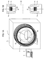
- the PET imaging apparatus of this embodiment is provided with a PET imaging apparatus 1, a bed 31 which holds an examinee H, a data processing apparatus (computer, etc.) 2 and a display apparatus 3.
- the PET imaging apparatus 1 includes many unit substrates U shown in Fig. 2 arranged in circumferential direction.
- the examinee H is laid on a bed 31 which is movable in the longitudinal direction and inserted into a measuring space 32 surrounded by the unit substrates U.
- the PET imaging apparatus l includes many unit substrates U arranged in the circumferential direction surrounding the measuring space 32 into which the bed 31 is inserted. A plurality of unit substrates U are also arranged in the longitudinal direction (axial direction of the measuring space 32) of the bed 31.
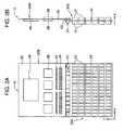
- the unit substrate U includes a radiation detection module (hereinafter referred to as “detection module”) 20A and an integrated circuit substrate (hereinafter referred to as "ASIC substrate”) 20B.
- the detection module 20A is provided with a plurality of semiconductor radiation detectors (hereinafter simply referred to as "detectors") 21.
- the detectors 21 detect ⁇ -rays emitted from within the body of the examinee H.
- the ASIC substrate 20B includes integrated circuits (ASIC) for measuring peak values and detection time of detected ⁇ -rays, designed to measure peak values and detection time of detected radiations ( ⁇ -rays).
- the integrated circuit includes a plurality of signal processing apparatuses which process radiation detection signals.
- the detector 21 includes a plurality of semiconductor radiation detector elements (hereinafter referred to as "detector elements,” see Fig. 3A) 211 including semiconductor regions (semiconductor sections) S, made up of a tabular semiconductor material, and conductive members (fixing members) 22, 23.
- the detector element 211 forms thin film-like electrodes on the two entire surfaces facing the semiconductor region S using a vapor deposition method, etc.
- the electrode formed on one surface is an anode electrode (first electrode, hereinafter referred to as "anode”) A and the electrode formed on the other surface is a cathode electrode (second electrode, hereinafter referred to as "cathode”) C.
- the detector 21 arranges an even number (e.g., four) of vertically positioned detector elements 211 in parallel in such a way that the cathodes C face each other and the anodes A face each other and the electrodes of the same type (the anodes A and cathodes C) are electrically connected through the conductive members 22, 23 (see Fig. 3B).
- the conductive member 23 (first conductive member) is interposed between the mutually facing anodes A of a pair of neighboring detector elements 211 and attached to the respective anodes A using a conductive adhesive 25.
- the conductive member 22 (second conductive member) is interposed between the mutually facing cathodes C of another pair of neighboring detector elements 211 and attached to the respective cathodes C using a conductive adhesive.
- the conductive members 22 are bonded to the respective cathodes C placed at both ends of the detector 21. In the detector 21, the anodes A and cathodes C are placed alternately and the conductive members 22 and conductive members 23 are also placed alternately.
- the semiconductor region S is a region which interacts with radiation to generate charge and is formed of any one single crystal of CdTe, CdZnTe, TlBr, GaAs, etc. Furthermore, for the cathode C and anode A, any one material of Pt, Au, In, etc., is used.
- the detector element 211 in this embodiment uses the cathode C whose principal ingredient is CdTe, Pt for the semiconductor region S and the anode A whose principal ingredient is In, forming a pn junction diode.
- bias voltage a backward bias voltage (hereinafter referred to as "bias voltage" of pn junction applied between the cathode C and anode A
- the semiconductor region S having a smaller t has a quicker rise of a peak value and has a higher degree of accuracy (energy resolution) of the peak value.
- the rising speed of the peak value is high, for example, the accuracy of simultaneous measurement (coincidence resolution) of the PET imaging apparatus 1 improves.
- the energy resolution of the semiconductor region S having a smaller thickness t increases (the efficiency of charge collection improves) because the time required for electrons to reach the anode A and the time required for holes to reach the cathode C are shortened, that is, the charge collection time is shortened. Furthermore, holes which are likely to be annihilated in midstream can reach the cathode C without being annihilated because of the small thickness.
- the thickness t can also be expressed as a distance between the mutually facing cathode C and anode A.
- the anode A is the electrode to extract a radiation detection signal and the cathode C is the electrode to apply a bias voltage.
- the thickness (distance between the electrodes) t of the semiconductor region S is preferably 0.2 mm to 2 mm. This is because when the thickness t exceeds 2 mm, the rising speed of a peak value slows down and a maximum value of the peak value also decreases. Even if the thickness t is increased, it is possible to increase the moving speed of electrons and holes by increasing the bias voltage and increasing the electric field strength in the thickness direction in the detector element 211 to thereby shorten the time for electrons and holes to reach the electrodes.
- increasing the bias voltage to be applied involves an increase in the size of a DC voltage power supply and may produce a harmful effect of causing dielectric breakdown inside the wiring board (support substrate) 24, and is therefore not preferable.
- the thickness (volume) of the electrodes (cathode C, anode A) relatively increases.
- this capacitance corresponds to an input capacitance component viewed from the signal processing circuit (ASIC) in the following stage, noise is more likely to occur in the signal processing circuit as the input capacitance increases and it is more likely to deteriorate energy resolution and coincidence resolution. Furthermore, securing the detection sensitivity per one detector 21 to a certain degree requires the volume of the detector 21 to be increased to a certain degree. For this purpose, the detector elements 211 are arranged in parallel to effectively secure the volume of the detector 21 as will be described later, but as the thickness t decreases, the number of elements to be arranged in parallel must be increased.
- the capacitance per one detector increases synergistically, causing deterioration in performance of the PET imaging apparatus 1 (deterioration in PET image contrast due to the deterioration in energy resolution, increase in the inspection time due to the deterioration of coincidence resolution or deterioration in image quality, etc.).
- the conductive members 22, 23 are flat plates of copper (or material whose principal ingredient is copper, for example, phosphor bronze) and have the same size as that of the respective electrodes of the detector element 211.
- the thickness of the conductive members 22, 23 is approximately 10 ⁇ m to 100 ⁇ m and preferably approximately 50 ⁇ m.
- the conductive member 22 includes a projection 22a (second electrical connection section) which protrudes outward from the semiconductor region S.
- the conductive member 23 includes a projection 23a (first electrical connection section) which protrudes outward from the semiconductor region S. More specifically, the projection 22a of the conductive member 22 connected to the cathode C is located on one side (left side in Fig. 3B) of the detector 21.
- the projection 23a of the conductive member 23 connected to the anode A is located on the other side facing the one side (right side in Fig. 3B) of the detector 21.
- the detector 21 is fixed to the wiring board 24 electrically connected thereto with three projections 22a and two projections 23a (see Fig. 3C).
- the conductive members 22, 23 also serve as fixing members to fix the detector 21 to the wiring board 24.
- the projections (electrical connection sections) 22a, 23a serve as the fixing sections to attach the detector 21 to the wiring board 24.
- Each detector 21 is disposed in such a way that the detector element 211 and the wiring board 24 cross each other, or more specifically cross each other at right angles, and is attached to the wiring board 24.
- the material of the conductive members 22, 23 is not limited to copper, but can also be aluminum or aluminum alloy and the shape thereof need not always be tabular. Furthermore, the size of the conductive members 22, 23 is preferably the same as the size of the electrodes of the detector element 211, but the size need not always be completely the same.
- each of the semiconductor regions S arranged in parallel has the aforementioned thickness t (0.2 to 2 mm).
- the thickness of the cathode C and anode A is approximately several ⁇ m at most. Since the cathodes C and anodes A of the plurality of detector elements 211 are connected together respectively, the detector 21 is not structured so as to identify the semiconductor region S of which detector element 211 interacts with ⁇ -rays. Such a structure of the detector 21 is intended to reduce the thickness t of the semiconductor region S (see Fig.
- the parallel arrangement of the semiconductor regions S is intended to reduce the amount of ⁇ -rays that pass through and increase interaction between the semiconductor regions S and ⁇ -rays (increase a ⁇ -ray count).
- the increase in the ⁇ -ray count leads to improve the sensitivity of the detector 21.
- the detector 21 is disposed on the wiring board 24 with a cathode connection member (e.g., printed wiring board pad) CP (second connection member) and an anode connection member AP (first connection member) provided on the surface of the wiring board 24 electrically connected to the projections 22a and projections 23a respectively using a conductive adhesive 25.
- the projections 22a, 23a also serve as electrical connection sections to be connected to the connection members CP, AP which are the conductive members provided on the wiring board 24.
- a plurality of connection members CP are disposed on the wiring board 24 as common connection members for a plurality of detectors 21.
- connection members CP (one connection member CP is not shown) are arranged in parallel in the Y direction (from left to right in Fig. 4A) of the wiring board 24. All the connection members CP are shortcircuited by wiring 24a which is buried in the wiring board 24 and given the same potential.
- the wiring 24a is connected to a terminal 33 provided at one end of the wiring board 24.
- connection members for each detector 21 are arranged in two rows between two neighboring connection members CP and disposed on the wiring board 24.
- a signal line (wiring) 24b buried in the wiring board 24 is connected to each connection member AP. This allows a ⁇ -ray detection signal of each detector 21 to be output through the corresponding signal line 24b.
- the respective signal lines 24b are individually connected to a plurality of terminals 34 provided at one end of the wiring board 24.
- a series of detectors 21 (six detectors 21) arranged in the Y direction are disposed in such a way that between the two adjacent neighboring detectors 21, the projections 23a, 23a of the respective conductive members 23 (connected to anodes A) face each other as shown in Fig. 4A.
- the projections 23a of the respective detectors 21 are attached to the corresponding connection members AP using the adhesive 25.
- the projections 22a of the respective detectors 21 are attached to the connection members CP using the adhesive 25.
- connection member CP1 In the two detectors 21 disposed on both sides of a connection member CP1 which is located in the center among the four connection members CP, the projections 23a of the respective conductive members 22 (connected to cathodes C) face each other. This allows the connection member CP1 to be shared by the detectors 21 (neighboring in the Y direction) disposed on both sides of the connection member CP1.
- thermoplastic adhesive for the adhesive 25.
- thermosetting adhesive which has the nature opposite to that of the thermoplastic adhesive so that these components are not separated. Selecting two different adhesives is useful because in the former, the part to which the adhesive 25 is applied is softened by overheat allowing the detector 21 to be removed easily, while in the latter, the detector element 211 and conductive members 22, 23 are hardly separated even if the detector element 211 is heated by a heat transfer.
- a bias voltage for charge collection e.g., a backward applied voltage such that the cathode C has -500 V and anode A has a potential close to ground potential, that is, the anode A has a potential 500 V higher than the potential of the cathode C
- a DC voltage power supply not shown
- holes corresponding to positive charge are attracted and moved to the cathode C, while electrons having negative charge are attracted and moved to the anode A.
- electrons have relatively greater mobility, and therefore electrons reach the anode A in a shorter time.
- holes have relatively smaller mobility, and therefore holes reach the cathode C in a relatively longer time. Holes may also be trapped before they reach the electrode.
- the conductive members 23 disposed between the anodes A, and the conductive members 22 disposed between the cathodes C constitute insensible regions where no ⁇ -rays are detected. Therefore, the detector 21 constructed in such a way that the conductive members 23, 22 constituting the insensible regions are disposed between the detector elements 211, or more specifically, between the electrodes. Both the anodes A and cathodes C are insensible regions.
- the detectors 21 are arranged on the wiring board 24 of the detection module 20A, six channels in the Y direction (radius direction of the PET imaging apparatus 1) from the detection module 20A to the ASIC substrate 20B, 16 channels in the X direction (circumferential direction of the PET imaging apparatus 1) orthogonal to the Y direction and two channels (both sides of the wiring board 24) in the Z direction (depth direction of the PET imaging apparatus 1) which is the thickness direction of the wiring board 24.
- a total of 96 channels of the detectors 21 are arranged on one side of the wiring board 24, a total of 192 channels on both sides.
- the detection module 20A can improve the arrangement density of the detectors 21 using the three structures as will be explained below.
- the respective detectors 21 are arranged in such a way that the projections 22a, 22b are oriented in the Y direction. This prevents the respective projections from being oriented in the X direction, and therefore it is possible to narrow gaps between the detectors 21 in the X direction.
- the respective detectors 21 are arranged in such a way that electrodes of the same polarity (e.g., cathode C) face each other in the X direction. This arrangement reduces insulation between the detectors 21 in the X direction, and can thereby narrow gaps between the detectors 21 in the X direction.
- the neighboring detectors 21 in the Y direction are arranged in such a way that the projections (parts of electrical connections with the outside of the detector) connected to the electrodes of the same polarity (anode A or cathode C) are arranged so as to face each other. This arrangement reduces insulation between the detectors 21 in the Y direction, and can thereby narrow gaps between the detectors 21 in the Y direction.
- the gaps between the detectors 21 in the X direction are narrow, and therefore when ⁇ -rays emitted from within the body of the examinee H on the bed 31 travel from bottom to top in Fig. 2A (Y direction, that is, radius direction of the PET imaging apparatus 1 (see Figs. 1A, 1B), it is possible to reduce the proportion of ⁇ -rays passing without being detected by the detectors 21 ( ⁇ -rays passing through gaps formed between the neighboring detectors 21). Therefore, the first and second structures increase the detection efficiency of ⁇ -rays and also improve spatial resolution of an image obtained. There is also an advantage of shortening an examination time.
- the gaps between the detectors 21 in the Y direction are narrow, and therefore the proportion of ⁇ -rays in the Y direction traveling askew with respect to the wiring board 24 that pass through the gaps between the detectors 21 in the Y direction is reduced. Therefore, this third structure as well as the first and second structures can increase the detection efficiency of ⁇ -rays and improve the spatial resolution of an image obtained. It also contributes to a reduction of the examination time.
- the detection module 20A having the first, second or third structure can increase the detection efficiency of ⁇ -rays and improve the spatial resolution of images.
- this embodiment arranges the detectors 21 on both sides of the wiring board 24, it is possible to reduce the number of wiring boards 24 arranged in the depth direction (Z direction) of the PET imaging apparatus 1 to half that in the case where the detectors 21 are only arranged on one side. This makes it possible to arrange the detectors 21 in the Z direction more densely. This embodiment also contributes to an increase in detection efficiency of ⁇ -rays and an improvement of spatial resolution of images in this case, too. It is also possible to further reduce the examination time. In addition, since the number of wiring boards 24 (unit substrates U) can be reduced by half as shown above, there is also a merit that it saves time and trouble in mounting the unit substrates U on the PET imaging apparatus 1 (see Fig. 1A, 1B).
- the detectors 21 are preferably coated with insulators to avoid dielectric breakdown.
- the insulator coats can be formed by immersing the unit including the entire detection module 20A in an insulator such as silicon rubber and then drying it to a thickness of several tens of microns.
- the detectors 21 excluding the projections 22a, 23a may be coated with the insulator first and then those projections 22a, 23a may be attached to the corresponding connection members of the wiring board 24.
- CP of the corresponding electrodes it is possible to make the conductive members 22, 23 smaller than the detector elements 211 so that portions of the projections 22a, 22b are disposed between the detector elements 211.
- the detectors 21 may also be adapted so that the areas of contact of the detector element 211 with the wiring board 24 may also be fixed to the wiring board 24 using an insulating adhesive.
- an insulating adhesive is preferably thermoplastic taking into account convertibility of the detectors 21.
- Fig. 5B it is also possible to further extend lower parts of the projections 22a, 23a of the conductive members 22, 23 downward to provide folded parts 22c, 23c and connect the folded parts 22c of the conductive members 22 to the connection member CP and connect the folded parts 23c of the conductive members 23 to the connection member AP as shown in Fig. 5A. It is possible to connect the folded parts 22c to the connection member CP and connect the folded parts 23c to the connection member AP using the adhesive 25. In this case, since contacts of the folded parts 22c, 23c with the connection member CP and connection member AP are surface-to-surface contacts, it is possible to fix the detectors 21 to the wiring board 24 more firmly.
- Fig. 6 it is also possible to share one conductive member 22 by cathodes C of the neighboring detectors 21 so as to integrate a plurality of detectors 21 into a one greater detector 21A.
- This structure can reduce the number of neighboring conductive members 22 of the neighboring detectors 21 by one for each pair in the X direction in Fig. 2A, increasing the number of detectors 21 in the X direction. Therefore, it is possible to realize high-density mounting of detectors 21 on the wiring board 24. Such mounting is feasible when there are an even number of detector elements 211 making up one detector 21 and the electrode disposed at one end at which the detectors 21 face each other is the cathode C.
- the unit substrate U is provided with the detection module 20A on which a plurality of detectors 21 are arranged as described above and an ASIC substrate 20B.
- the ASIC substrate 20B includes capacitors 26, resistors 27, analog ASICs 28 and a digital ASIC 29.
- the detection module 20A is constructed of a plurality of detectors 21 arranged on the wiring board 24.
- a voltage of, for example, 500 V is applied between the anode A and cathode C of the detector 21 for charge collection as described above.
- This voltage is applied between the anode A and cathode C of the respective detectors 21 from power supply wiring (not shown) set on the ASIC substrate 20B via a connector C1 and power supply wiring (not shown) set on the wiring board 24 of the detection module 20A.
- the detection module 20A is provided with the connector C1 at one end of the wiring board 24.
- the connector C1 includes the aforementioned terminal 33 and a plurality of terminal 34. ⁇ -ray detection signals output from the respective detectors 21 are supplied to the ASIC substrate 20B via the connector C1.
- the ASIC substrate 20B arranges four analog ASICs 28 and one digital ASIC 29 on one side of a wiring board (support substrate) 35.
- a wiring board (support substrate) 35 As shown in Fig. 2B, since the analog ASICs 28 are disposed on both sides of the wiring board 35, one ASIC substrate 20B includes a total of eight analog ASICs 28.
- capacitors 26 and resistors 27 as the detectors 21 are arranged on both sides of the wiring board 35.
- connection wires (not shown) inside the wiring board 35 for electrically connecting these capacitors 26, resistors 27, analog ASICs 28 and digital ASIC 29. These connection wires have a layered structure inside the wiring board 35.
- the arrangement of the capacitors 26, analog ASICs 28 and digital ASIC 29 on the wiring board 35 agrees with the order in which signals are supplied from the detectors 21 of the detection module 20A.
- One end of the resistor 27 is connected to the input side of the capacitor 26 and the other end is connected to ground wiring (not shown) provided on the wiring board 35.
- the analog ASIC 28 is an application-specific IC which processes analog signals ( ⁇ -ray detection signals) output from the detectors 21 and is a kind of an LSI.
- the analog ASIC 28 is provided with a signal processing circuit for each detector 21. These signal processing circuits are designed to receive a ⁇ -ray detection signal (radiation detection signal) output from the corresponding one detector 21 and calculate a ⁇ -ray peak value.
- the ASIC substrate 20B is provided with a connector (e.g., spring pin connector) C2 having a plurality of terminals connected to the respective capacitors 26 at one end of the wiring board 35.
- a connector e.g., spring pin connector
- the unit substrates U are arranged on a ring-shaped support member (not shown) provided on the PET imaging apparatus 1 in such a way that the surface on which the detectors 21 are arranged is oriented toward the depth direction (longitudinal direction of the bed 31 and Z direction in Fig. 2B) of the PET imaging apparatus 1.
- This ring-shaped support member is provided so as to surround the measuring space 32.
- the plurality of unit substrates U arranged on the ring-shaped member are disposed in the circumferential direction and surround the measuring space 32.
- the unit substrates U are arranged in such a way that the detection modules 20A are oriented inward (measuring space 32 side) and the ASIC substrates 20B are oriented outward.
- a plurality of unit substrates U are also arranged in the depth direction of the PET imaging apparatus 1.
- the orientation of the X direction shown in Fig. 2A, Fig. 3C, etc. is the circumferential direction (circumferential direction of the ring-shaped support member) of the PET imaging apparatus 1 and the orientation of the Y direction shown in Fig. 2A, Fig. 3C, etc., is the radius direction (radius direction of the ring-shaped support member) of the PET imaging apparatus 1.
- the ends of the detection module 20A and ASIC substrate 20B overlap with each other and the connector C1 and connector C2 which exist in this overlapped area are connected.
- the ends of the detection module 20A and ASIC substrate 20B are connected in a freely detachable (freely separable and connectable) manner using screws, etc., for clamping the overlapped area. They are connected in the overlapped area for the following reasons. That is, the unit substrate U consisting of the combined detection module 20A and ASIC substrate 20B is supported on one side inside the PET imaging apparatus 1, and therefore forces of deflecting or bending the unit substrate U act on the central part (connection section) of the unit substrate U depending on the installation position thereof.
- the connection section having a structure with the end faces of the wiring board 24 and wiring board 35 butt-contacted is likely to deflect or bend, and is therefore undesirable.
- this embodiment has the structure in which the detection module 20A and ASIC substrate 20B are connected in the overlapped area.
- the unit substrate U used in this embodiment improves toughness against deflection and bending compared to the connection of the wiring board 24 and wiring board 35, the ends of which are butt-contacted. Improving the toughness of the unit substrate U against deflection and bending suppresses, for example, dislocation of the detectors 21 and improves the accuracy of identifying positions at which ⁇ -rays occur.
- many unit substrates U are arranged in the PET imaging apparatus 1 in the circumferential direction and depth direction, and therefore the unit substrates U located at the lower part (especially the bottom) in Fig. 1A are likely to deflect or bend. For this reason, the toughness against deflection and bending of the unit substrates U constitutes an important factor.
- the detection module 20A is attached to the ASIC substrate 20B in a freely detachable manner using screws, etc., if problems like detection fault, etc., occurs in the detectors 21 and ASICs 28, 29, it is only necessary to replace parts with the problem (detection module 20A or ASIC substrate 20B). Moreover, since the detection module 20A and ASIC substrate 20B are electrically connected using the connector C1 such as the aforementioned spring pin connector, connection or disconnection (coupling or decoupling) between substrates is easy.
- one detection module 20A is connected to the ASIC substrate 20B, but the detection module 20A may be divided into plurality of portions.
- the detection module 20A may be divided into plurality of portions.
- this structure when one detector 21 malfunctions, it is only necessary to replace the one detection module mounted with the faulty detector out of the two detection modules, and thereby reduce waste (cost reduction) during maintenance.
- This structure makes it possible to shorten the length (distance) of wiring for transmitting feeble ⁇ -ray detection signals output from the detectors 21 to amplifiers of the analog ASICs. This reduces influences of noise on the ⁇ -ray detection signals and also reduces attenuation of the ⁇ -ray detection signals.
- capacitors 26 and resistors 27 are disposed outside the analog ASIC 28 in this embodiment.
- the capacitors 26, resistors 27 and analog ASICs 28 provided on the ASIC substrate 20B may also be provided on the detection module 20A instead of the ASIC substrate 20B.
- the capacitors 26, resistors 27 and analog ASICs 28 are arranged closer to the ASIC substrate 20B than the detectors 21. Since the detection module 20A includes the detectors 21 and analog ASICs 28, it is possible to further shorten the distance (length of wiring) between the detector 21 and analog ASIC 28. This further reduces influences of noise.
- radiopharmaceuticals e.g., containing 18 F
- Radiopharmaceuticals are administered to the examinee H using a method such as an injection so that radioactivity in the body becomes approximately 370 MBq.
- Radiopharmaceuticals are selected according to the purpose of inspection (to locate cancers or inspect pulmonary aneurysm of heart, etc.).
- the radiopharmaceuticals administered are soon concentrated on the affected area of the examinee H. In this condition, the examinee H is laid on the bed 31.
- the inspector who performs a PET inspection (clinical radiologic technologist or doctor) inputs necessary information (region whose tomogram is to be obtained (imaging region or region of concern), number of slices, slice interval, absorbed dose, etc.) through the data processing apparatus 2 (see Fig. 1A) according to the purpose of inspection.
- necessary information region whose tomogram is to be obtained (imaging region or region of concern), number of slices, slice interval, absorbed dose, etc.
- the bed 31 is moved in the longitudinal direction to insert the examinee H into the measuring space 32 until the region to be inspected (e.g., affected area of cancer) of the examinee H up to a predetermined position.
- the PET imaging apparatus 1 is activated.
- a DC high voltage is applied between the anode A and cathode C of the detector 21 and the PET imaging apparatus 1 starts a PET inspection.
- ⁇ -rays emitted from within the body of the examinee H provoked by radiopharmaceuticals are detected by the detectors 21. That is, a pair of ⁇ -rays are emitted in diametrically opposite directions at the time of annihilation of positrons emitted from the PET radiopharmaceuticals and detected by different detectors 21.
- the detectors 21 output ⁇ -ray detection signals. These detection signals are input to a signal processing circuit (not shown) inside the corresponding analog ASIC 28 via the signal lines 24b, connectors C1, C2 and capacitors 26.
- This signal processing circuit amplifies the ⁇ -ray detection signals and finds peak values of the detected ⁇ -rays. These peak values are converted to digital peak value information through an analog/digital converter (ADC) (not shown) in the digital ASIC 29.
- ADC analog/digital converter
- the digital ASIC 29 further outputs position information of the detectors 21 which have detected ⁇ -rays and information on the ⁇ -ray detection time.
- the digital peak value information, position information of the detectors 21 and information of the ⁇ -ray detection time are input to the data processing apparatus 2.
- a simultaneous measurement apparatus (not shown) of the data processing apparatus 2 counts a pair of ⁇ -rays generated by annihilation of one positron as one using the detection time information and identifies the positions of the detectors 21 which have detected the pair of ⁇ -rays based on the position information thereof. Furthermore, a tomogram information creation apparatus (not shown) which is the image information creation apparatus of the data processing apparatus 2 creates the position of accumulation of radiopharmaceuticals, that is, tomogram information (image information) of the examinee at the malignant tumor position using the count value obtained by simultaneous measurement and position information of the detectors 21. This tomogram information is displayed on the display apparatus 3.
- the PET imaging apparatus of this embodiment has a structure with the detectors 21 used for the PET imaging apparatus 1 shown in Fig. 1A, 1B replaced by detectors 21B shown in Figs. 7A, 7B.
- the structure of the PET imaging apparatus of this embodiment other than the detectors is the same as that of the PET imaging apparatus 1 shown in Fig. 1 which is the foregoing embodiment.
- the detector 21B used in this embodiment will be explained using Fig. 7A.
- the detectors 21B each consist of an even number of detector elements 211 arranged in parallel with mutually facing anodes A and mutually facing cathodes C.
- a conductive member 23A is interposed between the anodes A of the neighboring detector elements 211 and a conductive member 22A is interposed between the cathodes C of the neighboring detector elements 211.
- the conductive member 23A is attached to the anodes A of the neighboring detector elements 211 using a conductive adhesive.
- the conductive member 22A is attached to the cathodes C of the neighboring detector elements 211 using a conductive adhesive.
- the conductive member 22A is also attached to the cathodes C provided for the respective detector elements 211 at both ends of the detector 21B using a conductive adhesive.
- the conductive members 22A and 23A form projections 22b, 23b which protrude from the same side (plane facing the wiring board 24) toward the same direction.
- the projections 22b, 23b protrude outward from the semiconductor region S, that is, downward from the bottom (surface facing the wiring board 24) of the detector 21B.
- the projection 22b is located on one side of the detector element 211 and the projection 23b is located on the other side of the detector element 211 facing the one side.
- the respective projections 22b of the detector 21B are placed on the connection member CP and attached to the connection member CP using the adhesive 25. Furthermore, the respective projections 23b of the detector 21B are placed on the connection member AP and attached to the connection member AP using the adhesive 25. In this way, the detector 21B is attached to the wiring board 24.
- the respective semiconductor regions S of the detector 21B are arranged so as to cross the wiring board 24, or more specifically so as to cross at right angles. This embodiment also arranges a plurality of detectors 21B on the wiring board 24 as shown in Fig. 4A to form a detection module.
- This embodiment can produce the effects (1) to (7) and (9) to (20) of Embodiment 1 above. This embodiment further produces the following effects:
- Embodiment 2 in which the projections face each other refers to a state in which of the two sides of the neighboring detectors 21B in the Y direction crossing the surface of the detector 21B from which projection 22b protrudes at right angles, the sides on the projection 22b side face each other.
- Fig. 7C it is also possible to further extend the lower parts of the projections 22b, 23b of the conductive members 22A, 23A downward and form a folded parts 22d in the projection 22b and form a folded parts 23d in the projection 23b.
- the folded parts 22d is connected to the connection member CP and the folded parts 23d is connected to the connection member AP using the adhesive 2,5.
- Such connections of the folded parts 22d, 23d can realize enhanced fixing of the detectors 21 to the wiring board 24.
- one connection member AP per one detector 21 (or 21B) is provided on the wiring board 24.
- the respective projections 23a (or 23b) of one detector 21 (or 21B) are connected to different connection members AP using the adhesive 25.
- These connection members AP are connected to one signal line 24b inside the wiring board 24.
- Adopting such a structure can reduce the area of the connection members AP on the surface of the wiring board 24 (e.g., make the area equal to the cross-sectional area of the projection 23a (or 23b)) and can thereby prevent dielectric breakdown between the cathode C and conductive member 22 (or 22A) and connection member AP.
- Such a structure of the connection member AP is also applicable to the connection member CP. That is, as many different connection members CP as projections 22a (or 22b) of the respective detectors 21 (or 21B) connected to one connection member CP shown in Fig. 4A are arranged on one row on the wiring board 24. Then, the projections 22a (or 22b) corresponding to these connection members CP are connected separately using the adhesive 25.
- connection members CP are connected to one wiring 24a inside the wiring board 24.
- the connection member CP which connects the mutually facing projections 22a (or 22b) of the neighboring detectors 21 (or 21B) is disposed on the wiring board 24 one by one between the mutually facing projections 22a (or 22b).
- the area of the connection member CP on the surface of the wiring board 24 can also be reduced in the same way as the above-described connection member AP, and therefore it is possible to prevent dielectric breakdown between the anode A and conductive member 23 (or 23A) and connection member CP.
- connection member AP is provided for each projection 23a (or 23b) of the detector 21 (or 21B) and the connection member AP is provided for each projection 22a (or 22b) of the detector 21 (or 21B) on the wiring board 24.
- This structure is also applicable to the respective detection modules provided with detectors having the folded parts 22c, 23c shown in Fig. 5B and detectors having the folded parts 22d, 23d shown in Fig. 7C. In this case, it is preferably to determine the sizes of the folded parts 22c, 23c, 22d, 23d to sizes enough to hold the detectors 21.
- the projections 23a (or 23b) of the conductive members 23 (or 23A) connected to the anode A are connected to the connection member AP and the projection 22a (or 22b) of the conductive members 22 (or 22A) connected to the cathode C are connected to the connection member CP, but it is also possible to connect the projections 23a (or 23b) to the connection member CP and connect the projections 22a (or 22b) to the connection member AP.
- the cathode C becomes the electrode for outputting ⁇ -ray detection signals and the anode A becomes the electrode for applying a bias voltage. Any pattern can be realized if the voltage applied between the anode A and cathode C is at least a backward voltage.
- the potential of the anode A is set to substantially ground potential and the potential of the cathode C is set to -500 V, but there is no restriction on the potential if it is at least a backward one and it is possible to set a voltage value within a range in which the PET imaging apparatus functions. It is also possible to use the cathode C as the electrode for extracting radiation detection signals and use the anode A as the electrode for applying a bias voltage.
- Embodiments 1 and 2 arrange the cathodes C at both ends of the detector 21 (or 21B). However, it is also possible to arrange four detector elements 211 so that the anodes A are disposed at both ends of the detector 21 (or 21B). In this way, the cathodes C face each other at two locations and the anodes A face each other at one location in the detector.
- Embodiments 1 and 2 four detector elements 211 are arranged in parallel to form a detector 21, but the number of elements arranged in parallel is not limited to four. However, to improve electrical insulating properties in the X direction, it is preferable to construct one detector with an even number of detector elements 211.
- connection members AP and connection members CP on the wiring board 24 are also provided at locations other than areas where the adhesive 25 is connected.
- the area of these connection member AP and connection member CP can be limited to a minimum necessary area to which the adhesive 25 is connected and can be connected within the wiring board 24 if necessary. This makes it possible to enhance electrical insulating properties between the connection member AP, connection member CP and corresponding electrodes on the surface of the wiring board 24.
- the PET imaging apparatus see Fig. 1 as an example of radiological imaging apparatus
- the detector and detection module of the present invention are not limited to the PET imaging apparatus and can be applied to a SPECT (Single Photon Emission Computer Tomography) apparatus and ⁇ -camera.
- SPECT Single Photon Emission Computer Tomography
- a functional image obtained by a ⁇ -camera is two-dimensional and it is provided with a collimator for regulating the position of incidence (angle) of ⁇ -rays.
- Radiological imaging apparatus combining a PET imaging apparatus or SPECT apparatus with an X-ray CT.
Landscapes
- Physics & Mathematics (AREA)
- Health & Medical Sciences (AREA)
- Life Sciences & Earth Sciences (AREA)
- General Physics & Mathematics (AREA)
- High Energy & Nuclear Physics (AREA)
- Molecular Biology (AREA)
- Spectroscopy & Molecular Physics (AREA)
- Measurement Of Radiation (AREA)
- Light Receiving Elements (AREA)
- Nuclear Medicine (AREA)
- Solid State Image Pick-Up Elements (AREA)
- Transforming Light Signals Into Electric Signals (AREA)
Abstract
A radiation detection module (20A) and radiological imaging apparatus capable of improving spatial resolution. A semiconductor radiation detector (21) includes a plurality of semiconductor radiation detector elements (211) and conductive members (22, 23) which are copper plates. A detector element (211) provides an anode electrode (A) on one of facing sides of a semiconductor region (S) and a cathode electrode (C) on the other side. The respective detector elements (211) are arranged in parallel in such a way that the cathode electrodes (C) and anode electrodes (A) face each other respectively, and the anode electrodes (A) are electrically connected together and the cathode electrodes (C) are electrically connected together via the conductive members (22, 23) respectively. <IMAGE>
Description
The present invention relates to a radiation
detection module, radiation detector and radiological
imaging apparatus, and more particularly, to a
radiation detection module, radiation detector and
radiological imaging apparatus using semiconductor
radiation detector elements.
As an example of conventional radiation
detectors which detect radiation such as γ-rays, there
is a semiconductor radiation detector provided with a
semiconductor radiation detector element (hereinafter
referred to as "detector element") made of a
semiconductor material such as CdTe (cadmium
telluride), CdZnTe (cadmium zinc telluride), TlBr
(thallium bromide), GaAs (gallium arsenide). Since the
detector element converts charges produced by
interaction between radiation and the semiconductor
material to an electric signal, the semiconductor
radiation detector is characterized by higher
efficiency of conversion into an electric signal than a
radiation detector using a scintillator and its ability
to be miniaturized.
The semiconductor radiation detector is
provided with the aforementioned detector element and
electrodes formed on both surfaces facing this detector
element. By applying a DC high voltage between these
electrodes, the semiconductor radiation detector
collects charges generated when radiations such as X-rays,
γ-rays enter the detector element as signals from
the electrodes.
When the semiconductor radiation detector is
used for a medical radiation imaging apparatus
(radiological imaging apparatus), etc., a semiconductor
radiation detector is connected to a wiring board to
form a radiation detection section (e.g., see JP-A-2003-84068
(paragraph 0024, Fig. 3)). Furthermore, a
technology which arranges a plurality of semiconductor
radiation detectors on a radiation detector support
board is proposed (e.g., see JP-A-2003-167058
(paragraphs 0020 and 0021, Fig. 3)).
There is.a demand for a PET (Positron
Emission Tomography) apparatus which is a kind of
radiological imaging apparatus, with enhanced spatial
resolution to obtain images with a high degree of
accuracy. There is also a demand for a PET imaging
apparatus with improved γ-ray detection sensitivity, for
example, enhanced arrangement density of the radiation
detector in order to shorten inspection time. These
demands also apply to a SPECT (Single Photon Emission
Tomography) apparatus and other radiological imaging
apparatuses such as a γ-camera.
It is an object of the present invention to
provide a radiation detection module, radiation
detector and radiological imaging apparatus capable of
improving spatial resolution.
In order to attain the above-described
object, the radiation detector according to a first
invention comprises a plurality of radiation detector
elements including a semiconductor region, a first
electrode which collects a radiation detection signal
and a second electrode which applies a bias voltage,
both of which face each other with the semiconductor
region interposed in between, the semiconductor region
being disposed so as to cross a support substrate to
which the radiation detector is attached, wherein the
radiation detector elements are arranged with the
electrodes of the same type arranged in parallel facing
each other, conductive members are arranged between the
mutually facing electrodes of the same type and
attached to these electrodes and the conductive members
are attached to a first support substrate by being
connected to wiring provided for the first support
substrate.
In this way, the conductive members are used
as fixing members to attach the radiation detectors to
the support substrate. This eliminates the necessity
for any other fixing member to attach the radiation
detectors to the support substrate and can improve
arrangement density of radiation detectors on the
support substrate. This also leads to an improvement
in spatial resolution of an image obtained from the
examinee.
In a second invention, the support substrate
includes a plurality of first conductive connection
members to which a first conductive member, which is a
conductive member connected to a first electrode, is
attached and a plurality of conductive second
connection members to which a second conductive member,
which is a conductive member connected to a second
electrode, is attached, and the first connection
members are arranged in two parallel rows between the
second electrode connection members in one direction.
In this way, in the one direction, the respective first
conductive members connected to the electrodes of the
same type of the neighboring radiation detectors are
connected to the respective first connection members
arranged in two parallel rows between the second
electrode connection members. Therefore, it is
possible to reduce mutual electrical insulation among
the radiation detectors in the one direction and narrow
the distances among the radiation detectors in the one
direction. This also makes it possible to improve the
arrangement density of the radiation detectors on the
support substrate and to improve spatial resolution of
an image obtained.
The present invention can improve spatial
resolution.
Other objects, features and advantages of the
invention will become apparent from the following
description of the embodiments of the invention taken
in conjunction with the accompanying drawings.
Next, a PET imaging apparatus which is a
radiological imaging apparatus and a preferred
embodiment of the present invention will be explained
with reference to the attached drawings as appropriate
in detail below.
As shown in Fig. 1A, 1B, the PET imaging
apparatus of this embodiment is provided with a PET
imaging apparatus 1, a bed 31 which holds an examinee
H, a data processing apparatus (computer, etc.) 2 and a
display apparatus 3. The PET imaging apparatus 1
includes many unit substrates U shown in Fig. 2
arranged in circumferential direction. In the PET
imaging apparatus 1, the examinee H is laid on a bed 31
which is movable in the longitudinal direction and
inserted into a measuring space 32 surrounded by the
unit substrates U.
The PET imaging apparatus l includes many
unit substrates U arranged in the circumferential
direction surrounding the measuring space 32 into which
the bed 31 is inserted. A plurality of unit substrates
U are also arranged in the longitudinal direction
(axial direction of the measuring space 32) of the bed
31. As shown in Fig. 2A, 2B, the unit substrate U
includes a radiation detection module (hereinafter
referred to as "detection module") 20A and an
integrated circuit substrate (hereinafter referred to
as "ASIC substrate") 20B. The detection module 20A is
provided with a plurality of semiconductor radiation
detectors (hereinafter simply referred to as
"detectors") 21. The detectors 21 detect γ-rays emitted
from within the body of the examinee H. The ASIC
substrate 20B includes integrated circuits (ASIC) for
measuring peak values and detection time of detected γ-rays,
designed to measure peak values and detection
time of detected radiations (γ-rays). The integrated
circuit includes a plurality of signal processing
apparatuses which process radiation detection signals.
Next, details of the PET imaging apparatus 1
will be explained.
First, the detector 21 applied to this
embodiment will be explained first. As shown in Fig.
3B, the detector 21 includes a plurality of
semiconductor radiation detector elements (hereinafter
referred to as "detector elements," see Fig. 3A) 211
including semiconductor regions (semiconductor
sections) S, made up of a tabular semiconductor
material, and conductive members (fixing members) 22,
23. The detector element 211 forms thin film-like
electrodes on the two entire surfaces facing the
semiconductor region S using a vapor deposition method,
etc. The electrode formed on one surface is an anode
electrode (first electrode, hereinafter referred to as
"anode") A and the electrode formed on the other
surface is a cathode electrode (second electrode,
hereinafter referred to as "cathode") C. The detector
21 arranges an even number (e.g., four) of vertically
positioned detector elements 211 in parallel in such a
way that the cathodes C face each other and the anodes
A face each other and the electrodes of the same type
(the anodes A and cathodes C) are electrically
connected through the conductive members 22, 23 (see
Fig. 3B). That is, the conductive member 23 (first
conductive member) is interposed between the mutually
facing anodes A of a pair of neighboring detector
elements 211 and attached to the respective anodes A
using a conductive adhesive 25. The conductive member
22 (second conductive member) is interposed between the
mutually facing cathodes C of another pair of
neighboring detector elements 211 and attached to the
respective cathodes C using a conductive adhesive.
Furthermore, the conductive members 22 are bonded to
the respective cathodes C placed at both ends of the
detector 21. In the detector 21, the anodes A and
cathodes C are placed alternately and the conductive
members 22 and conductive members 23 are also placed
alternately.
The semiconductor region S is a region which
interacts with radiation to generate charge and is
formed of any one single crystal of CdTe, CdZnTe, TlBr,
GaAs, etc. Furthermore, for the cathode C and anode A,
any one material of Pt, Au, In, etc., is used. The
detector element 211 in this embodiment uses the
cathode C whose principal ingredient is CdTe, Pt for
the semiconductor region S and the anode A whose
principal ingredient is In, forming a pn junction
diode.
Here, a relationship between a time and peak
value curve when the thickness t (see Fig. 3A) of the
semiconductor region S is thick and thin will be
explained. When a backward bias voltage (hereinafter
referred to as "bias voltage") of pn junction applied
between the cathode C and anode A is the same, the
semiconductor region S having a smaller t has a quicker
rise of a peak value and has a higher degree of
accuracy (energy resolution) of the peak value. When
the rising speed of the peak value is high, for
example, the accuracy of simultaneous measurement
(coincidence resolution) of the PET imaging apparatus 1
improves. As the rising speed of the peak value
increases, the energy resolution of the semiconductor
region S having a smaller thickness t increases (the
efficiency of charge collection improves) because the
time required for electrons to reach the anode A and
the time required for holes to reach the cathode C are
shortened, that is, the charge collection time is
shortened. Furthermore, holes which are likely to be
annihilated in midstream can reach the cathode C
without being annihilated because of the small
thickness. The thickness t can also be expressed as a
distance between the mutually facing cathode C and
anode A. The anode A is the electrode to extract a
radiation detection signal and the cathode C is the
electrode to apply a bias voltage.
Furthermore, the thickness (distance between
the electrodes) t of the semiconductor region S is
preferably 0.2 mm to 2 mm. This is because when the
thickness t exceeds 2 mm, the rising speed of a peak
value slows down and a maximum value of the peak value
also decreases. Even if the thickness t is increased,
it is possible to increase the moving speed of
electrons and holes by increasing the bias voltage and
increasing the electric field strength in the thickness
direction in the detector element 211 to thereby
shorten the time for electrons and holes to reach the
electrodes. However, increasing the bias voltage to be
applied involves an increase in the size of a DC
voltage power supply and may produce a harmful effect
of causing dielectric breakdown inside the wiring board
(support substrate) 24, and is therefore not
preferable. On the other hand, when the thickness
falls below 0.2 mm, the thickness (volume) of the
electrodes (cathode C, anode A) relatively increases.
This results in a reduced proportion of the
semiconductor region S, which is the essential part
that interacts with radiations. That is, when the
thickness t of the semiconductor region S is reduced,
the thickness of the electrode that does not interact
with γ-rays, that is, the electrode (anode A and cathode
C) that does not detect γ-rays, relatively increases on
one hand, and the proportion of the semiconductor
region S that interacts with γ-rays relatively decreases
and the sensitivity of detecting γ-rays decreases as a
result. Furthermore, when the thickness t is small,
the capacitance per one detector element 211 increases.
Since this capacitance corresponds to an input
capacitance component viewed from the signal processing
circuit (ASIC) in the following stage, noise is more
likely to occur in the signal processing circuit as the
input capacitance increases and it is more likely to
deteriorate energy resolution and coincidence
resolution. Furthermore, securing the detection
sensitivity per one detector 21 to a certain degree
requires the volume of the detector 21 to be increased
to a certain degree. For this purpose, the detector
elements 211 are arranged in parallel to effectively
secure the volume of the detector 21 as will be
described later, but as the thickness t decreases, the
number of elements to be arranged in parallel must be
increased. As a result, the capacitance per one
detector increases synergistically, causing
deterioration in performance of the PET imaging
apparatus 1 (deterioration in PET image contrast due to
the deterioration in energy resolution, increase in the
inspection time due to the deterioration of coincidence
resolution or deterioration in image quality, etc.).
The conductive members 22, 23 are flat plates
of copper (or material whose principal ingredient is
copper, for example, phosphor bronze) and have the same
size as that of the respective electrodes of the
detector element 211. The thickness of the conductive
members 22, 23 is approximately 10 µm to 100 µm and
preferably approximately 50 µm. The conductive member
22 includes a projection 22a (second electrical
connection section) which protrudes outward from the
semiconductor region S. The conductive member 23
includes a projection 23a (first electrical connection
section) which protrudes outward from the semiconductor
region S. More specifically, the projection 22a of the
conductive member 22 connected to the cathode C is
located on one side (left side in Fig. 3B) of the
detector 21. The projection 23a of the conductive
member 23 connected to the anode A is located on the
other side facing the one side (right side in Fig. 3B)
of the detector 21. The detector 21 is fixed to the
wiring board 24 electrically connected thereto with
three projections 22a and two projections 23a (see Fig.
3C). Thus, the conductive members 22, 23 also serve as
fixing members to fix the detector 21 to the wiring
board 24. Especially, the projections (electrical
connection sections) 22a, 23a serve as the fixing
sections to attach the detector 21 to the wiring board
24. Each detector 21 is disposed in such a way that
the detector element 211 and the wiring board 24 cross
each other, or more specifically cross each other at
right angles, and is attached to the wiring board 24.
The material of the conductive members 22, 23 is not
limited to copper, but can also be aluminum or aluminum
alloy and the shape thereof need not always be tabular.
Furthermore, the size of the conductive members 22, 23
is preferably the same as the size of the electrodes of
the detector element 211, but the size need not always
be completely the same.
In the detector 21, each of the semiconductor
regions S arranged in parallel has the aforementioned
thickness t (0.2 to 2 mm). The thickness of the
cathode C and anode A is approximately several µm at
most. Since the cathodes C and anodes A of the
plurality of detector elements 211 are connected
together respectively, the detector 21 is not
structured so as to identify the semiconductor region S
of which detector element 211 interacts with γ-rays.
Such a structure of the detector 21 is intended to
reduce the thickness t of the semiconductor region S
(see Fig. 3A), increase the charge collection
efficiency, increase the rising speed of peak values,
increase energy resolution, and at the same time the
parallel arrangement of the semiconductor regions S is
intended to reduce the amount of γ-rays that pass
through and increase interaction between the
semiconductor regions S and γ-rays (increase a γ-ray
count). The increase in the γ-ray count leads to
improve the sensitivity of the detector 21. Of course,
it is also possible to adopt a structure that allows
radiation to be identified for each detector element
211.
As shown in Fig. 3C, the detector 21 is
disposed on the wiring board 24 with a cathode
connection member (e.g., printed wiring board pad) CP
(second connection member) and an anode connection
member AP (first connection member) provided on the
surface of the wiring board 24 electrically connected
to the projections 22a and projections 23a respectively
using a conductive adhesive 25. The projections 22a,
23a also serve as electrical connection sections to be
connected to the connection members CP, AP which are
the conductive members provided on the wiring board 24.
As shown in Fig. 4, a plurality of connection members
CP are disposed on the wiring board 24 as common
connection members for a plurality of detectors 21.
The four connection members CP (one connection member
CP is not shown) are arranged in parallel in the Y
direction (from left to right in Fig. 4A) of the wiring
board 24. All the connection members CP are shortcircuited
by wiring 24a which is buried in the wiring
board 24 and given the same potential. The wiring 24a
is connected to a terminal 33 provided at one end of
the wiring board 24.
As the connection members for each detector
21, the connection members AP are arranged in two rows
between two neighboring connection members CP and
disposed on the wiring board 24. A signal line
(wiring) 24b buried in the wiring board 24 is connected
to each connection member AP. This allows a γ-ray
detection signal of each detector 21 to be output
through the corresponding signal line 24b. The
respective signal lines 24b are individually connected
to a plurality of terminals 34 provided at one end of
the wiring board 24.
In this embodiment, a series of detectors 21
(six detectors 21) arranged in the Y direction are
disposed in such a way that between the two adjacent
neighboring detectors 21, the projections 23a, 23a of
the respective conductive members 23 (connected to
anodes A) face each other as shown in Fig. 4A. In such
a condition, as shown in Fig. 3C, the projections 23a
of the respective detectors 21 are attached to the
corresponding connection members AP using the adhesive
25. Furthermore, the projections 22a of the respective
detectors 21 are attached to the connection members CP
using the adhesive 25. In the two detectors 21
disposed on both sides of a connection member CP1 which
is located in the center among the four connection
members CP, the projections 23a of the respective
conductive members 22 (connected to cathodes C) face
each other. This allows the connection member CP1 to
be shared by the detectors 21 (neighboring in the Y
direction) disposed on both sides of the connection
member CP1.
As the adhesive 25, conductive paste and
solder, etc., can be used. Considering the convenience
in the case of removing a faulty detector 21 due to
malfunction, etc., from the wiring board 24, it is
preferable to use a thermoplastic adhesive for the
adhesive 25. On the other hand, for bonding between
the detector element 211 and conductive members 22, 23,
it is preferable to use a thermosetting adhesive which
has the nature opposite to that of the thermoplastic
adhesive so that these components are not separated.
Selecting two different adhesives is useful because in
the former, the part to which the adhesive 25 is
applied is softened by overheat allowing the detector
21 to be removed easily, while in the latter, the
detector element 211 and conductive members 22, 23 are
hardly separated even if the detector element 211 is
heated by a heat transfer.
Here, an overview of the principles of
detection of γ-rays by the detector 21 will be
explained. When γ-rays enter the detector 21 from the Y
direction and γ-rays interact with the semiconductor
regions S, pairs of holes and electrons are produced in
quantities proportional to the energy of γ-rays. Here,
a bias voltage for charge collection (e.g., a backward
applied voltage such that the cathode C has -500 V and
anode A has a potential close to ground potential, that
is, the anode A has a potential 500 V higher than the
potential of the cathode C) is applied between the
cathode C and anode A of the detector 21 from a DC
voltage power supply (not shown). For this reason,
holes corresponding to positive charge are attracted
and moved to the cathode C, while electrons having
negative charge are attracted and moved to the anode A.
When these holes and electrons are compared, electrons
have relatively greater mobility, and therefore
electrons reach the anode A in a shorter time. On the
other hand, holes have relatively smaller mobility, and
therefore holes reach the cathode C in a relatively
longer time. Holes may also be trapped before they
reach the electrode.
The conductive members 23 disposed between
the anodes A, and the conductive members 22 disposed
between the cathodes C constitute insensible regions
where no γ-rays are detected. Therefore, the detector
21 constructed in such a way that the conductive
members 23, 22 constituting the insensible regions are
disposed between the detector elements 211, or more
specifically, between the electrodes. Both the anodes
A and cathodes C are insensible regions.
As shown in Figs. 2A, 2B, the detectors 21
are arranged on the wiring board 24 of the detection
module 20A, six channels in the Y direction (radius
direction of the PET imaging apparatus 1) from the
detection module 20A to the ASIC substrate 20B, 16
channels in the X direction (circumferential direction
of the PET imaging apparatus 1) orthogonal to the Y
direction and two channels (both sides of the wiring
board 24) in the Z direction (depth direction of the
PET imaging apparatus 1) which is the thickness
direction of the wiring board 24. In this way, a total
of 96 channels of the detectors 21 are arranged on one
side of the wiring board 24, a total of 192 channels on
both sides.
As the arrangement density of the detectors
21 arranged on the detection module 20A increases, it
becomes easier to detect γ-rays and it is possible to
increase the positional accuracy when detecting γ-rays.
The detection module 20A according to this embodiment
can improve the arrangement density of the detectors 21
using the three structures as will be explained below.
In a first structure, the respective detectors 21 are
arranged in such a way that the projections 22a, 22b
are oriented in the Y direction. This prevents the
respective projections from being oriented in the X
direction, and therefore it is possible to narrow gaps
between the detectors 21 in the X direction. In a
second structure, the respective detectors 21 are
arranged in such a way that electrodes of the same
polarity (e.g., cathode C) face each other in the X
direction. This arrangement reduces insulation between
the detectors 21 in the X direction, and can thereby
narrow gaps between the detectors 21 in the X
direction. Furthermore, in a third structure, the
neighboring detectors 21 in the Y direction are
arranged in such a way that the projections (parts of
electrical connections with the outside of the
detector) connected to the electrodes of the same
polarity (anode A or cathode C) are arranged so as to
face each other. This arrangement reduces insulation
between the detectors 21 in the Y direction, and can
thereby narrow gaps between the detectors 21 in the Y
direction.
According to the first and second structures,
the gaps between the detectors 21 in the X direction
are narrow, and therefore when γ-rays emitted from
within the body of the examinee H on the bed 31 travel
from bottom to top in Fig. 2A (Y direction, that is,
radius direction of the PET imaging apparatus 1 (see
Figs. 1A, 1B), it is possible to reduce the proportion
of γ-rays passing without being detected by the
detectors 21 (γ-rays passing through gaps formed between
the neighboring detectors 21). Therefore, the first
and second structures increase the detection efficiency
of γ-rays and also improve spatial resolution of an
image obtained. There is also an advantage of
shortening an examination time. Furthermore, according
to the third structure, the gaps between the detectors
21 in the Y direction are narrow, and therefore the
proportion of γ-rays in the Y direction traveling askew
with respect to the wiring board 24 that pass through
the gaps between the detectors 21 in the Y direction is
reduced. Therefore, this third structure as well as
the first and second structures can increase the
detection efficiency of γ-rays and improve the spatial
resolution of an image obtained. It also contributes
to a reduction of the examination time.
Thus, the detection module 20A having the
first, second or third structure can increase the
detection efficiency of γ-rays and improve the spatial
resolution of images.
Since this embodiment arranges the detectors
21 on both sides of the wiring board 24, it is possible
to reduce the number of wiring boards 24 arranged in
the depth direction (Z direction) of the PET imaging
apparatus 1 to half that in the case where the
detectors 21 are only arranged on one side. This makes
it possible to arrange the detectors 21 in the Z
direction more densely. This embodiment also
contributes to an increase in detection efficiency of γ-rays
and an improvement of spatial resolution of images
in this case, too. It is also possible to further
reduce the examination time. In addition, since the
number of wiring boards 24 (unit substrates U) can be
reduced by half as shown above, there is also a merit
that it saves time and trouble in mounting the unit
substrates U on the PET imaging apparatus 1 (see Fig.
1A, 1B).
The detectors 21 are preferably coated with
insulators to avoid dielectric breakdown. The
insulator coats can be formed by immersing the unit
including the entire detection module 20A in an
insulator such as silicon rubber and then drying it to
a thickness of several tens of microns. In this case,
the detectors 21 excluding the projections 22a, 23a may
be coated with the insulator first and then those
projections 22a, 23a may be attached to the
corresponding connection members of the wiring board
24. In order to reduce the danger of dielectric
breakdown between the conductive members 22, 23 and the
connection members AP, CP of the corresponding
electrodes, it is possible to make the conductive
members 22, 23 smaller than the detector elements 211
so that portions of the projections 22a, 22b are
disposed between the detector elements 211.
Furthermore, the detectors 21 may also be
adapted so that the areas of contact of the detector
element 211 with the wiring board 24 may also be fixed
to the wiring board 24 using an insulating adhesive.
Such a structure strengthens bonding, that is, holding
power of the wiring board 24 to the detector 21. In
this case, the insulating adhesive is preferably
thermoplastic taking into account convertibility of the
detectors 21.
Furthermore, as shown in Fig. 5B, it is also
possible to further extend lower parts of the
projections 22a, 23a of the conductive members 22, 23
downward to provide folded parts 22c, 23c and connect
the folded parts 22c of the conductive members 22 to
the connection member CP and connect the folded parts
23c of the conductive members 23 to the connection
member AP as shown in Fig. 5A. It is possible to
connect the folded parts 22c to the connection member
CP and connect the folded parts 23c to the connection
member AP using the adhesive 25. In this case, since
contacts of the folded parts 22c, 23c with the
connection member CP and connection member AP are
surface-to-surface contacts, it is possible to fix the
detectors 21 to the wiring board 24 more firmly.
Furthermore, as shown in Fig. 6, it is also
possible to share one conductive member 22 by cathodes
C of the neighboring detectors 21 so as to integrate a
plurality of detectors 21 into a one greater detector
21A. This structure can reduce the number of
neighboring conductive members 22 of the neighboring
detectors 21 by one for each pair in the X direction in
Fig. 2A, increasing the number of detectors 21 in the X
direction. Therefore, it is possible to realize high-density
mounting of detectors 21 on the wiring board
24. Such mounting is feasible when there are an even
number of detector elements 211 making up one detector
21 and the electrode disposed at one end at which the
detectors 21 face each other is the cathode C.
A detailed structure of the unit substrate U
will be explained using Figs. 2A, 2B. The unit
substrate U is provided with the detection module 20A
on which a plurality of detectors 21 are arranged as
described above and an ASIC substrate 20B. The ASIC
substrate 20B includes capacitors 26, resistors 27,
analog ASICs 28 and a digital ASIC 29.
As shown in Fig. 4, the detection module 20A
is constructed of a plurality of detectors 21 arranged
on the wiring board 24. A voltage of, for example, 500
V is applied between the anode A and cathode C of the
detector 21 for charge collection as described above.
This voltage is applied between the anode A and cathode
C of the respective detectors 21 from power supply
wiring (not shown) set on the ASIC substrate 20B via a
connector C1 and power supply wiring (not shown) set on
the wiring board 24 of the detection module 20A. The
detection module 20A is provided with the connector C1
at one end of the wiring board 24. The connector C1
includes the aforementioned terminal 33 and a plurality
of terminal 34. γ-ray detection signals output from the
respective detectors 21 are supplied to the ASIC
substrate 20B via the connector C1.
As shown in Figs. 2A, 2B, the ASIC substrate
20B arranges four analog ASICs 28 and one digital ASIC
29 on one side of a wiring board (support substrate)
35. As shown in Fig. 2B, since the analog ASICs 28 are
disposed on both sides of the wiring board 35, one ASIC
substrate 20B includes a total of eight analog ASICs
28. As many capacitors 26 and resistors 27 as the
detectors 21 are arranged on both sides of the wiring
board 35. Furthermore, there are a plurality of
connection wires (not shown) inside the wiring board 35
for electrically connecting these capacitors 26,
resistors 27, analog ASICs 28 and digital ASIC 29.
These connection wires have a layered structure inside
the wiring board 35. The arrangement of the capacitors
26, analog ASICs 28 and digital ASIC 29 on the wiring
board 35 agrees with the order in which signals are
supplied from the detectors 21 of the detection module
20A. One end of the resistor 27 is connected to the
input side of the capacitor 26 and the other end is
connected to ground wiring (not shown) provided on the
wiring board 35. The analog ASIC 28 is an application-specific
IC which processes analog signals (γ-ray
detection signals) output from the detectors 21 and is
a kind of an LSI. The analog ASIC 28 is provided with
a signal processing circuit for each detector 21.
These signal processing circuits are designed to
receive a γ-ray detection signal (radiation detection
signal) output from the corresponding one detector 21
and calculate a γ-ray peak value.
The ASIC substrate 20B is provided with a
connector (e.g., spring pin connector) C2 having a
plurality of terminals connected to the respective
capacitors 26 at one end of the wiring board 35.
The unit substrates U are arranged on a ring-shaped
support member (not shown) provided on the PET
imaging apparatus 1 in such a way that the surface on
which the detectors 21 are arranged is oriented toward
the depth direction (longitudinal direction of the bed
31 and Z direction in Fig. 2B) of the PET imaging
apparatus 1. This ring-shaped support member is
provided so as to surround the measuring space 32. The
plurality of unit substrates U arranged on the ring-shaped
member are disposed in the circumferential
direction and surround the measuring space 32. The
unit substrates U are arranged in such a way that the
detection modules 20A are oriented inward (measuring
space 32 side) and the ASIC substrates 20B are oriented
outward. According to this embodiment, a plurality of
unit substrates U are also arranged in the depth
direction of the PET imaging apparatus 1. In the unit
substrates U arranged as described above, the
orientation of the X direction shown in Fig. 2A, Fig.
3C, etc., is the circumferential direction
(circumferential direction of the ring-shaped support
member) of the PET imaging apparatus 1 and the
orientation of the Y direction shown in Fig. 2A, Fig.
3C, etc., is the radius direction (radius direction of
the ring-shaped support member) of the PET imaging
apparatus 1.
As shown in Fig. 2B, the ends of the
detection module 20A and ASIC substrate 20B overlap
with each other and the connector C1 and connector C2
which exist in this overlapped area are connected. The
ends of the detection module 20A and ASIC substrate 20B
are connected in a freely detachable (freely separable
and connectable) manner using screws, etc., for
clamping the overlapped area. They are connected in
the overlapped area for the following reasons. That
is, the unit substrate U consisting of the combined
detection module 20A and ASIC substrate 20B is
supported on one side inside the PET imaging apparatus
1, and therefore forces of deflecting or bending the
unit substrate U act on the central part (connection
section) of the unit substrate U depending on the
installation position thereof. The connection section
having a structure with the end faces of the wiring
board 24 and wiring board 35 butt-contacted is likely
to deflect or bend, and is therefore undesirable.
On the basis of this point, this embodiment
has the structure in which the detection module 20A and
ASIC substrate 20B are connected in the overlapped
area. Thus, the unit substrate U used in this
embodiment improves toughness against deflection and
bending compared to the connection of the wiring board
24 and wiring board 35, the ends of which are butt-contacted.
Improving the toughness of the unit
substrate U against deflection and bending suppresses,
for example, dislocation of the detectors 21 and
improves the accuracy of identifying positions at which
γ-rays occur. As shown in Fig. 1A, many unit substrates
U are arranged in the PET imaging apparatus 1 in the
circumferential direction and depth direction, and
therefore the unit substrates U located at the lower
part (especially the bottom) in Fig. 1A are likely to
deflect or bend. For this reason, the toughness
against deflection and bending of the unit substrates U
constitutes an important factor.
Using such an electrical connection structure
of the detection module 20A and ASIC substrate 20B
using the connector C1 and connector C2 allows γ-ray
detection signals to be transmitted from the detection
module 20A to the ASIC substrate 20B with low losses.
With reduced losses, the energy resolution of the
detectors 21 improves, for example.
Since the detection module 20A is attached to
the ASIC substrate 20B in a freely detachable manner
using screws, etc., if problems like detection fault,
etc., occurs in the detectors 21 and ASICs 28, 29, it
is only necessary to replace parts with the problem
(detection module 20A or ASIC substrate 20B).
Moreover, since the detection module 20A and ASIC
substrate 20B are electrically connected using the
connector C1 such as the aforementioned spring pin
connector, connection or disconnection (coupling or
decoupling) between substrates is easy.
In the above-described structure, one
detection module 20A is connected to the ASIC substrate
20B, but the detection module 20A may be divided into
plurality of portions. For example, it is possible to
connect two detection modules to the ASIC substrate,
each substrate mounted with eight detectors 21 in the
horizontal direction and six detectors 21 in the
vertical direction. According to this structure, when
one detector 21 malfunctions, it is only necessary to
replace the one detection module mounted with the
faulty detector out of the two detection modules, and
thereby reduce waste (cost reduction) during
maintenance. Instead of dividing the unit substrate U
into the detection module 20A and ASIC substrate 20B,
it is also possible to mount a plurality of detectors
21, capacitors 26, resistors 27 and analog ASICs 28 and
one digital ASIC substrate on one wiring board. This
structure eliminates the necessity for the connectors
C1, C2.
The shorter the length of the circuit and
wiring length (distance) of transmitting a γ-ray
detection signal, the better, because there is less
influence of noise and less attenuation of signals in
midstream. Furthermore, when simultaneous measurement
processing is performed using the PET imaging apparatus
1, a shorter circuit or shorter wiring is preferable
because it results in a smaller time delay (preferable
because the accuracy of the detection time is not
reduced). For this reason, in this embodiment, the
detectors 21, capacitors 26, analog ASICs 28 and
digital ASIC 29 are arranged on the unit substrate U in
that order from the central axis to the outside in the
radius direction of the PET imaging apparatus 1. This
structure makes it possible to shorten the length
(distance) of wiring for transmitting feeble γ-ray
detection signals output from the detectors 21 to
amplifiers of the analog ASICs. This reduces
influences of noise on the γ-ray detection signals and
also reduces attenuation of the γ-ray detection signals.
Furthermore, it is also possible to arrange
the capacitors 26 and resistors 27 inside the analog
ASIC 28, but for reasons of obtaining appropriate
capacitance and appropriate resistance values and
reducing the size of the analog ASIC 28, the capacitors
26 and resistors 27 are disposed outside the analog
ASIC 28 in this embodiment.
The capacitors 26, resistors 27 and analog
ASICs 28 provided on the ASIC substrate 20B may also be
provided on the detection module 20A instead of the
ASIC substrate 20B. In this case, the capacitors 26,
resistors 27 and analog ASICs 28 are arranged closer to
the ASIC substrate 20B than the detectors 21. Since
the detection module 20A includes the detectors 21 and
analog ASICs 28, it is possible to further shorten the
distance (length of wiring) between the detector 21 and
analog ASIC 28. This further reduces influences of
noise.
The operation of the PET imaging apparatus 1
structured as above will be explained. Before starting
a radiation inspection, radiopharmaceuticals (e.g.,
containing 18F) for the PET are administered to the
examinee H using a method such as an injection so that
radioactivity in the body becomes approximately 370
MBq. Radiopharmaceuticals are selected according to
the purpose of inspection (to locate cancers or inspect
pulmonary aneurysm of heart, etc.). The
radiopharmaceuticals administered are soon concentrated
on the affected area of the examinee H. In this
condition, the examinee H is laid on the bed 31.
The inspector who performs a PET inspection
(clinical radiologic technologist or doctor) inputs
necessary information (region whose tomogram is to be
obtained (imaging region or region of concern), number
of slices, slice interval, absorbed dose, etc.) through
the data processing apparatus 2 (see Fig. 1A) according
to the purpose of inspection. In this case, it is
possible to display an information input screen (not
shown) on the display apparatus 3 and input necessary
data using a keyboard or mouse, etc. Then, the bed 31
is moved in the longitudinal direction to insert the
examinee H into the measuring space 32 until the region
to be inspected (e.g., affected area of cancer) of the
examinee H up to a predetermined position. Then, the
PET imaging apparatus 1 is activated.
According to an instruction from the data
processing apparatus 2, a DC high voltage is applied
between the anode A and cathode C of the detector 21
and the PET imaging apparatus 1 starts a PET
inspection. γ-rays emitted from within the body of the
examinee H provoked by radiopharmaceuticals are
detected by the detectors 21. That is, a pair of γ-rays
are emitted in diametrically opposite directions at the
time of annihilation of positrons emitted from the PET
radiopharmaceuticals and detected by different
detectors 21. The detectors 21 output γ-ray detection
signals. These detection signals are input to a signal
processing circuit (not shown) inside the corresponding
analog ASIC 28 via the signal lines 24b, connectors C1,
C2 and capacitors 26. This signal processing circuit
amplifies the γ-ray detection signals and finds peak
values of the detected γ-rays. These peak values are
converted to digital peak value information through an
analog/digital converter (ADC) (not shown) in the
digital ASIC 29. The digital ASIC 29 further outputs
position information of the detectors 21 which have
detected γ-rays and information on the γ-ray detection
time. The digital peak value information, position
information of the detectors 21 and information of the
γ-ray detection time are input to the data processing
apparatus 2. A simultaneous measurement apparatus (not
shown) of the data processing apparatus 2 counts a pair
of γ-rays generated by annihilation of one positron as
one using the detection time information and identifies
the positions of the detectors 21 which have detected
the pair of γ-rays based on the position information
thereof. Furthermore, a tomogram information creation
apparatus (not shown) which is the image information
creation apparatus of the data processing apparatus 2
creates the position of accumulation of
radiopharmaceuticals, that is, tomogram information
(image information) of the examinee at the malignant
tumor position using the count value obtained by
simultaneous measurement and position information of
the detectors 21. This tomogram information is
displayed on the display apparatus 3.
The effects produced in this embodiment will
be explained below.
A PET imaging apparatus which is another
embodiment of the present invention will be explained.
The PET imaging apparatus of this embodiment has a
structure with the detectors 21 used for the PET
imaging apparatus 1 shown in Fig. 1A, 1B replaced by
detectors 21B shown in Figs. 7A, 7B. The structure of
the PET imaging apparatus of this embodiment other than
the detectors is the same as that of the PET imaging
apparatus 1 shown in Fig. 1 which is the foregoing
embodiment.
The detector 21B used in this embodiment will
be explained using Fig. 7A. Like the detectors 21, the
detectors 21B each consist of an even number of
detector elements 211 arranged in parallel with
mutually facing anodes A and mutually facing cathodes
C. A conductive member 23A is interposed between the
anodes A of the neighboring detector elements 211 and a
conductive member 22A is interposed between the
cathodes C of the neighboring detector elements 211.
The conductive member 23A is attached to the anodes A
of the neighboring detector elements 211 using a
conductive adhesive. The conductive member 22A is
attached to the cathodes C of the neighboring detector
elements 211 using a conductive adhesive. The
conductive member 22A is also attached to the cathodes
C provided for the respective detector elements 211 at
both ends of the detector 21B using a conductive
adhesive.
The conductive members 22A and 23A form
projections 22b, 23b which protrude from the same side
(plane facing the wiring board 24) toward the same
direction. The projections 22b, 23b protrude outward
from the semiconductor region S, that is, downward from
the bottom (surface facing the wiring board 24) of the
detector 21B. The projection 22b is located on one
side of the detector element 211 and the projection 23b
is located on the other side of the detector element
211 facing the one side.
As shown in Fig. 7B, the respective
projections 22b of the detector 21B are placed on the
connection member CP and attached to the connection
member CP using the adhesive 25. Furthermore, the
respective projections 23b of the detector 21B are
placed on the connection member AP and attached to the
connection member AP using the adhesive 25. In this
way, the detector 21B is attached to the wiring board
24. The respective semiconductor regions S of the
detector 21B are arranged so as to cross the wiring
board 24, or more specifically so as to cross at right
angles. This embodiment also arranges a plurality of
detectors 21B on the wiring board 24 as shown in Fig.
4A to form a detection module.
This embodiment can produce the effects (1)
to (7) and (9) to (20) of Embodiment 1 above. This
embodiment further produces the following effects:
The arrangement in Embodiment 2 in which the
projections face each other refers to a state in which
of the two sides of the neighboring detectors 21B in
the Y direction crossing the surface of the detector
21B from which projection 22b protrudes at right
angles, the sides on the projection 22b side face each
other.
As shown in Fig. 7C, it is also possible to
further extend the lower parts of the projections 22b,
23b of the conductive members 22A, 23A downward and
form a folded parts 22d in the projection 22b and form
a folded parts 23d in the projection 23b. In this
case, the folded parts 22d is connected to the
connection member CP and the folded parts 23d is
connected to the connection member AP using the
adhesive 2,5. Such connections of the folded parts 22d,
23d can realize enhanced fixing of the detectors 21 to
the wiring board 24. Furthermore, it is also possible
to provide a concave section (groove) (not shown)
whereby the projections 22b, 23b are fitted into the
wiring board 24, fit the projections 22b, 23b into the
concave section and fix the detector 21B to the wiring
board 24.
In the aforementioned Embodiments 1 and 2,
one connection member AP per one detector 21 (or 21B)
is provided on the wiring board 24. However, it is
also possible to provide a different connection member
AP to the wiring board 24 for each projection 23a (or
23b) of the detector 21 (or 21B). In this case, the
respective projections 23a (or 23b) of one detector 21
(or 21B) are connected to different connection members
AP using the adhesive 25. These connection members AP
are connected to one signal line 24b inside the wiring
board 24. Adopting such a structure can reduce the
area of the connection members AP on the surface of the
wiring board 24 (e.g., make the area equal to the
cross-sectional area of the projection 23a (or 23b))
and can thereby prevent dielectric breakdown between
the cathode C and conductive member 22 (or 22A) and
connection member AP. Such a structure of the
connection member AP is also applicable to the
connection member CP. That is, as many different
connection members CP as projections 22a (or 22b) of
the respective detectors 21 (or 21B) connected to one
connection member CP shown in Fig. 4A are arranged on
one row on the wiring board 24. Then, the projections
22a (or 22b) corresponding to these connection members
CP are connected separately using the adhesive 25.
These connection members CP are connected to one wiring
24a inside the wiring board 24. However, the
connection member CP which connects the mutually facing
projections 22a (or 22b) of the neighboring detectors
21 (or 21B) is disposed on the wiring board 24 one by
one between the mutually facing projections 22a (or
22b). Furthermore, the area of the connection member
CP on the surface of the wiring board 24 can also be
reduced in the same way as the above-described
connection member AP, and therefore it is possible to
prevent dielectric breakdown between the anode A and
conductive member 23 (or 23A) and connection member CP.
In the above-described structure, the
connection member AP is provided for each projection
23a (or 23b) of the detector 21 (or 21B) and the
connection member AP is provided for each projection
22a (or 22b) of the detector 21 (or 21B) on the wiring
board 24. This structure is also applicable to the
respective detection modules provided with detectors
having the folded parts 22c, 23c shown in Fig. 5B and
detectors having the folded parts 22d, 23d shown in
Fig. 7C. In this case, it is preferably to determine
the sizes of the folded parts 22c, 23c, 22d, 23d to
sizes enough to hold the detectors 21.
In Embodiments 1 and 2, the projections 23a
(or 23b) of the conductive members 23 (or 23A)
connected to the anode A are connected to the
connection member AP and the projection 22a (or 22b) of
the conductive members 22 (or 22A) connected to the
cathode C are connected to the connection member CP,
but it is also possible to connect the projections 23a
(or 23b) to the connection member CP and connect the
projections 22a (or 22b) to the connection member AP.
In this case, the cathode C becomes the electrode for
outputting γ-ray detection signals and the anode A
becomes the electrode for applying a bias voltage. Any
pattern can be realized if the voltage applied between
the anode A and cathode C is at least a backward
voltage.
In Embodiments 1 and 2, the potential of the
anode A is set to substantially ground potential and
the potential of the cathode C is set to -500 V, but
there is no restriction on the potential if it is at
least a backward one and it is possible to set a
voltage value within a range in which the PET imaging
apparatus functions. It is also possible to use the
cathode C as the electrode for extracting radiation
detection signals and use the anode A as the electrode
for applying a bias voltage.
Embodiments 1 and 2 arrange the cathodes C at
both ends of the detector 21 (or 21B). However, it is
also possible to arrange four detector elements 211 so
that the anodes A are disposed at both ends of the
detector 21 (or 21B). In this way, the cathodes C face
each other at two locations and the anodes A face each
other at one location in the detector.
In Embodiments 1 and 2, four detector
elements 211 are arranged in parallel to form a
detector 21, but the number of elements arranged in
parallel is not limited to four. However, to improve
electrical insulating properties in the X direction, it
is preferable to construct one detector with an even
number of detector elements 211.
In Embodiments 1 and 2, as shown in Fig. 3C,
Fig. 4A, Fig. 5A, Fig. 6 and Fig. 7B, the connection
members AP and connection members CP on the wiring
board 24 are also provided at locations other than
areas where the adhesive 25 is connected. The area of
these connection member AP and connection member CP can
be limited to a minimum necessary area to which the
adhesive 25 is connected and can be connected within
the wiring board 24 if necessary. This makes it
possible to enhance electrical insulating properties
between the connection member AP, connection member CP
and corresponding electrodes on the surface of the
wiring board 24.
The foregoing embodiments have explained the
PET imaging apparatus (see Fig. 1) as an example of
radiological imaging apparatus, but the detector and
detection module of the present invention are not
limited to the PET imaging apparatus and can be applied
to a SPECT (Single Photon Emission Computer Tomography)
apparatus and γ-camera. It is a point common to the PET
imaging apparatus and SPECT apparatus that a three-dimensional
functional image of an examinee is taken,
but the SPECT apparatus is based on a principle of
measurement for detecting single photons, and therefore
it cannot perform simultaneous measurement and is
provided with a collimator for regulating the position
of incidence (angle) of γ-rays. Furthermore, a
functional image obtained by a γ-camera is two-dimensional
and it is provided with a collimator for
regulating the position of incidence (angle) of γ-rays.
It is also possible to construct a
radiological imaging apparatus combining a PET imaging
apparatus or SPECT apparatus with an X-ray CT.
It should be further understood by those
skilled in the art that although the foregoing
description has been made on embodiments of the
invention, the invention is not limited thereto and
various changes and modifications may be made without
departing from the spirit of the invention and the
scope of the appended claims.
Claims (33)
- A radiation detection module (20A) comprising at least one radiation detector and a support substrate to which said radiation detector is attached,
wherein said radiation detector comprises a plurality of radiation detector elements including a semiconductor region (S), a first electrode which collects a radiation detection signal and a second electrode which applies a bias voltage, both of which face each other with said semiconductor region (S) interposed in between, said semiconductor region (S) being disposed so as to cross said support substrate, and a plurality of conductive members (22, 23),
said plurality of radiation detector elements are arranged with said electrodes of the same type arranged in parallel facing each other, some of said plurality of conductive members (22, 23) are arranged between said electrodes of the same type facing each other and attached to these electrodes and the rest of said conductive members (22, 23) are attached to said first electrode or said second electrode which is singly disposed, and
said conductive members (22, 23) are attached to said support substrate and connected to wiring provided for said support substrate. - The radiation detection module (20A) according to claim 1, wherein said conductive members (22, 23) are fixing members for fixing said radiation detectors to said support substrate.
- The radiation detection module (20A) according to claim 1, wherein some of said conductive members (22, 23) are attached to said first electrode and other said conductive members (22, 23) are attached to said second electrode through a conductive adhesive (25).
- The radiation detection module (20A) according to claim 3, wherein said conductive adhesive (25) is a thermosetting adhesive (25).
- The radiation detection module (20A) according to claim 1, wherein each of said conductive members (22, 23) includes an electrical connection section which protrudes outward from said semiconductor region (S) and which forms part of said conductive member, and the structure of attaching said conductive member to said support substrate is realized by attaching said electrical connection section to said support substrate.
- The radiation detection module (20A) according to claim 5, wherein the position at which said electrical connection section protrudes differs between said conductive member connected to said first electrode and said other conductive member connected to said second electrode.
- The radiation detection module (20A) according to claim 6, wherein said electrical connection section of said conductive member connected to said first electrode protrudes on one side of said radiation detector and said electrical connection section of said conductive member connected to said second electrode protrudes on the other side of said radiation detector facing said one side.
- The radiation detection module (20A) according to claim 6, wherein said electrical connection section of said conductive member connected to said first electrode and said electrical connection section of said conductive member connected to said second electrode protrude at different positions on the surface of said radiation detector facing said support substrate.
- The radiation detection module (20A) according to claim 1, wherein said conductive members (22, 23) are attached to said first electrode or said second electrode so as to substantially cover the corresponding electrode surface.
- The radiation detection module (20A) according to claim 9, wherein said conductive member is a tabular member.
- The radiation detection module (20A) according to claim 1, wherein the plurality of said radiation detectors are arranged on said support substrate so that the electrical connection sections connected to electrodes of the same type substantially face each other in one direction.
- The radiation detection module (20A) according to claim 1, wherein the plurality of said radiation detectors are arranged on said support substrate so that the electrodes of the same type face each other in a direction perpendicular to said one direction.
- The radiation detection module (20A) according to claim 1, wherein said conductive members (22, 23) are conductive members (22, 23) having rigidity.
- A radiation detection module (20A) comprising at least one radiation detector and a support substrate provided with said radiation detector,
wherein said radiation detector comprises a plurality of radiation detector elements including a semiconductor region (S), a first electrode which collects a radiation detection signal and a second electrode which applies a bias voltage, both of which face each other with said semiconductor region (S) interposed in between, said semiconductor region (S) being disposed so as to cross said support substrate, and a plurality of conductive members (22, 23),
said plurality of radiation detector elements are arranged with said electrodes of the same type arranged in parallel facing each other, some of said plurality of conductive members (22, 23) are arranged between said electrodes of the same type facing each other and attached to these electrodes and the rest of said conductive members (22, 23) are attached to said first electrode or said second electrode which is singly disposed,
said support substrate includes a plurality of conductive first connection members (AP, CP) to which first conductive members (22, 23) which are said conductive members (22, 23) connected to said first electrode are attached, and a plurality of conductive second connection members (AP, CP) to which second conductive members (22, 23) which are said conductive members (22, 23) connected to said second electrode are attached,
said first connection members (AP, CP) are arranged in two parallel rows between said second connection members (AP, CP) in one direction, and
a plurality of first wires connected separately to said plurality of first connection members (AP, CP) are provided on said support substrate and a second wire connected to said plurality of second connection members (AP, CP) and shared by said plurality of second connection members (AP, CP) is provided on said support substrate. - The radiation detection module (20A) according to claim 14, wherein said first conductive members (22, 23) are attached to said first connection members (AP, CP) and said second conductive members (22, 23) are attached to said second connection members (AP, CP) using a conductive adhesive (25).
- The radiation detection module (20A) according to claim 15, wherein said conductive adhesive (25) is solder or thermoplastic adhesive (25).
- The radiation detection module (20A) according to claim 14, wherein said first connection member is provided for each of said first conductive members (22, 23) and said second connection member is provided for each of a pair of said mutually facing second conductive members (22, 23) on said neighboring radiation detectors in said one direction.
- The radiation detection module (20A) according to claim 14, wherein said first connection member is provided for each of said radiation detectors and said second connection member is provided so that said second conductive members (22, 23) of the plurality of said radiation detectors arranged in a direction perpendicular to said one direction are connected thereto.
- The radiation detection module (20A) according to claim 14, wherein said first conductive member includes a first electrical connection section which protrudes outward from said semiconductor region (S) and which forms part of said first conductive member, said second conductive member includes a second electrical connection section which protrudes outward from said semiconductor region (S) and which forms part of said second conductive member, said first electrical connection section is attached to said first connection member and said second electrical connection section is attached to said second connection member.
- A radiation detector comprising:wherein said plurality of radiation detector elements are arranged in parallel with said electrodes of the same type placed facing each other,a semiconductor region (S);a plurality of radiation detector elements having a first electrode which collects a radiation detection signal and a second electrode which applies a bias voltage, both of which face each other with said semiconductor region (S) interposed in between; anda plurality of metallic conductive members (22, 23),
some of said plurality of conductive members (22, 23) are arranged between mutually facing electrodes of the same type and attached to these electrodes and the rest of said conductive members (22, 23) are attached to said first electrode or said second electrode which is singly disposed without facing each other, and
said each conductive member includes an electrical connection section which forms part of said conductive member and which protrudes outward from said semiconductor region (S) so as to serve as a fixing member for attaching said conductive member to other members. - The radiation detector according to claim 20, wherein the position at which said electrical connection section protrudes differs between said conductive member connected to said first electrode and said other conductive member connected to said second electrode.
- The radiation detector according to claim 21, wherein said electrical connection section of said conductive member connected to said first electrode protrudes on one side of said radiation detector and said electrical connection section of said conductive member connected to said second electrode protrudes on the other side of said radiation detector which faces said one side.
- The radiation detector according to claim 21, wherein said electrical connection section of said conductive member connected to said first electrode and said electrical connection section of said conductive member connected to said second electrode protrude at different positions on one surface of said semiconductor region (S) on which neither first electrode nor second electrode is provided.
- The radiation detector according to claim 20, wherein said conductive members (22, 23) are attached to said first electrode or said second electrode so as to substantially cover the corresponding electrode surface.
- A radiological imaging apparatus comprising:wherein said radiation detector comprises a plurality of radiation detector elements including a semiconductor region (S), a first electrode which collects a radiation detection signal and a second electrode which applies a bias voltage, both of which face each other with said semiconductor region (S) interposed in between, said semiconductor region (S) being disposed so as to cross said support substrate, and a plurality of conductive members (22, 23),a plurality of radiation detection modules (20A) having a plurality of radiation detectors and a first support substrate provided with said radiation detectors, surrounding a bed which holds an examinee (H) and arranged around said bed; andan image information creation apparatus which creates images using information obtained based on radiation detection signals output from said radiation detectors,
said plurality of radiation detector elements are arranged with said electrodes of the same type arranged in parallel facing each other, some of said plurality of conductive members (22, 23) are arranged between said electrodes of the same type facing each other and attached to these electrodes and the rest of said conductive members (22, 23) are attached to said first electrode or said second electrode which is singly disposed, and
said conductive members (22, 23) are attached to said first support substrate and connected to a wire provided on said first support substrate. - The radiological imaging apparatus according to claim 25, wherein each of said conductive members (22, 23) includes an electrical connection section which protrudes outward from said semiconductor region (S) and which forms part of said conductive member and the structure of attaching said conductive member to said support substrate is realized by attaching said electrical connection section to said support substrate.
- The radiological imaging apparatus according to claim 25, wherein the surface of said first support substrate to which said radiation detectors are attached is oriented in the longitudinal direction of said bed.
- The radiological imaging apparatus according to claim 25, further comprising a signal processing unit including a second support substrate attached to said first support substrate in a freely detachable manner and an integrated circuit including a plurality of signal processing apparatuses which process radiation detection signals output from the plurality of said radiation detectors.
- A radiological imaging apparatus comprising:wherein said radiation detector comprises a plurality of radiation detector elements including a semiconductor region (S), a first electrode which collects a radiation detection signal and a second electrode which applies a bias voltage, both of which face each other with said semiconductor region (S) interposed in between, said semiconductor region (S) being disposed so as to cross said support substrate, and a plurality of conductive members (22, 23),a plurality of radiation detection modules 20A having a plurality of radiation detectors and a first support substrate provided with said radiation detectors, surrounding a bed which holds an examinee (H) and arranged around said bed; andan image information creation apparatus which creates images using information obtained based on a radiation detection signal output from said radiation detector,
said plurality of radiation detector elements are arranged with said electrodes of the same type arranged in parallel facing each other, some of said plurality of conductive members (22, 23) are arranged between said electrodes of the same type facing each other and attached to these electrodes and the rest of said conductive members (22, 23) are attached to said first electrode or said second electrode which is singly disposed,
said first support substrate comprises a plurality of first conductive connection members (AP, CP) to which first conductive members (22, 23) which are said conductive members (22, 23) connected to said first electrode are attached and a plurality of second conductive connection members (AP, CP) to which second conductive members (22, 23) which are said conductive members (22, 23) connected to said second electrode are attached,
said first connection members (AP, CP) are arranged in two parallel rows between said second electrode connection members (AP, CP) in one direction, and
a plurality of first wires connected to said plurality of first connection members (AP, CP) separately are provided on said first support substrate and second wires connected to said plurality of second connection members (AP, CP) and shared by said plurality of second connection members (AP, CP) are provided on said first support substrate. - The radiological imaging apparatus according to claim 29, wherein said first conductive member includes a first electrical connection section which protrudes outward from said semiconductor region (S) and which forms part of said first conductive member,
said second conductive member includes a second electrical connection section which protrudes outward from said semiconductor region (S) and which forms part of said second conductive member, and
said first electric connection section is attached to said first connection member and said second electrical connection section is attached to said second connection member. - The radiological imaging apparatus according to claim 29, wherein the surface of said first support substrate on which said radiation detectors are attached is oriented in the longitudinal direction of said bed.
- The radiological imaging apparatus according to claim 29, further comprising a signal processing unit including a second support substrate attached to said first support substrate in a freely detachable manner and an integrated circuit including a plurality of signal processing apparatuses which process radiation detection signals output from the plurality of said radiation detectors.
- A radiological imaging apparatus comprising:wherein said radiation detector comprises a plurality of radiation detector elements including a semiconductor region (S), a first electrode which collects a radiation detection signal and a second electrode which applies a bias voltage, both of which face each other with said semiconductor region (S) interposed in between, said semiconductor region (S) being disposed so as to cross said support substrate, and a plurality of conductive members (22, 23),a plurality of radiation detector;an integrated circuit which processes radiation detection signals output from a plurality of said radiation detectors;a support substrate to which said radiation detectors and said integrated circuit are attached;a plurality of unit substrates (U) surrounding a bed which holds an examinee (H) and arranged around said bed; andan image information creation apparatus which creates images using information obtained based on a radiation detection signal output from said integrated circuit,
said plurality of radiation detector elements are arranged with said electrodes of the same type arranged in parallel facing each other, some of said plurality of conductive members (22, 23) are arranged between said electrodes of the same type facing each other and attached to these electrodes and the rest of said conductive members (22, 23) are attached to said first electrode or said second electrode which is singly disposed.
Applications Claiming Priority (2)
| Application Number | Priority Date | Filing Date | Title |
|---|---|---|---|
| JP2004068954 | 2004-03-11 | ||
| JP2004068954A JP3828896B2 (en) | 2004-03-11 | 2004-03-11 | Positron emission tomography system |
Publications (1)
| Publication Number | Publication Date |
|---|---|
| EP1574877A1 true EP1574877A1 (en) | 2005-09-14 |
Family
ID=34824604
Family Applications (1)
| Application Number | Title | Priority Date | Filing Date |
|---|---|---|---|
| EP05005277A Withdrawn EP1574877A1 (en) | 2004-03-11 | 2005-03-10 | Radiation detection module, radiation detector and radiological imaging apparatus |
Country Status (3)
| Country | Link |
|---|---|
| US (1) | US7247860B2 (en) |
| EP (1) | EP1574877A1 (en) |
| JP (1) | JP3828896B2 (en) |
Cited By (2)
| Publication number | Priority date | Publication date | Assignee | Title |
|---|---|---|---|---|
| CN101604023B (en) * | 2008-06-12 | 2012-11-14 | 清华大学 | Array solid probe for radiation detection |
| CN114188581A (en) * | 2021-11-11 | 2022-03-15 | 广东泰极动力科技有限公司 | CCM cathode and anode automatic identification system, method, equipment and storage medium |
Families Citing this family (22)
| Publication number | Priority date | Publication date | Assignee | Title |
|---|---|---|---|---|
| JP2005223009A (en) * | 2004-02-03 | 2005-08-18 | Hitachi Ltd | Semiconductor radiation detector and radiation detection apparatus |
| JP3852858B1 (en) | 2005-08-16 | 2006-12-06 | 株式会社日立製作所 | Semiconductor radiation detector, radiation detection module and nuclear medicine diagnostic apparatus |
| JP3858044B1 (en) * | 2005-09-09 | 2006-12-13 | 株式会社日立製作所 | Radiation detection module, printed circuit board, and positron emission tomography apparatus |
| JP4834427B2 (en) * | 2006-03-06 | 2011-12-14 | 株式会社日立製作所 | Radiation detection module, printed circuit board, and nuclear medicine diagnostic apparatus |
| JP4619985B2 (en) * | 2006-04-28 | 2011-01-26 | 住友重機械工業株式会社 | Radiation detector and radiation inspection apparatus |
| JP4834467B2 (en) * | 2006-06-15 | 2011-12-14 | 株式会社日立製作所 | Printed circuit board mounting structure and nuclear medicine diagnostic apparatus |
| JP4695578B2 (en) * | 2006-09-29 | 2011-06-08 | 株式会社日立製作所 | Semiconductor radiation detector and positron emission tomography system |
| US7462833B2 (en) | 2007-04-17 | 2008-12-09 | Redlen Technologies | Multi-functional cathode packaging design for solid-state radiation detectors |
| US7955992B2 (en) | 2008-08-08 | 2011-06-07 | Redlen Technologies, Inc. | Method of passivating and encapsulating CdTe and CZT segmented detectors |
| US9202961B2 (en) | 2009-02-02 | 2015-12-01 | Redlen Technologies | Imaging devices with solid-state radiation detector with improved sensitivity |
| US8614423B2 (en) | 2009-02-02 | 2013-12-24 | Redlen Technologies, Inc. | Solid-state radiation detector with improved sensitivity |
| DE102009015563B4 (en) * | 2009-03-30 | 2018-02-22 | Siemens Healthcare Gmbh | X-ray detector for the detection of ionizing radiation, in particular for use in a CT system |
| FR2948200B1 (en) * | 2009-07-16 | 2013-02-08 | Commissariat Energie Atomique | RADIATION DETECTION DEVICE WITH IMPROVED ARRANGEMENT |
| JP5450188B2 (en) * | 2010-03-16 | 2014-03-26 | 株式会社東芝 | Radiation detection apparatus, method for manufacturing radiation detection apparatus, and image capturing apparatus |
| JP5714255B2 (en) * | 2010-08-02 | 2015-05-07 | 日立アロカメディカル株式会社 | Radiation detection unit |
| JP5753802B2 (en) * | 2012-01-27 | 2015-07-22 | 株式会社日立製作所 | Semiconductor radiation detector and nuclear medicine diagnostic equipment |
| US12298454B2 (en) | 2015-08-10 | 2025-05-13 | Shanghai United Imaging Healthcare Co., Ltd. | Apparatus and method for PET detector |
| US9696439B2 (en) | 2015-08-10 | 2017-07-04 | Shanghai United Imaging Healthcare Co., Ltd. | Apparatus and method for PET detector |
| US10070748B2 (en) | 2016-09-08 | 2018-09-11 | Kenney Manufacturing Co. | Curtain rod bracket and cam lock |
| US11002302B2 (en) | 2016-09-08 | 2021-05-11 | Kenney Manufacturing Company | Rod bracket |
| US12193588B1 (en) | 2018-03-19 | 2025-01-14 | Kenney Manufacturing Company | Fast fit bracket |
| US11835666B1 (en) * | 2020-07-31 | 2023-12-05 | Redlen Technologies, Inc. | Photon counting computed tomography detector with improved count rate stability and method of operating same |
Citations (3)
| Publication number | Priority date | Publication date | Assignee | Title |
|---|---|---|---|---|
| US4700076A (en) * | 1983-09-02 | 1987-10-13 | Digital Imaging Company Of America, Inc. | Solid-state X-ray receptor and method of making same |
| EP0642178A2 (en) * | 1993-08-31 | 1995-03-08 | Seiko Instruments Inc. | Semiconductor device for converting light and radiations into electricity |
| JPH11304930A (en) * | 1998-04-15 | 1999-11-05 | Japan Energy Corp | 2D matrix array radiation detector |
Family Cites Families (15)
| Publication number | Priority date | Publication date | Assignee | Title |
|---|---|---|---|---|
| JPS60196692A (en) | 1984-03-20 | 1985-10-05 | Hitachi Medical Corp | Radiation detector |
| US4937453A (en) * | 1987-05-06 | 1990-06-26 | Nelson Robert S | X-ray detector for radiographic imaging |
| JP3427584B2 (en) | 1995-03-22 | 2003-07-22 | 三菱電機株式会社 | Wide-area radiation detector |
| US6235051B1 (en) | 1997-12-16 | 2001-05-22 | Timothy P. Murphy | Method of stent-graft system delivery |
| JPH11337646A (en) | 1998-05-29 | 1999-12-10 | Toshiba Corp | Radiation semiconductor detector, radiation semiconductor detector array, and collimator installation device |
| US6236051B1 (en) * | 1998-03-27 | 2001-05-22 | Kabushiki Kaisha Toshiba | Semiconductor radiation detector |
| JPH11281747A (en) | 1998-03-27 | 1999-10-15 | Toshiba Corp | Radiation semiconductor detector |
| IL143980A0 (en) * | 2001-06-25 | 2002-04-21 | Imarad Imaging Systems Ltd | Three dimensional radiation detection |
| JP2003084068A (en) | 2001-09-12 | 2003-03-19 | Toshiba Corp | Radiation detector and manufacturing method thereof |
| JP3820972B2 (en) | 2001-12-03 | 2006-09-13 | 株式会社日立製作所 | PET equipment |
| JP2003218505A (en) | 2002-01-17 | 2003-07-31 | Matsushita Electric Ind Co Ltd | Printed circuit board, printed circuit board unit, method of inspecting and manufacturing printed circuit board unit, and communication device using printed circuit board unit |
| JP2005109269A (en) * | 2003-09-30 | 2005-04-21 | Hitachi Ltd | Semiconductor radiation detector and semiconductor radiation imaging apparatus |
| JP4594624B2 (en) * | 2004-01-13 | 2010-12-08 | 株式会社日立製作所 | Radiation detection device and nuclear medicine diagnostic device |
| JP3852850B2 (en) * | 2004-10-25 | 2006-12-06 | 株式会社日立製作所 | Radiation imaging apparatus and nuclear medicine diagnostic apparatus |
| JP3792708B1 (en) * | 2005-02-22 | 2006-07-05 | 株式会社日立製作所 | Nuclear medicine diagnostic apparatus and positron emission tomography apparatus |
-
2004
- 2004-03-11 JP JP2004068954A patent/JP3828896B2/en not_active Expired - Fee Related
-
2005
- 2005-03-10 US US11/075,769 patent/US7247860B2/en not_active Expired - Lifetime
- 2005-03-10 EP EP05005277A patent/EP1574877A1/en not_active Withdrawn
Patent Citations (3)
| Publication number | Priority date | Publication date | Assignee | Title |
|---|---|---|---|---|
| US4700076A (en) * | 1983-09-02 | 1987-10-13 | Digital Imaging Company Of America, Inc. | Solid-state X-ray receptor and method of making same |
| EP0642178A2 (en) * | 1993-08-31 | 1995-03-08 | Seiko Instruments Inc. | Semiconductor device for converting light and radiations into electricity |
| JPH11304930A (en) * | 1998-04-15 | 1999-11-05 | Japan Energy Corp | 2D matrix array radiation detector |
Non-Patent Citations (1)
| Title |
|---|
| PATENT ABSTRACTS OF JAPAN vol. 2000, no. 02 29 February 2000 (2000-02-29) * |
Cited By (3)
| Publication number | Priority date | Publication date | Assignee | Title |
|---|---|---|---|---|
| CN101604023B (en) * | 2008-06-12 | 2012-11-14 | 清华大学 | Array solid probe for radiation detection |
| CN114188581A (en) * | 2021-11-11 | 2022-03-15 | 广东泰极动力科技有限公司 | CCM cathode and anode automatic identification system, method, equipment and storage medium |
| CN114188581B (en) * | 2021-11-11 | 2023-09-29 | 广东泰极动力科技有限公司 | CCM cathode and anode automatic identification system, method, equipment and storage medium |
Also Published As
| Publication number | Publication date |
|---|---|
| JP3828896B2 (en) | 2006-10-04 |
| US7247860B2 (en) | 2007-07-24 |
| US20050230630A1 (en) | 2005-10-20 |
| JP2005257437A (en) | 2005-09-22 |
Similar Documents
| Publication | Publication Date | Title |
|---|---|---|
| US7247860B2 (en) | Radiation detection module, radiation detector and radiological imaging apparatus | |
| JP3858044B1 (en) | Radiation detection module, printed circuit board, and positron emission tomography apparatus | |
| US7615757B2 (en) | Semiconductor radiological detector and semiconductor radiological imaging apparatus | |
| US7297955B2 (en) | Semiconductor radiation detector, positron emission tomography apparatus, semiconductor radiation detection apparatus, detector unit and nuclear medicine diagnostic apparatus | |
| US7582879B2 (en) | Modular x-ray measurement system | |
| JP4594624B2 (en) | Radiation detection device and nuclear medicine diagnostic device | |
| RU2647206C1 (en) | Sensor device and visualization system for detecting radiation signals | |
| CN107850678B (en) | Detector unit for detector array of radiation imaging modality device | |
| US20100308230A1 (en) | Detector array substrate and nuclear medicine diagnosis device using same | |
| JP3852858B1 (en) | Semiconductor radiation detector, radiation detection module and nuclear medicine diagnostic apparatus | |
| US20130049151A1 (en) | Anode-illuminated radiation detector | |
| US7138632B2 (en) | Radiation detector | |
| US20090072159A1 (en) | Semiconductor detection module and radiation detection apparatus and radiological imaging apparatus using the semiconductor detection module | |
| JP4834427B2 (en) | Radiation detection module, printed circuit board, and nuclear medicine diagnostic apparatus | |
| JP5136736B2 (en) | Radiation image detection module and radiation image detection apparatus | |
| JP4641211B2 (en) | Radiation detector and radiation inspection apparatus | |
| JP2006300551A (en) | Radiation detection circuit, radiation detector, and radiation inspection apparatus | |
| JP2007052004A (en) | Semiconductor radiation detector, radiation detection module and nuclear medicine diagnostic apparatus |
Legal Events
| Date | Code | Title | Description |
|---|---|---|---|
| PUAI | Public reference made under article 153(3) epc to a published international application that has entered the european phase |
Free format text: ORIGINAL CODE: 0009012 |
|
| AK | Designated contracting states |
Kind code of ref document: A1 Designated state(s): AT BE BG CH CY CZ DE DK EE ES FI FR GB GR HU IE IS IT LI LT LU MC NL PL PT RO SE SI SK TR |
|
| AX | Request for extension of the european patent |
Extension state: AL BA HR LV MK YU |
|
| 17P | Request for examination filed |
Effective date: 20060308 |
|
| AKX | Designation fees paid |
Designated state(s): DE GB |
|
| STAA | Information on the status of an ep patent application or granted ep patent |
Free format text: STATUS: THE APPLICATION HAS BEEN WITHDRAWN |
|
| 18W | Application withdrawn |
Effective date: 20080602 |