EP1573919B1 - Reconfiguration of the programmable logic of an integrated circuit - Google Patents
Reconfiguration of the programmable logic of an integrated circuit Download PDFInfo
- Publication number
- EP1573919B1 EP1573919B1 EP03813412A EP03813412A EP1573919B1 EP 1573919 B1 EP1573919 B1 EP 1573919B1 EP 03813412 A EP03813412 A EP 03813412A EP 03813412 A EP03813412 A EP 03813412A EP 1573919 B1 EP1573919 B1 EP 1573919B1
- Authority
- EP
- European Patent Office
- Prior art keywords
- processor
- configuration
- icap
- memory array
- register
- Prior art date
- Legal status (The legal status is an assumption and is not a legal conclusion. Google has not performed a legal analysis and makes no representation as to the accuracy of the status listed.)
- Expired - Lifetime
Links
Images











Classifications
-
- H—ELECTRICITY
- H03—ELECTRONIC CIRCUITRY
- H03K—PULSE TECHNIQUE
- H03K19/00—Logic circuits, i.e. having at least two inputs acting on one output; Inverting circuits
- H03K19/02—Logic circuits, i.e. having at least two inputs acting on one output; Inverting circuits using specified components
- H03K19/173—Logic circuits, i.e. having at least two inputs acting on one output; Inverting circuits using specified components using elementary logic circuits as components
- H03K19/177—Logic circuits, i.e. having at least two inputs acting on one output; Inverting circuits using specified components using elementary logic circuits as components arranged in matrix form
- H03K19/17748—Structural details of configuration resources
- H03K19/17752—Structural details of configuration resources for hot reconfiguration
-
- G—PHYSICS
- G06—COMPUTING OR CALCULATING; COUNTING
- G06F—ELECTRIC DIGITAL DATA PROCESSING
- G06F15/00—Digital computers in general; Data processing equipment in general
- G06F15/76—Architectures of general purpose stored program computers
- G06F15/78—Architectures of general purpose stored program computers comprising a single central processing unit
- G06F15/7867—Architectures of general purpose stored program computers comprising a single central processing unit with reconfigurable architecture
-
- H—ELECTRICITY
- H03—ELECTRONIC CIRCUITRY
- H03K—PULSE TECHNIQUE
- H03K19/00—Logic circuits, i.e. having at least two inputs acting on one output; Inverting circuits
- H03K19/02—Logic circuits, i.e. having at least two inputs acting on one output; Inverting circuits using specified components
- H03K19/173—Logic circuits, i.e. having at least two inputs acting on one output; Inverting circuits using specified components using elementary logic circuits as components
- H03K19/177—Logic circuits, i.e. having at least two inputs acting on one output; Inverting circuits using specified components using elementary logic circuits as components arranged in matrix form
- H03K19/17724—Structural details of logic blocks
- H03K19/17732—Macroblocks
-
- H—ELECTRICITY
- H03—ELECTRONIC CIRCUITRY
- H03K—PULSE TECHNIQUE
- H03K19/00—Logic circuits, i.e. having at least two inputs acting on one output; Inverting circuits
- H03K19/02—Logic circuits, i.e. having at least two inputs acting on one output; Inverting circuits using specified components
- H03K19/173—Logic circuits, i.e. having at least two inputs acting on one output; Inverting circuits using specified components using elementary logic circuits as components
- H03K19/177—Logic circuits, i.e. having at least two inputs acting on one output; Inverting circuits using specified components using elementary logic circuits as components arranged in matrix form
- H03K19/17748—Structural details of configuration resources
- H03K19/17756—Structural details of configuration resources for partial configuration or partial reconfiguration
Definitions
- the present invention relates to reconfiguration of an Integrated Circuit (IC) having programmable modules. More specifically, the present invention relates to the full or partial self-reconfiguration of the programmable modules.
- IC Integrated Circuit
- Dynamic reconfiguration and self-reconfiguration are two of the more advanced forms of field programmable gate array (FPGA) reconfigurability. Dynamic reconfiguration involves the active FPGA being fully or partially reconfigured, while ensuring the correct operation of those active circuits that are not being changed. Self-reconfiguration extends the concept of dynamic reconfigurability. It assumes that specific circuits on the FPGA itself are used to control the reconfiguration of other parts of the FPGA. Both dynamic reconfiguration and self-configuration rely on an external reconfiguration control interface to boot an FPGA when power is first applied or the device is reset.
- FPGA field programmable gate array
- US 6,204,687 describes a FPGA configuration circuit including a bus interface for applying a bit stream form either a JTAG interface or an input/output block (IOB) interface onto a bus.
- the bus interface parses a header word from the bit stream into an address field and an operand field.
- Several registers are connected to the bus.
- the bus interface generates control signals in response to the address field and the operand field that cause one or more registers to perform predefined operations according to subsequent data words in the bit stream. Partial reconfiguration is performed by storing the addresses of selected frames of the configuration memory array in a frame address register, which addresses selected frames in a configuration memory array.
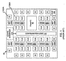
- FIG. 1 is a block diagram of a convention FPGA 90, which includes input/output (I/O) blocks 102A (each labelled 10) located around the perimeter of the FPGA, multi-gigabit transceivers (MGT) 104A interspersed with the I/O blocks, configurable logic blocks 106A (each labelled CLB) arranged in an array, block random access memory 108A (each labelled BRAM) interspersed with the CLBs, configuration logic 112, configuration interface 114, on-chip processor 92 (labelled PowerPC®) and internal configuration access port (ICAP) 120.
- FIG. 1 shows a relatively small number of I/O blocks, CLBs and block RAMs for illustration purposes. It is understood that an FPGA typically includes many more of these elements.
- On-chip processor 92 is an IBM PowerPC® 405 processor.
- FPGA 90 can include more than one of these processors (typically up to for of these processors).
- FPGA 90 also includes other elements, such as a programmable interconnect structure and a configuration memory array, which are not illustrated in FIG. 1 .
- FPGA 90 is described in more detail in " virtex-IITM Pro, Platform FPGA Handbook", (October 14, 2002 ) which includes " Virtex-II ProTM Platform FPGA Documentation” (March 2002 ) "Advance Product Specification,” “Rocket I/O Transceiver User Guide”, “PPC 405 User Manual” and “PPC 405 Processor Block Manual” available from Xilinx, Inc., 2100 Logic Drive, San Jose, CA 95124.
- FPGA 90 is configured in response to a set of configuration data values, which are loaded into a configuration memory array of FPGA 90 (not shown) from an external memory, e.g., a read-only memory (ROM), via configuration interface 114 and configuration logic 112.
- Configuration interface 114 can be, for example, a select map interface, a JTAG interface, or a master serial interface.
- the configuration memory array can be visualized as a rectangular array of bits. The bits are grouped into frames that are one-bit wide words that extend from the top of the array to the bottom.
- the configuration data values are loaded into the configuration memory array one frame at a time from the external memory via the configuration interface 114.
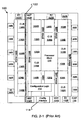
- Figs. 2-1 and 2-2 are simplified conceptual diagrams of the configuration memory array.
- the bits of the configuration memory array 100 (and 101) configure, for example, the CLBs 106B, BRAMs 108B, MGTs 104B, and I/Os 102B.
- the labels are chosen so that the configuration memory array elements (with a B suffix) in Figs. 2-1 and 2-2 correspond to their associated physical components (with an A suffix) in FIG. 1 .
- a frame 122 is a column one bit wide extending from the top of the array 100 to the bottom.
- a frame is the smallest part of the configuration memory array that can be written to or read from.
- the processor block is either a hard-core processor, e.g., processor block 110 of FIG. 2-1 and processor 92 of FIG. 1 , such as the PowerPC® of IBM Corp. of Armonk, NY, or a soft core processor having CLBs, e.g., processor block 109 of FIG. 2-2 , such as the MicroBlaze TM processor core of Xilinx Inc. of San Jose, CA.
- the internal configuration access port (ICAP) 120 was added.
- the ICAP 120 gives access by the FPGA's internal logic (e.g., CLB's 106A and BRAMs 108A) to the configuration memory array 100 (and 101).
- the FPGA's internal logic e.g., CLB's 106A and BRAMs 108A
- the configuration memory array 100 and 101.
- one part of the configured FPGA can reconfigure another part of the FPGA.
- this self-reconfiguration was done by loading pre-generated reconfiguration frames in the BRAM, and using customized logic, over-writing pre-targeted frames in the configuration memory array with these pre-generated reconfiguration frames.
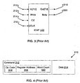
- FIG. 3 shows the ICAP module 120 of the prior art.
- Additional inputs include a chip enable signal 214 and a clock signal 216.
- the busy (done) output signal 220 indicates when data can be received by the ICAP module 120.
- FIG. 4 is a simplified format of a data packet 310 sent to the input bus 210 of the ICAP module 120 of FIG. 3 .
- the data packet 310 includes a command portion 312 having an operation (op) code 316, a register address 318, and a word count 320 for the data portion 314, and the data portion 314.
- the operation code 316 includes commands to the configuration logic 112 to, for example, read from or write to the configuration memory array 100.
- registers in the configuration logic 112 which are identified by register address 318. Further details can be found in Xilinx, Inc. application note, XAPP151, September 27, 2000, titled "Virtex Series Configuration Architecture User Guide.”
- the approach lacks flexibility, as what is to be reconfigured must be predetermined, i.e. the frames pre-generated and the custom logic set.
- any changes to the reconfiguration take a significant amount of time, as the modified reconfiguration must be pre-loaded.
- pre-loading entire frames, when only parts of the frames need to be reconfigured is inefficient.
- more complex dynamic reconfiguration scenarios such as modifying selected resources, generating parameterized circuits on the fly, relocating partial bit streams to other locations on the array are very difficult to implement in custom logic.
- a system is described in US6,204,687 which, in one example, includes a field programmable gate array (FPGA) and an embedded microprocessor.
- FPGA field programmable gate array
- a configuration circuit of the FPGA enables selected memory cells of a frame to be written while a logic plane of the FPGA is operating a user's system.
- the microprocessor communicates with the configuration circuit through one or more dual purpose input/output blocks (IOBs).
- the FPGA includes configuration logic blocks, input/output blocks and interconnect resources whose operations in the logic plane are controlled by user defined configuration data stored in a memory array.
- the memory array includes an input circuit, a shift register, an optional multiplexing circuit and a shadow register. Data bits stored in a frame of the memory array are read into the shadow register. The contents of the shadow register are modified to store new data bits from a shift register under control of a frame mask register. Finally, the contents of the shadow register are transferred back into the memory cells of the frame of the memory array.
- the present invention relates to the self-reconfiguration of an IC, having a plurality of programmable modules, using on-chip processing to perform a read-modify-write of the configuration information stored in the configuration memory array.
- an exemplary embodiment of the present invention provides a method of partially reconfiguring an IC having programmable modules, that includes the steps of (1) loading a base set of configuration information into a configuration memory array for the programmable modules, thereby configuring the IC; (2) reading a frame of configuration information from the configuration memory array; (3) modifying at least part of the configuration information, thereby creating a modified frame of configuration information; and (4) overwriting the existing frame of configuration information in the configuration memory array with the modified frame, thereby partially reconfiguring the IC.
- the steps of reading, modifying and writing are performed under the control of a processor located on the IC.
- An embodiment of the present invention includes a method fro reconfiguring an integrated circuit, having a plurality of programmable logic modules, a processor, a memory array having configuration information for the plurality of programmable logic modules, and a memory module.
- the method includes the steps of: first, reading a section of the configuration information from the memory array. Next, the section is stored in the memory module. The processor then modifies at least some of the section. And lastly, the modified section of the configuration information is written back to the memory array.
- Another embodiment of the present invention includes a method for reconfiguring a programmable logic device, where the programmable logic device has a plurality of programmable components, a configuration memory array, a processor, and a plurality of block memory modules.
- the method includes the steps of: first, reading configuration data for a programmable component from the configuration memory array. Next, the configuration data is stored in a block memory. The processor then partially modifies the stored configuration data. And lastly, and the partially modified configuration data is written back to the configuration memory array.
- a further embodiment of the present invention includes an integrated circuit having programmable logic components.
- the IC further includes: a first memory storing configuration information for the programmable logic components; an access port having access to the first memory; a processor connected by a first bus to a second memory; and a control module connected to the access port and the first bus, where the control module receives control information from the processor via the first bus, and the control information configures the control module to transfer part of the configuration information to the second memory from the first memory via the access port.
- Another embodiment of the present invention includes a programmable logic device having: a processor, a memory, a configuration memory array for configuring the programmable logic device, an access port having access to the configuration memory array, and a control module for controlling the access port.
- the control module includes: an address module configured to determine one or more addresses in the memory for storing data from the configuration memory array, where the address module receives a start address from the processor; and a status register connected to the processor and having a flag indicating to the processor an end of a transfer cycle.
- An aspect of the present invention includes a graphical user interface (GUI) for reconfiguring bits of a configuration memory array of a programmable logic device.
- GUI graphical user interface
- the GUI includes: a window displaying at least part of the configuration memory array; a first region in the window having a first set of bits of the configuration memory array; a memory configured to store a copy of the first set, when a user selects a control to copy the first region; and a second region in the window having a second set of bits of the configuration memory array, said second set over-written by the copy of the first set in response to a command by the user.
- Another aspect of the present invention includes an application programming interface having computer routines stored in a computer readable medium for controlling transfer of a frame between a configuration memory array and a random access memory (RAM) of a programmable logic device, where the computer routines are executed by an processor of the programmable logic device.
- the computer routines include: a first routine for reading the frame from the configuration memory array to the RAM; and a second routine for writing the frame from the RAM to the configuration memory array.
- the IC further includes: a configuration memory array for storing configuration information for the programmable logic components; an access port having access to the configuration memory array; a first processor connected by a first bus to a memory; a second processor connected by the first bus to the memory; a semaphore module having a semaphore, wherein only one processor of the first or second processor is granted the semaphore until a predetermined event occurs; and a control module connected to the access port and the first bus, where the control module receives control information from the one processor granted the semaphore, and where the control information configures the control module to transfer part of the configuration information to the memory from the configuration memory array via the access port.
- Another exemplary embodiment of the present invention provides a method of partially reconfiguring a programmable logic device that includes the steps of (1) loading a base set of configuration data values into a configuration memory array of the programmable logic device, thereby configuring the programmable logic device; (2) reading a first frame of configuration data values from the configuration memory array; (3) modifying a subset of the configuration data values in the first frame of configuration data values, thereby creating a first modified frame of configuration data values; and (4) overwriting the first frame of configuration data values in the configuration memory array with the first modified frame of configuration data values, thereby partially reconfiguring the programmable logic device.
- the steps of reading, modifying and overwriting are performed under the control of a processor located on the programmable logic device.
- the modified subset of configuration data values in the first modified frame are used to control the configuration of multi-gigabit transceivers of the programmable logic device.
- the first modified frame of configuration data values can be used to adjust the pre-emphasis and/or differential voltage characteristics of the multi-gigabit transceivers.
- the subset of the configuration data values in the first frame can be modified in response to a control signal generated external to the programmable logic device.
- the control signal may identify the location of the programmable logic device on a serial back plane.
- the control signal may be provided by a user performing diagnostic tests on the multi-gigabit transceivers.
- the processor can store a plurality of different subsets of configuration data values, wherein each of the subsets represents a different partial reconfiguration of the programmable logic device.
- each of the subsets represents a different partial reconfiguration of the programmable logic device.
- only the configuration data values being modified need to be stored.
- a programmable logic device includes a configuration memory array having a plurality of frames for storing configuration data values, and a processor configured to implement a partial reconfiguration of the programmable logic device by reading a frame from the configuration memory array, modifying only a select subset of the frame, thereby creating a modified frame, and writing the modified frame back to the configuration memory array.
- the processor controls an internal configuration access port coupled between the processor and the configuration memory array, wherein the internal configuration access port retrieves the frame from the configuration memory array under control of the processor.
- One or more block RAMs can be used as a data-side on-chip memory, which stores the frame and modified frame.
- CLB resources of the programmable logic device can be used to implement a direct memory access (DMA) engine coupled between the data-side on-chip memory and the internal configuration access port.
- CLB resources can also be used to implement a device control register coupled to the DMA engine and the processor, wherein the processor controls the DMA engine via the register.
- DMA direct memory access
- the programmable logic device can be configured to implement a processor local bus coupled to the processor, and control logic coupled between the processor local bus and the internal configuration access port.
- the block RAM can also be coupled to the processor local bus.
- a communications interface coupled to the processor local bus can receive internal or external configuration control stimulus.
- an IC having programmable modules and one or more on-chip processors is configured to implement an efficient partial reconfiguration scheme.
- the reconfiguration is performed on one or more frames of the configuration memory array, which includes configuration information or data for the programmable modules, e.g., the CLBs, BRAMs, IOs and MGTs.
- the term "frame” used herein is any set of one or more bits of configuration information and is not limited to a one-bit vertical column.
- modules used in some embodiments of the present invention are similar to or the same as the modules given in Figs. 1 , 2-1 , 2-2 , and 3 and are given the same labels in order to not obscure the invention.
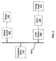
- FIG. 5 is a simplified schematic of a system for self-reconfiguration of an IC of an embodiment of the present invention.
- the IC includes a processor block 110, a BRAM control module 332, a BRAM 108, an ICAP control module 330, and ICAP module 120, and a configuration logic module 112.
- the processor block 110 is coupled to the BRAM control module 332, which controls the BRAM 108.
- the processor block 110 is also coupled to the ICAP control module 330.
- the ICAP control module 330 supplies the data and control signals to and receives the data and busy signal from the ICAP 120 (see FIG. 3 ).
- Embodiments of the present invention show different implementations of the ICAP control module.
- FIG. 6 shows an ICAP control register implementation of an ICAP control module of an aspect of the present invention.
- the ICAP control module 340 has a 32-bit register 325 whose content maps one-to-one with the corresponding data and control signals of the ICAP 120.
- the processor block 110 reads from and writes to register 325 via bus 334.
- the processor block 110 includes the MicroBlazeTM architecture configured using the CLBs 106A, one of the MicroBlazeTM registers is register 325.
- FIG. 7 is a simplified schematic of a system for self-reconfiguration of an IC of a preferred embodiment of the present invention.
- Processor block 110 is connected to a BRAM 338 and ICAP control module 350 via bus 334.
- BRAM 338 includes one or more BRAMs 108A and includes the BRAM control.
- ICAP control module 350 is connected to ICAP 120.
- ICAP 120 is connected to the configuration memory array via the configuration logic 112.
- the configuration memory array includes configuration information or data for the programmable logic components of the IC such as the CLBs.
- Embodiments of the present invention of the ICAP control module 350 are given in FIG. 9 (module 352), FIG. 11 (module 380), and FIG. 16 (module 382).
- the ICAP control module 350 also has a separate dedicated bus 336 to BRAM 338 in order to facilitate data transfer so that the use of the system bus 334 can be reduced or avoided. There is, optionally, a dedicated connection between the processor block 110 and the BRAM 338 (dotted line 333 of FIG. 7 ) or a dedicated connection between the processor block 110 and the ICAP control 350 (dotted line 335 of FIG. 7 ) or both. In an alternative embodiment communications between processor block 110 and BRAM 338 and/or between processor block 110 ICAP control 350 occur directly over these direct links (333, 335) rather than system bus 334.
- FIG. 8 is a block diagram of an architecture using the ICAP of an aspect of the present invention.
- FIG. 8 illustrates a variation of FIG. 7 , where the ICAP control module 352 is an example of ICAP control module 350 of FIG. 7 , and there are two additional buses that provide dedicated connections between the processor block 110 and the BRAM 338 (dotted line 333 of FIG. 7 ) and between the processor block 110 and the ICAP control 350 (dotted line 335 of FIG. 7 ).
- ICAP control module 352 includes a direct memory access (DMA) engine 203 and a device control register (DCR) 204. These elements 203-204 are formed by CLBs, which are configured in response to the base set of configuration data values. As described in more detail below, commands are issued to DMA engine 203 through device control register 204.
- DMA direct memory access
- DCR device control register
- the ICAP control module 352 is connected to ICAP 120.
- Configuration logic 112 is coupled between ICAP 120 and the configuration memory cells, e.g., MGT 104B, CLB 106B, BRAM 108B, and I/O 102B, of the configuration memory array.
- the ports ( FIG. 3 ) of ICAP 120 are accessible to the user logic of FPGA 90 via the general interconnection grid.
- the DSOCM 354 has a direct connection to the ICAP control 350 (ICAP control 352 in FIG. 8 ) via bus 336 and is also connected to processor block 110 via bus 334.
- DSOCM 354 stores, for example, program data, configuration frame data, and bit stream commands for read and write operations.
- An instruction side on-chip memory (ISOCM) 356 (not shown in FIG. 7 ) is also formed by one or more BRAMs 108A and is connected to processor block 110 via bus 334.
- ISOCM 356 stores, for example, instruction code necessary to operate processor block 110.
- ISCOM 356 is merged into DSCOM 354, so that there is only a DSOCM having the contents of both the DSCOM 354 and ISCOM 356.
- FIG. 9 is a block diagram of the contents of device control register 204.
- DCR 204 is a 32-bit register that stores a 4-bit port identification entry (PORT_ID), a 1-bit write enable entry (WR), a 1-bit read-back enable entry (RB), a 1-bit instruction done flag (DONE), a 1-bit reconfiguration done flag (CONFIG_DONE), an 11-bit start address (START_ADDR), an 11-bit end address (END_ADDR), and two unused bits (not shown).
- FIG. 10 is a flow diagram of the operation of the architecture in FIG. 8 , in accordance with one embodiment of the present invention.
- FPGA 90 is powered-up, and a standard configuration is performed by loading a base set of configuration data values in a manner that is known in the art (Step 361).
- the port identification value (PORT_ID) is loaded into the PORT_ID field of device controls register 204.
- Processor 110 reads the PORT_ID from device control register 204 (Step 362).
- processor 110 initiates the partial reconfiguration of the configuration memory array (Step 363). This partial reconfiguration is accomplished as follows (sub-steps 371 to 377).
- processor 110 modifies a read bitstream header in the DSOCM 354 to identify an address of a frame (e.g., Frame_1) of the configuration memory array (Step 371). Then, processor 110 sets the write enable entry (WR) of device control register 204 to a logic "1" value, clears the done flag (DONE) and the reconfiguration done flag (CONFIG_DONE) in device control register 204, and sets the start and end addresses (START_ADDR and END_ADDR) in device control register 204.
- WR write enable entry
- the start address (START_ADDR) is set to identify the address in DSOCM 354 where the read-back bitstream header begins
- the end address (END_ADDR) is set to identify the address in DSOCM 354 where the read bitstream header ends.
- DMA engine 203 Upon detecting the logic "1" write enable entry (WR) in device control register 204, DMA engine 203 routes the read-back bitstream header stored in DSOCM 354 to ICAP 120 (Step 372). DMA engine 203 then sets the DONE flag to a logic "1" state.
- ICAP 120 initiates a configuration frame read operation in response to the received read bitstream header commands. As a result, a frame that includes the configuration data values is retrieved from the configuration memory array, and provided to ICAP 120.
- processor 110 In response to the logic "1" DONE flag, processor 110 resets the write enable entry (WR) to a logic low value, sets the read-back entry (RB) to a logic "1” value, resets the instruction done flag (DONE) to a logic "0" value, and sets the start and end addresses (START_ADDR and END_ADDR) in device control register 204.
- the start address and the end address (START_ADDR and END_ADDR) identify a block in DSOCM 354 where the retrieved frame is to be written.
- DMA engine 203 Upon detesting the logic "1" read-back entry (RB) in device control register 204, DMA engine 203 routes the retrieved frame from ICAP 120 to the location in DSOCM 354 defined by START_ADDR and END_ADDR (Step 373). DMA engine 203 then sets the DONE flag to a logic "1" value.
- processor 110 modifies select configuration bits stored DSOCM 354, by overwriting these configuration bits with new configuration bits. These new configuration bits are selected by processor 110 in response to the PORT_ID value retrieved from device control register 204 (Step 374).
- Processor 110 then resets the DONE flag to a logic "0" value, resets the read-back entry (RB) to a logic “0” value, and sets the write enable entry (WR) to a logic "1" value in device control register 204.
- Processor 110 also sets the start and end addresses (START_ADDR and END_ADDR) in device control register 204.
- the start address (START_ADDR) is set to identify the address DSOCM 354 where the write bitstream header begins, and the end address (END_ADDR) is set to identify the address DSOCM 354 where the write bitstream header ends.
- DMA engine 203 Upon detecting the logic "1" write enable entry (WR) in device control register 204, DMA engine 203 routes the write bitstream header stored in DSOCM 354 to ICAP 120, thereby initiating a write access to the configuration memory array (Step 375). DMA engine 203 then sets the DONE flag to a logic "1" state.
- WR write enable entry
- processor 110 Upon detecting the logic "1" DONE flag, processor 110 resets the DONE flag to a logic “0" state, sets the write enable signal (WR) to a logic "1" value, and sets the start and end addresses (START_ADDR and END_ADDR) in device control register 204.
- the start address (START_ADDR) is set to identify the address in DSOCM 354 where the modified frame begins, and the end address (END_ADDR) is set to identify the address in DSOCM 354 where the modified frame ends.
- DMA engine 203 Upon detecting the logic "1" write enable entry (WR) in DCR 204, DMA engine 203 routes the modified frame stored in DSOCM 354 to ICAP 120.
- ICAP 120 writes the modified frame of configuration data values back to the configuration memory array, such that this modified frame of configuration data values overwrites the previously retrieved frame of configuration data values (Step 376).
- DMA engine 203 sets the DONE flag to a logic "1" value.
- processor 110 Upon detecting the logic "1" DONE flag, processor 110 resets the DONE flag to a logic “0" state, sets the write enable signal (WR) to a logic "1" value, and sets the start and end addresses (START_ADDR and END_ADDR) in DCR 204.
- the start address (START_ADDR) is set to identify the address in DSOCM 354 where the write bitstream trailer begins, and the end address (END_ADDR) is set to identify the address in DSOCM 354 where the write bitstream trailer ends.
- DMA engine 203 Upon detecting the logic "1" write enable entry (WR) in DCR 204, DMA engine 203 transfers the write bitstream trailer stored in DSOCM 354 to ICAP 120, thereby instructing ICAP 120 to complete the write access to the configuration memory array (Step 377). DMA engine 203 then sets the DONE flag to a logic "1" value, and processing returns to Step 363. Sub-steps 371-377 are then repeated until all of the one or more frames storing configuration data values that are to modified, have been read, modified and written in the foregoing manner. At step 364 processor 110 sets the reconfiguration done flag (CONFIG_DONE) in device control register 204 to a logic "1" value, thereby indicating that the one or more frames have been properly reconfigured. FPGA 90 then begins normal operation (Step 365).
- CONFIG_DONE reconfiguration done flag
- FIG. 11 is a schematic of the ICAP control module of a preferred embodiment of the present invention.
- the ICAP control module 380 is an example of the ICAP control module 350 of FIG. 7 .
- the bi-directional data bus 336 in FIG. 7 represents uni-directional data buses 432A and 432B.
- the ICAP control module 380 serves as a pass through for the data buses 432A and 432B, i.e., the ICAP data buses 210 and 218 are directly connected to BRAM data 442 via buses 432A and 432B, respectively.
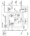
- ICAP control module 380 includes a status register 412, an address control module 420, and a read/write register 410.
- the read/write register 410 is a one bit wide register that is written to by the processor block 110.
- the read/write register 410 When the read/write register 410 is written to it initiates a read/write transfer by asserting the start_transfer signal 534 in FIG. 14 .
- the read/write bit is set to 1 for a read from the ICAP 120 and a 0 for a write to the ICAP 120.
- the read/write register 410 is connected to an inverter 411 which sends the write signal 212 to the ICAP 120 ( FIG. 3 ).
- the status register 412 is a one bit wide register, which when set to 1 by the logic function 414 ((cycle_done 526) AND (NOT (Busy 220))), indicates to the processor block 110 that the read/write transfer for the cycle is complete. After the processor block 110 reads the status register 412, it is reset to 0.
- the address control module 420 includes a BRAM offset register 422, a cycle size register 424, a comparator 425, a cycle counter 426, and an adder 428.
- the address control module 420 generates the memory addresses (BRAM Address 440) for the BRAM data 442 that is being read from and written to by the ICAP 120.
- the memory addresses are sent to BRAM 338 via a bus 430.
- the generation is done by adding via adder 428, the starting or base address given in the BRAM offset register 422 to the current integer count (i.e., index for the array) of the cycle counter 426.
- the cycle counter 426 counts up to the value given in the cycle size register 424 which has the number of (bytes - 1) to be read/write per cycle.
- the comparator 425 compares the current cycle_count 518 from the cycle counter 426 to the cycle_size 520 from the cycle size register 424. Both the BRAM offset register 422 and the cycle_size register 424 can be written to and read from the processor block 110 via bus 334.
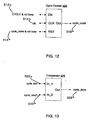
- FIG. 12 shows the control signals for the cycle counter 426 of an aspect of the present invention.
- Cycle counter 426 has input signals including an enable signal EN, a clock signal CLK, and a reset signal RST and an output signal OUT that gives the cycle count, i.e., cycle_count 518.
- the cycle_count 518 is an integer index number that starts at 0 and is incremented by one every clock cycle (c1k 514) until there is a reset.
- the cycle counter 426 is reset (the count is set back to zero), when (cycle_done AND NOT Busy) 512 is asserted, where cycle_done 526 is from the comparator 425 (see FIG. 13 ) and where busy is the Busy signal 220 from the ICAP 120.
- the enable signal receives (CYCLE AND NOT Busy) 512, where CYCLE is 1, when the state machine of FIG. 14 is in the cycle state 532, and where busy is the Busy signal 220 from the ICAP 120.
- the cycle counter 426 hence outputs a new cycle count value when the ICAP Control module 380 is in the cycle state 532 and the ICAP 120 is available (i.e., not busy).
- FIG. 13 shows the input and output signals for the comparator of an aspect of the present invention.
- the comparator 425 receives the cycle size 520 from cycle size register 424 as a first input IN_1, and the cycle_count 518 from the cycle counter 426 ( FIG. 12 ) as a second input In_2.
- the comparator 425 compares the input signal i.e. cycle size minus cycle count, and outputs a one, i.e. cycle_done 526 equals 1, when the difference is 0.
- FIG. 14 shows the finite state machine (FSM) for controlling the reads and writes by the ICAP Control 380.
- the FSM includes an IDLE state 530 in which the cycle counter 426 is in its reset state, and a CYCLE state 532 in which data is transferred between the ICAP 120 and the BRAM 338 starting at the address given by address control module 420.
- the number of bytes transferred in this CYCLE state is cycle_size 520 minus 1.
- the FSM begins in the IDLE state 530 and changes to the CYCLE state 532 when there is a start_transfer signal 534 which is asserted when there is a write to the read/write register 410 by the processor block 110.
- the (cycle_done AND not Busy) signal 414 is asserted, i.e., the transfer of data is complete, the FSM goes back to the IDLE state 530 from the CYCLE state 532.
- FIG. 15 is a flowchart for the ICAP control 380 writing configuration memory array data from the BRAM 338 to the ICAP 120 of an aspect of the present invention.
- processor block 110 sends to the BRAM offset register 422 the starting address in BRAM 388 of the ICAP read instructions to set-up the configuration logic 112 to .send the configuration memory array data for one or more frames.
- ICAP control 380 writes the read instructions in BRAM 338 to ICAP 120 (read/write register 410 is set to zero).
- processor block 110 sets read/write register 410 to one, and ICAP Control 380 transfers the one or more frames from ICAP Output 218 to BRAM data 442 via bus 432B.
- Processor block 110 modifies the one or more frames in BRAM data 442 (step 556).
- the processor block 110 sends to the address control module 420 of ICAP Control 380, the location in BRAM 338 of the write instructions to set-up the configuration logic 112 via ICAP 120 to receive the modified the one or more frames.
- the ICAP Control 380 writes the write instructions in BRAM to ICAP 120 (step 560).
- the ICAP Control 380 continues to write the modified configuration data from BRAM data 442 to ICAP Input 210 via bus 432A (step 562).
- the arrangement of the BRAM 338 was that there was a first area in BRAM 338 where the ICAP read instructions were stored followed by a reserved space where the one or more frames read from the configuration memory array were to be stored. There was a second area for the ICAP write instructions followed by the modified one or more frames to be written back to the configuration memory array. In addition there was a third area in BRAM 338 storing the computer program that the processor block 110 executes.
- the foregoing BRAM memory arrangements were for illustration purposes only, and one of ordinary skill in the arts will recognize that many different storage locations and arrangements are possible.
- ICAP Control 380 As an example implementation for ICAP Control 380 assume that BRAM 338 looks to system bus 334 ( and the processor block 110) as a 512 x 32 bit RAM and to the ICAP Control 380 via buses 430, 432A and 432B, as a 2048 x 8 bit memory. In other words the BRAM 338 is a dual port RAM. Let all data transfers be 32 bits (words). The BRAM offset register 422 and cycle size register 424 are assumed to be 11 bits wide.
- driver routines which are used by the processor block 110 to read and write both control information and data to and from the ICAP Control 380 and the BRAM 338.
- the nine driver routines are as follows:
- the processor block 110 in interfacing with the ICAP control module 380 and BRAM 338 via system bus 334 as configuration data is read from the ICAP 120 to BRAM 338, modified by processor block 110, and written from BRAM 338 to ICAP 120, executes some of the above functions.
- devicewrite() causes the ICAP read instructions to be written from BRAM 338 to the configuration logic 112 (see FIG. 7 ).
- the processor executes a deviceRead() which causes, for example, a frame of configuration memory array information to be transferred from the configuration logic 112 to BRAM 338 via ICAP 120, ICAP control 350, and bus 336.
- the processor block 110 retrieves a selected word from the frame from BRAM using a storageBufferRead(), modifies the word and writes it back to the BRAM 338 when a storageBufferWrite() is executed.
- the processor repeats the above process in order to modify some or all the words in the frame.
- a deviceWrite() transfers the ICAP write instructions followed by the modified frame data from BRAM 338 to the configuration logic 112 via bus 336.
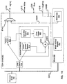
- FIG. 16 is a schematic of the ICAP control module of an alternative embodiment of the present invention.
- the ICAP control module 382 is another example of the ICAP control module 350 of FIG. 7 .
- the bi-directional data bus 336 in FIG. 7 represents uni-directional data buses 632A and 632B in FIG. 16 .
- the ICAP control module 330 serves as a pass through for the data buses 432A and 432B, i.e., the ICAP data bus 210 is connected to BRAM 338 via bus 632A and multiplexer 614 and the ICAP data bus 218 is directly connected to BRAM 338 via bus 632B.
- ICAP control module 382 includes a On-chip Peripheral Bus (OPB) Controller 610, a packet register 612, an address control module 616, and a multiplexer 614.
- the processor block 110 sends an ICAP data packet 310 ( FIG. 3 ) to packet register 612.
- the processor block 110 also sends the starting address in BRAM 338 to read/write the data from/to the ICAP 120.
- the OPB controller 610 insures the information from the processor block 110 goes to the right register (packet register 612 or BRAM address register 618).
- the address control module 616 includes a BRAM address register 618, a cycle size register 620, a cycle counter 622, and an adder 624.
- the address control module 616 generates the memory addresses (BRAM Address 640) for the BRAM data 642 that is being read from and written to by the ICAP 120.
- the memory addresses are sent to BRAM 338 via a bus 626.
- the generation is done by adding via adder 624, the starting or base address given in the BRAM address register 618 to the current integer count (i.e., index for the array) of the cycle counter 622.
- the cycle counter 622 counts up to the value given in the cycle size register 620 which has the number of (bytes - 1) to be read/write per cycle.
- the cycle size register 620 gets the total count from the word count 320 in ICAP data packet 310 ( FIG. 3 ) stored in packet register 612.
- FIG. 17 is a layered architecture of an aspect of the present invention.
- the layered approach is used so that an element at one layer or level can be changed without affecting the other levels.
- levels 0 and 1 are hardware dependent and levels 2, 3 and 4 are hardware independent.
- ICAP controller For an processor such as,processor block 110, embodiments of the ICAP controller have been given in Figs. 6 , 8 , 11 , and 16 .
- Examples of device drivers 712 include setCycleSizeReg(), getStorageBufferSizeReg(), setOffsetReg() getOffsetReg(), setBaseAddr(), getStatusReg(), and setDirectionReg().
- Level 2 has an Application Program Interface (API) 730, which has routines given in Table 1 below.
- API Application Program Interface
- Table 1 Routines Description storageBufferWrite() Writes data to the BRAM 338 storageBufferRead() Reads data from BRAM 338 devicewrite() Writes specified number of bytes from BRAM 338 to ICAP 120 deviceRead() Reads specified number of bytes from ICAP 120 to BRAM 338 deviceAbort() Aborts the current operation deviceReadFrame() Reads one frame from ICAP 120 into the BRAM 338 deviceReadFrames() Reads multiple frames from ICAP 120 into the BRAM 338 devicewriteFrame() Writes one frame to ICAP 120 from the BRAM 338 deviceWriteFrames() Writes multiple frames to ICAP 120 from the BRAM 338 setConfiguration() Loads a configuration from a specified memory location getConfiguration() Writes current configuration to a specified memory
- the routines in API 730 are also layered and the layers for Table 1 are given in Table 2 below.
- the layered approach allows the replacement of lower layers with faster hardware implementations without making changes to the higher layers.
- Table 2 Layers Routines in Layer Layer 0 storageBufferWrite(), storageBufferRead(), deviceWrite(), deviceRead(), deviceAbort() Layer 1 deviceReadFrame(), deviceWriteFrame() Layer 2 deviceReadFrames(), deviceWriteFrames() Layer 3 setConfiguration(), getConfiguration()
- a toolkit 732 providing routines to the application 734 for dynamic resource modification, i.e., resource modification on the fly, including relocatable modules.
- routines in Table 2 above these routine may be readily incorporated by a user in application programs written in high level languages such as C, C++, C#, VB/VBA, and the like. Examples of such level 3 routines are given in Table 3 below.
- the toolkit 732 provides two functions for dealing with relocatable modules:
- the setModule() function moves the bits in a region of the configuration memory array from one location to another.
- the setModule() works on a partial bitstream that contains information about all of the rows in the included frames. It works by modifying the register address 318 ( FIG. 4 ) located in the command portion 312 of the configuration data packet 310.
- FIG. 18 shows an example of a module being moved from an old location 812-1 to a new location 812-2 on the configuration memory array ( Figs. 2-1 and 2-2 ) by the setModule() function.
- the module has N frames located at location 812-1 with a corner point of fromY1 814, where N is a positive number. These N frames are then relocated to location 812-2 with corner point toY1 816.
- the copyModule() function copies any sized rectangular region of the configuration memory array and writes it to another location.
- the copied region contains just a subset of the rows in a frame. This allows the creation of dynamic regions that have static regions above and/or below it.
- the copyModule() function employs a read/modify/write strategy like the resource modification functions. This technique works well for changing select bits in a frame and leaving the others bits in their current configured state.
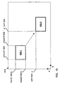
- FIG. 19 shows an example of a module being copied from an old location 820-1 to a new location 820-2 on the configuration memory array ( Figs. 2-1 and 2-2 ) by the copyModule() function.
- the rectangular region 820-1 has y-coordinates fromY1 830 and fromY2 832, which show the location of the original N frames.
- the X coordinates fromX1 840 and fromX2 842 are the locations of the rows in the original N frames.
- the top corner coordinate used as a reference for the copied region 820-1 is (toX1 844, toY1 834).
- the setCLBBits() is a more generalized function than the setLUT() function.
- the setCLBBits () can be used to set the value of a LUT instead of setLUT().
- the setCLBBits () is not as efficient as setLUT(). This is because setLUT() knows that all the bits that control the LUT are located in one frame, so that setLUT() can read one frame, modify the M bits (where M is a predetermined integer value), and then writes back the modified frame.
- setCLBBits () does a read/modify/write M times, as there is no assumed predetermined location for the frame each bit is in.
- GUI graphical user interface
- the interface to the configuration memory array is via the ICAP control module and the ICAP 120. If there is an external processor then access to the configuration memory array is via the configuration interface 114, such as the select map interface.
- the layered architecture of FIG. 17 allows the API 730 and toolkit 732 to be hardware independent.
- the Application layer 734 is written in a high level language such as C or C++.
- FIGs. 1 , 2-1 , and 2-2 only show one processor in order not to obscure the invention.
- the Virtex II Pro TM of Xilinx Inc. of San Jose, CA has upto four PowerPC®s.
- embodiments of the present invention are not limited to one processor, but include one or more processors.
- an arbitration mechanism such as a semaphore, is needed to control access to the shared resource, so that only one processor accesses the shared resource at a time.
- the ICAP 120 is a shared resource to the multiple processors.
- a semaphore is used to control access to the ICAP.
- FIG. 20 is a block diagram of a multiprocessor system using a semaphore to control access to a shared resource of an embodiment of the present invention.
- FIG. 20 has some blocks similar to those in FIG. 7 and those blocks are labeled with the same number.
- FIG. 20 shows two processors, i.e., processor blocks 910 and 110, that are connected via a system bus 334 to BRAM 338, semaphore module 920, and ICAP control 350.
- the BRAM 338 and ICAP control 350 are shared resources to the multiple processors.
- a processor block e.g., 110
- the processor 110 will poll until access is granted.
- processor block 110 can access ICAP control 350 and read, write, or modify one or more frames from the configuration memory array.
- Processor 110 is responsible for releasing the semaphore.
- the watchdog timer 930 counts down to zero from a predefined value.
- the watchdog timer 930 is reset to the predefined value.
- processor block 110 must request the semaphore again from semaphore module 920 before processor block 110 can have access to ICAP control 350.
- FIG. 21 shows the events vs. time for two processor blocks trying to use a shared resource, for example, BRAM 338 or ICAP control 350 of an aspect of the present invention.
- Processor block 110 at time t1 sends request 940 to semaphore module 920 and receives a grant 942 of the semaphore.
- processor block 110 then reads 944 one or more frames from the configuration memory array via ICAP control 350, modifies 946 one or more of the frames, and writes 948 the one or more modified frames back to the configuration memory array via ICAP control 350.
- Processor block 110 then frees 950 the semaphore in semaphore module 920.
- processor block 910 requests 952 from semaphore module 920 the semaphore for access to ICAP control 350. As the semaphore has been granted to processor block 110, the request 952 by processor block 910 is denied 954. Processor block 910 polls semaphore module 920 (request 956, deny 958) until the semaphore is free 950. At time t3 processor block 910 in response to its request 960 for the semaphore is then granted 962 by semaphore module 920. While the examples given above for the shared resource were the BRAM 338 and ICAP control 350, the use of the semaphore as described can be applied to any shared resource.
- a programmable logic device having an on-chip processor is configured to implement an efficient partial reconfiguration scheme.
- a conventional Virtex-II TM Pro FPGA available from Xilinx, Inc., is used to implement the partial reconfiguration scheme.
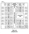
- FPGA 1100 Fig. 22
- some embodiments of the present invention are described in connection with the partial reconfiguration of FPGAs, it is understood that the partial reconfiguration scheme of the present invention may also be implemented using other programmable logic devices.
- the partial reconfiguration scheme is described in connection with the partial reconfiguration of the multi-gigabit transceivers (MGTs) 1111-1114 of FPGA 1100. However, it is understood that other elements of FPGA 1100 can be partially reconfigured in accordance with the principles described below.
- MGTs 1111-1114 are reconfigured in order to optimize the operation of these transceivers.
- MGTs 1111-1114 transmit differential signals to another chip at rates up to 3.125 Gigabits per second (Gbps).
- Gbps Gigabits per second
- the length of the traces used to transmit these differential signals can vary, depending on the physical locations of the FPGA and the receiving chip.
- FPGA 1100 may be located on a printed circuit board that is plugged into a slot of a serial back plane. In this case, the length of the traces between FPGA 1100 and the receiving chip is determined by the particular slot into which the FPGA has been inserted.
- MGTs 1111-1114 can be configured to provide different levels of pre-emphasis to the transmitted differential signals.
- two configuration memory cells in each MGT are used to select one of four levels of signal pre-emphasis. More specifically, two "pre-emphasis" configuration memory cells in each MGT can be set to have a value of "00" in order to provide 10 percent pre-emphasis to the differential transmit signals. Similarly, these two pre-emphasis configuration memory cells can be set to have values of "01", "10” or "11” to provide 20 percent, 25 percent or 33 percent pre-emphasis, respectively, to the differential transmit signals.
- MGTs 1111-1114 can also be configured to provide different differential output voltages.
- three configuration memory cells in each MGT are used to select one of five differential output voltages. More specifically, three "differential output voltage" configuration memory cells in each MGT can be set to have a value of "001" in order to provide an output signal having a differential voltage of 400 mV. Similarly, these three differential output voltage configuration memory cells can be set to have values of "010", “011", “100” or “101” to provide output signals having differential voltages of 500 mV, 600 mV, 700 mV or 800 mV, respectively.
- the pre-emphasis and differential output voltage configuration memory cells for each MGT are located in the same frame of the configuration memory array.
- the pre-emphasis and differential output voltage configuration memory cells for MGTs 1111, 1112, 1113 and 1114 are located in four corresponding frames Frame_1, Frame_2, Frame_3 and Frame_4 of the configuration memory array.
- FPGA 1100 is initially configured in response to a base set of configuration data values, which are provided by an external memory.
- this base set of configuration data values configures MGTs 1111-1114 in a predetermined base configuration.
- the pre-emphasis configuration memory cells may be loaded with a value of "00”
- the differential output voltage configuration memory cells may be loaded with a value of "001”.
- a port identification signal (PORT_ID), which is a static 4-bit code provided on pins of FPGA 1100, identifies the location of the FPGA in the serial back plane. Thus, the port identification signal is representative of the length of the transmission channel between the FPGA and a receiving chip.
- the port identification signal is provided to processor 1103 on FPGA 1100.
- Processor 1103 is programmed to store different sets of pre-emphasis and differential output voltage configuration data values, wherein each set corresponds with a different port identification signal.
- processor 1103 accesses a corresponding set of pre-emphasis and differential output voltage configuration data values.
- Processor 1103 also causes a frame of configuration data values, which includes the pre-emphasis and differential output voltage configuration data values for one of MGTs 1111-1114, to be read from the configuration memory array. Processor 1103 then modifies the retrieved frame of configuration data valuers by overwriting the original pre-emphasis and differential output voltage configuration data values with the set of pre-emphasis and differential voltage configuration data values associated with the port identification signal. Processor 1103 then causes the modified frame of configuration data values to be written back to the configuration memory array, thereby modifying the properties of the associated MGT. The above-described read-modify-write process is then repeated for the other MGTs on FPGA 1100.
- the MGTs can also be tuned for other reasons, including characterization, changing system environments and diagnostics.
- FPGA 1100 is used to implement the read-modify-write process for partially reconfiguring the MGTs.
- Fig. 23 is a block diagram of an internal configuration access port (ICAP) control module 1200 in accordance with one embodiment of the present invention.
- ICAP control module 1200 enables MGTs 1111-1114 to be reconfigured using a read-modify-write scheme.
- MGTs 1111-1114 includes a corresponding set of 5 configuration memory cells 1211-1214, which control the pre-emphasis and differential output voltage settings of the MGT.
- ICAP control module 1200 is configured using various elements of FPGA 1100 ( Fig. 22 ).
- ICAP control module 1200 includes processor 1103 and internal configuration access port 1104.
- Internal configuration access port 1104 which is a hardwired module found in every Virtex-IITM and Virtex-IITM Pro FPGA, has an interface similar to communications interface 1102 ( Fig. 22 ).
- Configuration logic 1101 is coupled between ICAP 1104 and the configuration memory cells 1211-1214 of the configuration memory array.
- the ports of internal configuration access port 1104 are accessible to the user logic of FPGA 1100 via the general interconnect.
- ICAP control module 1200 also includes a data side on-chip memory (DSOCM) 1201, which is formed by a block RAM 1121, and an instruction side on-chip memory (ISOCM) 1202, which is formed by two block RAMs 1122-1123.
- DOCM data side on-chip memory
- ISOCM instruction side on-chip memory
- data-side OCM 1201 is used to store program data, configuration frame data, and bit stream commands for read-back and write operations.
- Instruction-side OCM 1202 stores instruction code necessary to operate processor 1103.
- ICAP control module 1200 also includes a direct memory access (DMA) engine 1203 and a device control register (DCR) 1204. These elements 1203-1204 are formed by CLBs, which are configured in response to the base set of configuration data values. As described in more detail below, commands are issued to DMA engine 1203 through device control register 1204. DMA engine 1203 and device control register 1204 use 2 percent or less of the programmable logic of FPGA 1100.
- DMA direct memory access
- DCR device control register
- ICAP control module 1200 Because only three block RAMs are used to implement ICAP control module 1200, this module does not consume excessive block RAM resources of FPGA 1100. Moreover, the only CLB resources consumed by ICAP control module 1200 include those necessary to create DMA engine 1203 and device control register 1204. Thus, ICAP control module 1200 consumes minimal programmable logic resources on FPGA 1100.
- Fig. 24 is a block diagram of device control register 1204.
- Device control register 1204 is a 32-bit register that stores a 4-bit port identification entry (PORT_ID), a 1-bit write enable entry (WR), a 1-bit read-back enable entry (RB), a 1-bit instruction done flag (DONE), a 1-bit reconfiguration done flag (CONFIG_DONE), an 11-bit start address (START_ADDR), an 11-bit end address (END_ADDR), and two unused bits (not shown).
- Fig. 25 is a flow diagram that defines the operation of ICAP control module 1200, in accordance with one embodiment of the present invention. As will become apparent in view of the following disclosure ( Fig. 26 ), this flow diagram is equally applicable to other embodiments of present invention.
- FPGA 1100 is powered-up, and standard configuration is performed by loading a base set of configuration data values in a manner that is known in the art (Step 1401).
- An internal or external stimulus such as the port identification value (PORT_ID) provided on the pins of FPGA 1100, is loaded into the PORT_ID field of device control register 1204.
- Processor 1103 reads the PORT_ID from device control register 1204 (Step 1402).
- processor 1103 initiates the partial reconfiguration of MGTs 1111-1114 (Step 1403). This partial reconfiguration is accomplished as follows.
- processor 1103 modifies a read-back bitstream header in data-side OCM 1201 to identify an address of a frame (e.g., Frame_1) of the configuration memory array that includes the configuration data values for a subset of the MGTs (e.g., MGT 1111) (Step 1411). Then, processor 1103 sets the write enable entry (WR) of device control register 1204 to a logic "1" value, clears the done flag (DONE) and the reconfiguration done flag (CONFIG_DONE) in device control register 1204, and sets the start and end addresses (START_ADDR and END_ADDR) in device control register 1204.
- WR write enable entry
- the start address (START_ADDR) is set to identify the address in data-side OCM 1201 where the read-back bitstream header begins
- the end address (END_ADDR) is set to identify the address in data-side OCM 1201 where the read-back bitstream header ends.
- DMA engine 1203 Upon detecting the logic "1" write enable entry (WR) in device control register 1204, DMA engine 1203 routes the read-back bitstream header stored in data-side OCM 1201 to internal configuration access port 1104 (Step 1412). DMA engine 1203 then sets the DONE flag to a logic "1" state.
- Internal configuration access port 1104 initiates a configuration frame read-back operation in response to the received read-back bitstream header commands. As a result, a frame that includes the configuration data values 1211 is retrieved from the configuration memory array, and provided to internal configuration access port 1104.
- processor 1103 In response to the logic "1" DONE flag, processor 1103 resets the write enable entry (WR) to a logic low value, sets the read-back entry (RB) to a logic "1” value, resets the instruction done flag (DONE) to a logic "0" value, and sets the start and end addresses (START_ADDR and END_ADDR) in device control register 1204.
- the start address and the end address (START_ADDR and END_ADDR) identify a block in data-side OCM 1201 where the retrieved frame is to be written.
- DMA engine 1203 Upon detecting the logic "1" read-back entry (RB) in device control register 1204, DMA engine 1203 routes the retrieved frame from internal configuration access port 1104 to the location in data-side OCM 1201 defined by START_ADDR and END_ADDR (Step 1413). DMA engine 1203 then sets the DONE flag to a logic "1" value.
- processor 1103 modifies select configuration bits (e.g., configuration bit set 1211) stored in data-side OCM 1201, by overwriting these configuration bits with new configuration bits. These new configuration bits are selected by processor 1103 in response to the PORT_ID value retrieved from device control register 1204 (Step 1414). As described in more detail below, these new configuration bits can be selected in response to other internal or external configuration control stimulus in other embodiments. These new configuration bits define the new attributes of the associated MGT (e.g., MGT 1111).
- Processor 1103 then resets the DONE flag to a logic "0" value, resets the read-back entry (RB) to a logic “0” value, and sets the write enable entry (WR) to a logic "1" value in device control register 1204.
- Processor 1103 also sets the start and end addresses (START_ADDR and END_ADDR) in device control register 1204.
- the start address (START_ADDR) is set to identify the address in data-side OCM 1201 where the write bitstream header begins, and the end address (END_ADDR) is set to identify the address in data-side OCM 1201 where the write bitstream header ends.
- DMA engine 1203 Upon detecting the logic "1" write enable entry (WR) in device control register 1204, DMA engine 1203 routes the write bitstream header stored in data-side OCM 1201 to internal configuration access port 1104, thereby initiating a write access to the configuration memory array (Step 1415). DMA engine 1203 then sets the DONE flag to a logic "1" state.
- WR write enable entry
- processor 1103 Upon detecting the logic "1" DONE flag, processor 1103 resets the DONE flag to a logic “0" state, sets the write enable signal (WR) to a logic "1" value, and sets the start and end addresses (START_ADDR and END_ADDR) in device control register 1204.
- the start address (START_ADDR) is set to identify the address in data-side OCM 1201 where the modified frame begins, and the end address (END_ADDR) is set to identify the address in data-side OCM 1201 where the modified frame ends.
- DMA engine 1203 Upon detecting the logic "1" write enable entry (WR) in device control register 1204, DMA engine 1203 routes the modified frame stored in data-side OCM 1201 to internal configuration access port 1104.
- internal configuration access port 1104 writes the modified frame of configuration data values back to the configuration memory array, such that this modified frame of configuration data values overwrites the previously retrieved frame of configuration data values (Step 1416).
- the modified configuration bit set 1211 modifies the configuration of MGT 1111.
- DMA engine 1203 then sets the DONE flag to a logic "1" value.
- processor 1103 Upon detecting the logic "1" DONE flag, processor 1103 resets the DONE flag to a logic “0" state, sets the write enable signal (WR) to a logic "1" value, and sets the start and end addresses (START_ADDR and END_ADDR) in device control register 1204.
- the start address (START_ADDR) is set to identify the address in data-side OCM 1201 where the write bitstream trailer begins, and the end address (END_ADDR) is set to identify the address in data-side OCM 1201 where the write bitstream trailer ends.
- DMA engine 1203 Upon detecting the logic "1" write enable entry (WR) in device control register 1204, DMA engine 1203 transfers the write bitstream trailer stored in data-side OCM 1201 to internal configuration access port 1104, thereby instructing internal configuration access port 1104 to complete the write access to the configuration memory array (Step 1417). DMA engine 1203 then sets the DONE flag to a logic "1" value, and processing returns to Step 1411. Steps 1411-1417 are then repeated until all of the frames storing configuration data values for the MGTs have been read, modified and written in the foregoing manner. In the described example, all of the configuration bit sets 1211-1214 will be modified after the four cycles through Steps 1411-1417. At this time, processor 1103 writes the output results and sets the appropriate flags.
- WR write enable entry
- Step 1404 processor 1103 sets the reconfiguration done flag (CONFIG_DONE) in device control register 1204 to a logic "1" value, thereby indicating that all of the MGTs have been properly reconfigured.
- FPGA 1100 begins normal operation (Step 1405).
- the above-described embodiment only requires that five configuration bits be stored in data-side OCM 1201 for each possible port identification value (PORT_ID). This greatly reduces the required storage capacity for the partial reconfiguration operation, when compared with the prior art schemes. Moreover, the above-described embodiment does not consume excessive logic resources of the FPGA 1100, but rather uses the existing internal configuration access port 1104 and processor 1103. Finally, the above-described embodiment provides a scheme that can be easily implemented by users with little or no processor/programming experience. Another embodiment, described below, may be desired by users having processor/programming expertise.
- Fig. 26 is a block diagram of FPGA 1100, configured in accordance with another embodiment of the present invention.
- FPGA 1100 is configured to implement a processor local bus (PLB) 1501, which is coupled to processor 1103. Access to PLB 1501 is controlled by a dedicated PLB arbiter 1502, which is coupled to processor 1103.
- IPIF block 1511 is used to couple synchronous dynamic random access memory (SDRAM) controller 1521 to PLB 1501.
- SDRAM controller 1521 which is implemented by configuring CLBs on FPGA 1100, is coupled to an external SDRAM 1531.
- external SDRAM 1531 can be used to store header, trailer and reconfiguration data in the same manner as block RAM 1125.
- IPIF block 1512 is used to couple communications interface 1522 to PLB 1501.
- Communications interface 1522 which is implemented by CLBs in the described embodiment, is coupled to receive an internal or external stimulus 1532.
- internal/external stimulus 1532 is used to provide information indicating the manner in which MGTs 1111-1114 are to be configured.
- IPIF block 1513 is used to couple ICAP controller 1523 to PLB 1501. ICAP controller 1523, which is implemented by CLBs in the described embodiment, is coupled to ICAP 1104. ICAP 1104 is coupled to configuration logic 1101, which in turn, is coupled to the configuration memory array. IPIF block 1514 is used to couple bit error rate tester (BERT) 1524 to PLB 1501. BERT 1524 is coupled to MGTs 1113 and 1114 in accordance with one variation of the present invention. In this embodiment, MGT 1113 transmits a predetermined set of signals to MGT 1114 via a communications channel 1534. Similarly, MGT 1114 transmits a predetermined set of signals to MGT 1113 via communications channel 1534.
- BERT bit error rate tester
- Block RAM controller 1525 which is implemented by CLBs in the described embodiment, is coupled to block RAM 1125.
- FPGA 1100 of Fig. 26 can be operated as follows. FPGA 1100 is initially configured in response to a base set of configuration data values, which are provided by an external memory (not shown). This configuration implements PLB 1501 and the associated logic illustrated in Fig. 26 . In addition to configuring the rest of FPGA 1100, this base set of configuration data values configures MGTs 1111-1114 in a predetermined base configuration.
- MGTs 1111-1114 can be reconfigured as follows.
- Internal/external stimulus 1532 provides a reconfiguration instruction/value to communication interface 1522.
- the internal/external stimulus 1532 can be a port identification value (PORT_ID) provided on pins of FPGA 1100, in the manner described above in connection with Fig. 23 .
- Internal/external stimulus 1532 can be implemented by external devices, such as a terminal program, a network connection, a host shell, or switches. Alternatively, internal/external stimulus 1532 can be implemented by internal devices, such as processor controlled sequential events, or decision and control based upon a response to an on-chip event or test.
- Communication interface 1522 which receives the reconfiguration instruction/value, can be, for example, a universal asynchronous receiver/transmitter (UART).
- UART universal asynchronous receiver/transmitter
- Communication interface 1522 routes the reconfiguration instruction to IPIF 1512. Under the control of PLB arbiter 1502, IPIF 1512 routes the reconfiguration instruction to processor 1103 via PLB 1501. In response to the reconfiguration instruction provided by internal/external stimulus 1532, processor 1103 initiates the partial reconfiguration of MGTs 1111-1114. This partial reconfiguration is accomplished as follows.
- processor 1103 modifies a read-back bitstream header, which is stored in either external SDRAM 1531 or block RAM 1125, to identify an address of a frame (e.g., Frame_1) in the configuration memory array that includes the configuration data values for one of MGTs 1111-1114 (e.g., MGT 1111).
- Processor 1103 accesses SDRAM 1531 (or block RAM 1125) via PLB 1501.
- Processor 1103 then causes the read-back bitstream header stored in SDRAM 1531 or block RAM 1125 to be retrieved and routed to internal configuration access port 1104 (via PLB 1501).
- Internal configuration access port 1104 initiates a configuration frame read-back operation in response to the received read-back bitstream header commands.
- the frame (Frame_1) that includes the configuration data values 1211 of MGT 1111 is retrieved from the configuration memory array, and provided to internal configuration access port 1104.
- Processor 1103 routes the retrieved frame from internal configuration access port 1104 to external SDRAM 1531 or block RAM 1125 (via PLB 1501). Processor 1103 then modifies select configuration bits (e.g., configuration bit set 1211) stored in external SDRAM 1531 or block RAM 1125, by overwriting these configuration bits with new configuration bits. These new configuration bits are selected by processor 1103 in response to the reconfiguration instruction received from internal/external stimulus 1532. These new configuration bits define the new attributes of the associated MGT 1111.
- select configuration bits e.g., configuration bit set 1211
- Processor 1103 then routes a write bitstream header stored in external SDRAM 1531 or block RAM 1125 to internal configuration access port 1104 (via PLB 1501), thereby initiating a write access to the configuration memory array.
- Processor 1103 then routes the modified frame stored in external SDRAM 1531 or block RAM 1125 to internal configuration access port 1104 (again, via PLB 1501).
- internal configuration access port 1104 writes the modified frame of configuration data values back to the configuration memory array, such that this modified frame of configuration data values overwrites the previously retrieved frame of configuration data values.
- the modified configuration bit set 1211 modifies the configuration of MGT 1111.
- Processor 1103 then transfers a write bitstream trailer stored in external 1531 or block RAM 1125 to internal configuration access port 1104 (via PLB 1501), thereby instructing internal configuration access port 1104 to complete the write access to the configuration memory array. This process is repeated until all of the frames storing configuration data values for the MGTs have been read, modified and written in the foregoing manner. FPGA 1100 can then begin normal operation.
- BERT 1524 can be used to enable adaptive modification of the characteristics of MGTs 1111-1114.
- MGTs 1111-1114 are configured to a predetermined base configuration in the manner described above.
- Processor 1103 then instructs BERT 1524 (via PLB 1501) to run a bit error rate test in the following manner.
- BERT 1524 transmits a first set of predetermined differential signals from the transmit port of MGT 1113 to the receive port of MGT 1114, over a communications channel 1534.
- BERT 1524 transmits a second set of predetermined differential signals (which may be identical to the first set) from the transmit port of MGT 1114 to the receive port of MGT 1113, over communications channel 1534.
- MGTs 1113 and 1114 provide the received signals to BERT 1524, which determines the bit error rate of communications channel 1534.
- Communications channel 1534 is representative of the communications channel to be used by MGTs 1111-1114 during normal operation.
- BERT 1524 reports the determined bit error rate to processor 1103. If this bit error rate is unacceptable, processor 1103 can reconfigure MGTs 1111-1114 in the manner described above, and then re-test the bit error rate. This .process can be repeated until an optimal configuration is determined for MGTs 1111-1114.
- FIG. 25 An adaptive loop, such as the one described above, is illustrated by dashed line 1420 in Fig. 25 .
- This dashed line 1420 indicates that after the partial reconfiguration is completed in Step 1404 or Step 1405, processing may return to Step 1402, where processor 1103 reads the internal/external stimulus (which has been modified in response to the partial reconfiguration), and in response, proceeds with another partial reconfiguration.
- FPGA 1100 can be used to control the partial reconfiguration of another FPGA, which may or may not include an associated processor.
- Fig. 27 is a block diagram illustrating an embodiment in which FPGA 1100 is used to implement partial reconfiguration of another FPGA 1600.
- FPGA 1600 which includes configuration logic 1601 and configuration interface 1602, may or may not include a processor.
- FPGA 1100 is configured in the manner described above in connection with either Fig. 23 or Fig. 26 .
- a communications channel 1650 is provided between FPGA 1100 and FPGA 1600. Communications channel 1650 links either DMA engine 1203 ( Fig. 23 ) or the processor local bus 1501 ( Fig. 26 ) of FPGA 1100 with a configuration interface 1602 of FPGA 1600.
- Configuration interface 1602 is substantially similar to configuration interface 1102 of FPGA 1100. In one embodiment, configuration interface 1602 is substantially identical to internal configuration access port 1104, with the difference being that internal configuration access port 1104 is accessed via user logic, and configuration interface 1602 is accessed via external logic.
- FPGA 1100 operates in the manner described above to read a frame from the configuration memory array of FPGA 1600 (via communications channel 1650, configuration interface 1602 and configuration logic 1601). FPGA 1100 then modifies the frame retrieved from FPGA 1600 by overwriting select configuration bits of the frame in the manner described above. Note that the frame is modified using the resources of FPGA 1100. FPGA 1100 then writes the modified frame back to FPGA 1600 (via communications channel 1650, configuration interface 1602 and configuration logic 1601).
- this embodiment enables the resources of one FPGA (e.g., FPGA 1100) to be used to partially reconfigure one or more other FPGAs (e.g., FPGA 1600).
- the software functionality can be further combined or even separated.
- the hardware functionality can be further combined, or even separated.
- the software functionality can be implemented in terms of hardware or a combination of hardware and software.
- the hardware functionality can be implemented in software or a combination of hardware and software.
Landscapes
- Physics & Mathematics (AREA)
- Engineering & Computer Science (AREA)
- Mathematical Physics (AREA)
- Computer Hardware Design (AREA)
- General Engineering & Computer Science (AREA)
- Computing Systems (AREA)
- Theoretical Computer Science (AREA)
- General Physics & Mathematics (AREA)
- Logic Circuits (AREA)
Description
- The present invention relates to reconfiguration of an Integrated Circuit (IC) having programmable modules. More specifically, the present invention relates to the full or partial self-reconfiguration of the programmable modules.
- Dynamic reconfiguration and self-reconfiguration are two of the more advanced forms of field programmable gate array (FPGA) reconfigurability. Dynamic reconfiguration involves the active FPGA being fully or partially reconfigured, while ensuring the correct operation of those active circuits that are not being changed. Self-reconfiguration extends the concept of dynamic reconfigurability. It assumes that specific circuits on the FPGA itself are used to control the reconfiguration of other parts of the FPGA. Both dynamic reconfiguration and self-configuration rely on an external reconfiguration control interface to boot an FPGA when power is first applied or the device is reset.
-
US 6,204,687 describes a FPGA configuration circuit including a bus interface for applying a bit stream form either a JTAG interface or an input/output block (IOB) interface onto a bus. The bus interface parses a header word from the bit stream into an address field and an operand field. Several registers are connected to the bus. The bus interface generates control signals in response to the address field and the operand field that cause one or more registers to perform predefined operations according to subsequent data words in the bit stream. Partial reconfiguration is performed by storing the addresses of selected frames of the configuration memory array in a frame address register, which addresses selected frames in a configuration memory array. -
FIG. 1 is a block diagram of aconvention FPGA 90, which includes input/output (I/O) blocks 102A (each labelled 10) located around the perimeter of the FPGA, multi-gigabit transceivers (MGT) 104A interspersed with the I/O blocks,configurable logic blocks 106A (each labelled CLB) arranged in an array, blockrandom access memory 108A (each labelled BRAM) interspersed with the CLBs,configuration logic 112,configuration interface 114, on-chip processor 92 (labelled PowerPC®) and internal configuration access port (ICAP) 120. AlthoughFIG. 1 shows a relatively small number of I/O blocks, CLBs and block RAMs for illustration purposes. It is understood that an FPGA typically includes many more of these elements. On-chip processor 92 is an IBM PowerPC® 405 processor.FPGA 90 can include more than one of these processors (typically up to for of these processors).FPGA 90 also includes other elements, such as a programmable interconnect structure and a configuration memory array, which are not illustrated inFIG. 1 .FPGA 90 is described in more detail in "virtex-II™ Pro, Platform FPGA Handbook", (October 14, 2002) which includes "Virtex-II Pro™ Platform FPGA Documentation" (March 2002) "Advance Product Specification," "Rocket I/O Transceiver User Guide", "PPC 405 User Manual" and "PPC 405 Processor Block Manual" available from Xilinx, Inc., 2100 Logic Drive, San Jose, CA 95124. - In general,
FPGA 90 is configured in response to a set of configuration data values, which are loaded into a configuration memory array of FPGA 90 (not shown) from an external memory, e.g., a read-only memory (ROM), viaconfiguration interface 114 andconfiguration logic 112.Configuration interface 114 can be, for example, a select map interface, a JTAG interface, or a master serial interface. The configuration memory array can be visualized as a rectangular array of bits. The bits are grouped into frames that are one-bit wide words that extend from the top of the array to the bottom. The configuration data values are loaded into the configuration memory array one frame at a time from the external memory via theconfiguration interface 114. -
Figs. 2-1 and2-2 are simplified conceptual diagrams of the configuration memory array. The bits of the configuration memory array 100 (and 101) configure, for example, theCLBs 106B,BRAMs 108B,MGTs 104B, and I/Os 102B. InFIGs. 2-1 and2-2 the labels are chosen so that the configuration memory array elements (with a B suffix) inFigs. 2-1 and2-2 correspond to their associated physical components (with an A suffix) inFIG. 1 . Aframe 122 is a column one bit wide extending from the top of thearray 100 to the bottom. A frame is the smallest part of the configuration memory array that can be written to or read from. - The processor block is either a hard-core processor, e.g.,
processor block 110 ofFIG. 2-1 andprocessor 92 ofFIG. 1 , such as the PowerPC® of IBM Corp. of Armonk, NY, or a soft core processor having CLBs, e.g.,processor block 109 ofFIG. 2-2 , such as the MicroBlaze™ processor core of Xilinx Inc. of San Jose, CA. - In order to provide self-reconfiguration for the FPGA, the internal configuration access port (ICAP) 120 was added. The ICAP 120 gives access by the FPGA's internal logic (e.g., CLB's 106A and
BRAMs 108A) to the configuration memory array 100 (and 101). In other words, one part of the configured FPGA can reconfigure another part of the FPGA. Conventionally, this self-reconfiguration was done by loading pre-generated reconfiguration frames in the BRAM, and using customized logic, over-writing pre-targeted frames in the configuration memory array with these pre-generated reconfiguration frames. -
FIG. 3 shows the ICAPmodule 120 of the prior art. There is an eight bitwide input bus 210 and an eight bitwide output bus 218. Theinput write signal 212 indicates when there is a read from or write to the ICAP module 120 (where, e.g., write = 1 and read = 0). Additional inputs include a chip enable signal 214 and a clock signal 216. The busy (done) output signal 220 indicates when data can be received by theICAP module 120. -
FIG. 4 is a simplified format of adata packet 310 sent to theinput bus 210 of the ICAPmodule 120 ofFIG. 3 . Thedata packet 310, includes acommand portion 312 having an operation (op)code 316, aregister address 318, and aword count 320 for thedata portion 314, and thedata portion 314. Theoperation code 316 includes commands to theconfiguration logic 112 to, for example, read from or write to theconfiguration memory array 100. There are registers in theconfiguration logic 112, which are identified byregister address 318. Further details can be found in Xilinx, Inc. application note, XAPP151, September 27, 2000, titled "Virtex Series Configuration Architecture User Guide." - There are several disadvantages with using the above custom logic self-reconfiguration approach. First, for example, the approach lacks flexibility, as what is to be reconfigured must be predetermined, i.e. the frames pre-generated and the custom logic set. Second, any changes to the reconfiguration take a significant amount of time, as the modified reconfiguration must be pre-loaded. Third, pre-loading entire frames, when only parts of the frames need to be reconfigured is inefficient. And fourth, more complex dynamic reconfiguration scenarios, such as modifying selected resources, generating parameterized circuits on the fly, relocating partial bit streams to other locations on the array are very difficult to implement in custom logic.
- Accordingly, it would be desirable to have an improved scheme for implementing the self-reconfiguration of an FPGA, which overcomes the above-described deficiencies.
- A system is described in
US6,204,687 which, in one example, includes a field programmable gate array (FPGA) and an embedded microprocessor. A configuration circuit of the FPGA enables selected memory cells of a frame to be written while a logic plane of the FPGA is operating a user's system. The microprocessor communicates with the configuration circuit through one or more dual purpose input/output blocks (IOBs). The FPGA includes configuration logic blocks, input/output blocks and interconnect resources whose operations in the logic plane are controlled by user defined configuration data stored in a memory array. In one embodiment, the memory array includes an input circuit, a shift register, an optional multiplexing circuit and a shadow register. Data bits stored in a frame of the memory array are read into the shadow register. The contents of the shadow register are modified to store new data bits from a shift register under control of a frame mask register. Finally, the contents of the shadow register are transferred back into the memory cells of the frame of the memory array. - The present invention relates to the self-reconfiguration of an IC, having a plurality of programmable modules, using on-chip processing to perform a read-modify-write of the configuration information stored in the configuration memory array.
- Accordingly, an exemplary embodiment of the present invention provides a method of partially reconfiguring an IC having programmable modules, that includes the steps of (1) loading a base set of configuration information into a configuration memory array for the programmable modules, thereby configuring the IC; (2) reading a frame of configuration information from the configuration memory array; (3) modifying at least part of the configuration information, thereby creating a modified frame of configuration information; and (4) overwriting the existing frame of configuration information in the configuration memory array with the modified frame, thereby partially reconfiguring the IC. The steps of reading, modifying and writing are performed under the control of a processor located on the IC.
- An embodiment of the present invention includes a method fro reconfiguring an integrated circuit, having a plurality of programmable logic modules, a processor, a memory array having configuration information for the plurality of programmable logic modules, and a memory module. The method includes the steps of: first, reading a section of the configuration information from the memory array. Next, the section is stored in the memory module. The processor then modifies at least some of the section. And lastly, the modified section of the configuration information is written back to the memory array.
- Another embodiment of the present invention includes a method for reconfiguring a programmable logic device, where the programmable logic device has a plurality of programmable components, a configuration memory array, a processor, and a plurality of block memory modules. The method includes the steps of: first, reading configuration data for a programmable component from the configuration memory array. Next, the configuration data is stored in a block memory. The processor then partially modifies the stored configuration data. And lastly, and the partially modified configuration data is written back to the configuration memory array.
- A further embodiment of the present invention includes an integrated circuit having programmable logic components. The IC further includes: a first memory storing configuration information for the programmable logic components; an access port having access to the first memory; a processor connected by a first bus to a second memory; and a control module connected to the access port and the first bus, where the control module receives control information from the processor via the first bus, and the control information configures the control module to transfer part of the configuration information to the second memory from the first memory via the access port.
- Another embodiment of the present invention includes a programmable logic device having: a processor, a memory, a configuration memory array for configuring the programmable logic device, an access port having access to the configuration memory array, and a control module for controlling the access port. The control module includes: an address module configured to determine one or more addresses in the memory for storing data from the configuration memory array, where the address module receives a start address from the processor; and a status register connected to the processor and having a flag indicating to the processor an end of a transfer cycle.
- An aspect of the present invention includes a graphical user interface (GUI) for reconfiguring bits of a configuration memory array of a programmable logic device. The GUI includes: a window displaying at least part of the configuration memory array; a first region in the window having a first set of bits of the configuration memory array; a memory configured to store a copy of the first set, when a user selects a control to copy the first region; and a second region in the window having a second set of bits of the configuration memory array, said second set over-written by the copy of the first set in response to a command by the user.
- Another aspect of the present invention includes an application programming interface having computer routines stored in a computer readable medium for controlling transfer of a frame between a configuration memory array and a random access memory (RAM) of a programmable logic device, where the computer routines are executed by an processor of the programmable logic device. The computer routines include: a first routine for reading the frame from the configuration memory array to the RAM; and a second routine for writing the frame from the RAM to the configuration memory array.
- Yet another aspect of the present invention includes an integrated circuit having programmable logic components. The IC further includes: a configuration memory array for storing configuration information for the programmable logic components; an access port having access to the configuration memory array; a first processor connected by a first bus to a memory; a second processor connected by the first bus to the memory; a semaphore module having a semaphore, wherein only one processor of the first or second processor is granted the semaphore until a predetermined event occurs; and a control module connected to the access port and the first bus, where the control module receives control information from the one processor granted the semaphore, and where the control information configures the control module to transfer part of the configuration information to the memory from the configuration memory array via the access port.
- Another exemplary embodiment of the present invention provides a method of partially reconfiguring a programmable logic device that includes the steps of (1) loading a base set of configuration data values into a configuration memory array of the programmable logic device, thereby configuring the programmable logic device; (2) reading a first frame of configuration data values from the configuration memory array; (3) modifying a subset of the configuration data values in the first frame of configuration data values, thereby creating a first modified frame of configuration data values; and (4) overwriting the first frame of configuration data values in the configuration memory array with the first modified frame of configuration data values, thereby partially reconfiguring the programmable logic device. The steps of reading, modifying and overwriting are performed under the control of a processor located on the programmable logic device.
- In one embodiment, the modified subset of configuration data values in the first modified frame are used to control the configuration of multi-gigabit transceivers of the programmable logic device. For example, the first modified frame of configuration data values can be used to adjust the pre-emphasis and/or differential voltage characteristics of the multi-gigabit transceivers.
- The subset of the configuration data values in the first frame can be modified in response to a control signal generated external to the programmable logic device. For example, the control signal may identify the location of the programmable logic device on a serial back plane. Alternately, the control signal may be provided by a user performing diagnostic tests on the multi-gigabit transceivers.
- In a particular embodiment, the processor can store a plurality of different subsets of configuration data values, wherein each of the subsets represents a different partial reconfiguration of the programmable logic device. Advantageously, only the configuration data values being modified need to be stored.
- In accordance with another embodiment, a programmable logic device includes a configuration memory array having a plurality of frames for storing configuration data values, and a processor configured to implement a partial reconfiguration of the programmable logic device by reading a frame from the configuration memory array, modifying only a select subset of the frame, thereby creating a modified frame, and writing the modified frame back to the configuration memory array. In one embodiment, the processor controls an internal configuration access port coupled between the processor and the configuration memory array, wherein the internal configuration access port retrieves the frame from the configuration memory array under control of the processor. One or more block RAMs can be used as a data-side on-chip memory, which stores the frame and modified frame. CLB resources of the programmable logic device can be used to implement a direct memory access (DMA) engine coupled between the data-side on-chip memory and the internal configuration access port. CLB resources can also be used to implement a device control register coupled to the DMA engine and the processor, wherein the processor controls the DMA engine via the register.
- In yet another embodiment, the programmable logic device can be configured to implement a processor local bus coupled to the processor, and control logic coupled between the processor local bus and the internal configuration access port. The block RAM can also be coupled to the processor local bus. A communications interface coupled to the processor local bus can receive internal or external configuration control stimulus.
- The present invention will be more full understood in view of the following description and drawings.
-
-
FIG. 1 is a block diagram of a conventional FPGA;Figs. 2-1 and2-2 are simplified conceptual diagrams of the configuration memory array; -
FIG. 3 shows theICAP module 120 of the prior art; -
FIG. 4 is a simplified format of a data packet sent to the input bus of the ICAP module ofFIG. 3 .; -
FIG. 5 is a simplified schematic of a system for self-reconfiguration of an IC of an embodiment of the present invention; -
FIG. 6 shows an ICAP control register implementation of an ICAP control module of an aspect of the present invention; -
FIG. 7 is a simplified schematic of a system for self-reconfiguration of an IC of a preferred embodiment of the present invention; -
FIG. 8 is a block diagram of an architecture using the ICAP of an aspect of the present invention; -
FIG. 9 is a block diagram of a device control register used in the ICAP control module ofFIG. 8 , in accordance with one aspect of the present invention; -
FIG. 10 is a flow diagram of the operation of the architecture inFIG. 8 , in accordance with one embodiment of the present invention; -
FIG. 11 is a schematic of the ICAP control module of a preferred embodiment of the present invention; -
FIG. 12 shows the control signals for the cycle counter of an aspect of the present invention; -
FIG. 13 shows the input and output signals for the comparator of an aspect of the present invention; . -
FIG. 14 shows the finite state machine (FSM) for controlling the reads and writes by the ICAP Control ; -
FIG. 15 is a flowchart for the ICAP control writing configuration memory array data from the BRAM to the ICAP of an aspect of the present invention; -
FIG. 16 is a schematic of the ICAP control module of an alternative embodiment of the present invention; -
FIG. 17 is a layered architecture of an aspect of the present invention -
FIG. 18 shows an example,of a module being moved from an old location to a new location on the configuration memory array by the setModule() function; -
FIG. 19 shows an example of a module being copied from an old location to a new location on the configuration memory array by the copyModule() function; -
FIG. 20 is a block diagram of a multiprocessor system using a semaphore to control access to a shared resource of an embodiment of the present invention; -
FIG. 21 shows the events vs. time for two processor blocks trying to use a shared resource of an aspect of the present invention; -
Fig. 22 is a block diagram of a conventional FPGA; -
Fig. 23 is a block diagram of an internal configuration access port control module in accordance with one embodiment of the present invention; -
Fig. 24 is a block diagram of a device control register used in the internal configuration access port control module ofFig. 23 , in accordance with one embodiment of the present invention; -
Fig. 25 is a flow diagram that defines the operation of an internal configuration access port control module, in accordance with one embodiment of the present invention; -
Fig. 26 is a block diagram of an FPGA, which is configured to implement partial reconfiguration in accordance with another embodiment of the present invention; -
Fig. 27 is a block diagram illustrating an embodiment in which the FPGA ofFig. 23 or26 is used to implement partial reconfiguration of another FPGA. - In the following description, numerous specific details are set forth to provide a more thorough description of the specific embodiments of the invention. It should be apparent, however, to one skilled in the art, that the invention may be practiced without all the specific details given below. In other instances, well known features have not been described in detail so as not to obscure the invention.
- In accordance with the described embodiments of the present invention, an IC having programmable modules and one or more on-chip processors is configured to implement an efficient partial reconfiguration scheme. The reconfiguration is performed on one or more frames of the configuration memory array, which includes configuration information or data for the programmable modules, e.g., the CLBs, BRAMs, IOs and MGTs. The term "frame" used herein is any set of one or more bits of configuration information and is not limited to a one-bit vertical column.
- Some of the modules used in some embodiments of the present invention are similar to or the same as the modules given in
Figs. 1 ,2-1 ,2-2 , and3 and are given the same labels in order to not obscure the invention. -
FIG. 5 is a simplified schematic of a system for self-reconfiguration of an IC of an embodiment of the present invention. The IC includes aprocessor block 110, aBRAM control module 332, aBRAM 108, anICAP control module 330, andICAP module 120, and aconfiguration logic module 112. Theprocessor block 110 is coupled to theBRAM control module 332, which controls theBRAM 108. Theprocessor block 110 is also coupled to theICAP control module 330. TheICAP control module 330 supplies the data and control signals to and receives the data and busy signal from the ICAP 120 (seeFIG. 3 ). Embodiments of the present invention show different implementations of the ICAP control module. -
FIG. 6 shows an ICAP control register implementation of an ICAP control module of an aspect of the present invention. TheICAP control module 340 has a 32-bit register 325 whose content maps one-to-one with the corresponding data and control signals of theICAP 120. Theprocessor block 110 reads from and writes to register 325 viabus 334. When theprocessor block 110 includes the MicroBlaze™ architecture configured using theCLBs 106A, one of the MicroBlaze™ registers isregister 325. -
FIG. 7 is a simplified schematic of a system for self-reconfiguration of an IC of a preferred embodiment of the present invention.Processor block 110 is connected to aBRAM 338 andICAP control module 350 viabus 334.BRAM 338 includes one ormore BRAMs 108A and includes the BRAM control.ICAP control module 350 is connected toICAP 120.ICAP 120 is connected to the configuration memory array via theconfiguration logic 112. The configuration memory array includes configuration information or data for the programmable logic components of the IC such as the CLBs. Embodiments of the present invention of theICAP control module 350 are given inFIG. 9 (module 352),FIG. 11 (module 380), andFIG. 16 (module 382). TheICAP control module 350 also has a separatededicated bus 336 toBRAM 338 in order to facilitate data transfer so that the use of thesystem bus 334 can be reduced or avoided. There is, optionally, a dedicated connection between theprocessor block 110 and the BRAM 338 (dotted line 333 ofFIG. 7 ) or a dedicated connection between theprocessor block 110 and the ICAP control 350 (dottedline 335 ofFIG. 7 ) or both. In an alternative embodiment communications betweenprocessor block 110 and BRAM 338 and/or betweenprocessor block 110ICAP control 350 occur directly over these direct links (333, 335) rather thansystem bus 334. -
FIG. 8 is a block diagram of an architecture using the ICAP of an aspect of the present invention.FIG. 8 illustrates a variation ofFIG. 7 , where theICAP control module 352 is an example ofICAP control module 350 ofFIG. 7 , and there are two additional buses that provide dedicated connections between theprocessor block 110 and the BRAM 338 (dotted line 333 ofFIG. 7 ) and between theprocessor block 110 and the ICAP control 350 (dottedline 335 ofFIG. 7 ). -
ICAP control module 352 includes a direct memory access (DMA)engine 203 and a device control register (DCR) 204. These elements 203-204 are formed by CLBs, which are configured in response to the base set of configuration data values. As described in more detail below, commands are issued toDMA engine 203 throughdevice control register 204. - The
ICAP control module 352 is connected toICAP 120.Configuration logic 112 is coupled betweenICAP 120 and the configuration memory cells, e.g.,MGT 104B,CLB 106B,BRAM 108B, and I/O 102B, of the configuration memory array. The ports (FIG. 3 ) ofICAP 120 are accessible to the user logic ofFPGA 90 via the general interconnection grid. - A data side on-chip memory (DSOCM) 354, which is formed by one or
more BRAMs 108A, is an example of theBRAM 338 inFIG. 7 . TheDSOCM 354 has a direct connection to the ICAP control 350 (ICAP control 352 inFIG. 8 ) viabus 336 and is also connected to processor block 110 viabus 334.DSOCM 354 stores, for example, program data, configuration frame data, and bit stream commands for read and write operations. - An instruction side on-chip memory (ISOCM) 356 (not shown in
FIG. 7 ) is also formed by one ormore BRAMs 108A and is connected to processor block 110 viabus 334.ISOCM 356 stores, for example, instruction code necessary to operateprocessor block 110. In analternative embodiment ISCOM 356 is merged intoDSCOM 354, so that there is only a DSOCM having the contents of both theDSCOM 354 andISCOM 356. -
FIG. 9 is a block diagram of the contents ofdevice control register 204.DCR 204 is a 32-bit register that stores a 4-bit port identification entry (PORT_ID), a 1-bit write enable entry (WR), a 1-bit read-back enable entry (RB), a 1-bit instruction done flag (DONE), a 1-bit reconfiguration done flag (CONFIG_DONE), an 11-bit start address (START_ADDR), an 11-bit end address (END_ADDR), and two unused bits (not shown). -
FIG. 10 is a flow diagram of the operation of the architecture inFIG. 8 , in accordance with one embodiment of the present invention. Initially,FPGA 90 is powered-up, and a standard configuration is performed by loading a base set of configuration data values in a manner that is known in the art (Step 361). The port identification value (PORT_ID) is loaded into the PORT_ID field of device controls register 204.Processor 110 reads the PORT_ID from device control register 204 (Step 362). In response to the PORT_ID value read fromdevice control register 204,processor 110 initiates the partial reconfiguration of the configuration memory array (Step 363). This partial reconfiguration is accomplished as follows (sub-steps 371 to 377). - First,
processor 110 modifies a read bitstream header in theDSOCM 354 to identify an address of a frame (e.g., Frame_1) of the configuration memory array (Step 371). Then,processor 110 sets the write enable entry (WR) of device control register 204 to a logic "1" value, clears the done flag (DONE) and the reconfiguration done flag (CONFIG_DONE) indevice control register 204, and sets the start and end addresses (START_ADDR and END_ADDR) indevice control register 204. The start address (START_ADDR) is set to identify the address inDSOCM 354 where the read-back bitstream header begins, and the end address (END_ADDR) is set to identify the address inDSOCM 354 where the read bitstream header ends. Upon detecting the logic "1" write enable entry (WR) indevice control register 204,DMA engine 203 routes the read-back bitstream header stored inDSOCM 354 to ICAP 120 (Step 372).DMA engine 203 then sets the DONE flag to a logic "1" state. -
ICAP 120 initiates a configuration frame read operation in response to the received read bitstream header commands. As a result, a frame that includes the configuration data values is retrieved from the configuration memory array, and provided toICAP 120. - In response to the logic "1" DONE flag,
processor 110 resets the write enable entry (WR) to a logic low value, sets the read-back entry (RB) to a logic "1" value, resets the instruction done flag (DONE) to a logic "0" value, and sets the start and end addresses (START_ADDR and END_ADDR) indevice control register 204. The start address and the end address (START_ADDR and END_ADDR) identify a block inDSOCM 354 where the retrieved frame is to be written. Upon detesting the logic "1" read-back entry (RB) indevice control register 204,DMA engine 203 routes the retrieved frame fromICAP 120 to the location inDSOCM 354 defined by START_ADDR and END_ADDR (Step 373).DMA engine 203 then sets the DONE flag to a logic "1" value. - Upon detecting the logic "1" DONE flag,
processor 110 modifies select configuration bits storedDSOCM 354, by overwriting these configuration bits with new configuration bits. These new configuration bits are selected byprocessor 110 in response to the PORT_ID value retrieved from device control register 204 (Step 374). -
Processor 110 then resets the DONE flag to a logic "0" value, resets the read-back entry (RB) to a logic "0" value, and sets the write enable entry (WR) to a logic "1" value indevice control register 204.Processor 110 also sets the start and end addresses (START_ADDR and END_ADDR) indevice control register 204. The start address (START_ADDR) is set to identify theaddress DSOCM 354 where the write bitstream header begins, and the end address (END_ADDR) is set to identify theaddress DSOCM 354 where the write bitstream header ends. Upon detecting the logic "1" write enable entry (WR) indevice control register 204,DMA engine 203 routes the write bitstream header stored inDSOCM 354 toICAP 120, thereby initiating a write access to the configuration memory array (Step 375).DMA engine 203 then sets the DONE flag to a logic "1" state. - Upon detecting the logic "1" DONE flag,
processor 110 resets the DONE flag to a logic "0" state, sets the write enable signal (WR) to a logic "1" value, and sets the start and end addresses (START_ADDR and END_ADDR) indevice control register 204. The start address (START_ADDR) is set to identify the address inDSOCM 354 where the modified frame begins, and the end address (END_ADDR) is set to identify the address inDSOCM 354 where the modified frame ends. Upon detecting the logic "1" write enable entry (WR) inDCR 204,DMA engine 203 routes the modified frame stored inDSOCM 354 toICAP 120. Inresponse ICAP 120 writes the modified frame of configuration data values back to the configuration memory array, such that this modified frame of configuration data values overwrites the previously retrieved frame of configuration data values (Step 376).DMA engine 203 then sets the DONE flag to a logic "1" value. - Upon detecting the logic "1" DONE flag,
processor 110 resets the DONE flag to a logic "0" state, sets the write enable signal (WR) to a logic "1" value, and sets the start and end addresses (START_ADDR and END_ADDR) inDCR 204. The start address (START_ADDR) is set to identify the address inDSOCM 354 where the write bitstream trailer begins, and the end address (END_ADDR) is set to identify the address inDSOCM 354 where the write bitstream trailer ends. Upon detecting the logic "1" write enable entry (WR) inDCR 204,DMA engine 203 transfers the write bitstream trailer stored inDSOCM 354 toICAP 120, thereby instructingICAP 120 to complete the write access to the configuration memory array (Step 377).DMA engine 203 then sets the DONE flag to a logic "1" value, and processing returns to Step 363. Sub-steps 371-377 are then repeated until all of the one or more frames storing configuration data values that are to modified, have been read, modified and written in the foregoing manner. Atstep 364processor 110 sets the reconfiguration done flag (CONFIG_DONE) in device control register 204 to a logic "1" value, thereby indicating that the one or more frames have been properly reconfigured.FPGA 90 then begins normal operation (Step 365). -
FIG. 11 is a schematic of the ICAP control module of a preferred embodiment of the present invention. TheICAP control module 380 is an example of theICAP control module 350 ofFIG. 7 . Thebi-directional data bus 336 inFIG. 7 representsuni-directional data buses ICAP control module 380 serves as a pass through for thedata buses ICAP data buses BRAM data 442 viabuses ICAP control module 380 includes a status register 412, anaddress control module 420, and a read/write register 410. The read/write register 410 is a one bit wide register that is written to by theprocessor block 110. When the read/write register 410 is written to it initiates a read/write transfer by asserting thestart_transfer signal 534 inFIG. 14 . The read/write bit is set to 1 for a read from theICAP 120 and a 0 for a write to theICAP 120. The read/write register 410 is connected to aninverter 411 which sends thewrite signal 212 to the ICAP 120 (FIG. 3 ). The status register 412 is a one bit wide register, which when set to 1 by the logic function 414 ((cycle_done 526) AND (NOT (Busy 220))), indicates to theprocessor block 110 that the read/write transfer for the cycle is complete. After theprocessor block 110 reads the status register 412, it is reset to 0. - The
address control module 420 includes a BRAM offsetregister 422, acycle size register 424, acomparator 425, acycle counter 426, and an adder 428. Theaddress control module 420 generates the memory addresses (BRAM Address 440) for theBRAM data 442 that is being read from and written to by theICAP 120. The memory addresses are sent to BRAM 338 via abus 430. The generation is done by adding via adder 428, the starting or base address given in the BRAM offsetregister 422 to the current integer count (i.e., index for the array) of thecycle counter 426. Thecycle counter 426 counts up to the value given in thecycle size register 424 which has the number of (bytes - 1) to be read/write per cycle. Thecomparator 425 compares thecurrent cycle_count 518 from thecycle counter 426 to thecycle_size 520 from thecycle size register 424. Both the BRAM offsetregister 422 and thecycle_size register 424 can be written to and read from theprocessor block 110 viabus 334. -
FIG. 12 shows the control signals for thecycle counter 426 of an aspect of the present invention.Cycle counter 426 has input signals including an enable signal EN, a clock signal CLK, and a reset signal RST and an output signal OUT that gives the cycle count, i.e.,cycle_count 518. Thecycle_count 518 is an integer index number that starts at 0 and is incremented by one every clock cycle (c1k 514) until there is a reset. Thecycle counter 426 is reset (the count is set back to zero), when (cycle_done AND NOT Busy) 512 is asserted, wherecycle_done 526 is from the comparator 425 (seeFIG. 13 ) and where busy is the Busy signal 220 from theICAP 120. The enable signal receives (CYCLE AND NOT Busy) 512, where CYCLE is 1, when the state machine ofFIG. 14 is in thecycle state 532, and where busy is the Busy signal 220 from theICAP 120. Thecycle counter 426 hence outputs a new cycle count value when theICAP Control module 380 is in thecycle state 532 and theICAP 120 is available (i.e., not busy). -
FIG. 13 shows the input and output signals for the comparator of an aspect of the present invention. Thecomparator 425 receives thecycle size 520 fromcycle size register 424 as a first input IN_1, and the cycle_count 518 from the cycle counter 426 (FIG. 12 ) as a second input In_2. Thecomparator 425 compares the input signal i.e. cycle size minus cycle count, and outputs a one, i.e. cycle_done 526 equals 1, when the difference is 0. -
FIG. 14 shows the finite state machine (FSM) for controlling the reads and writes by theICAP Control 380. The FSM includes an IDLE state 530 in which thecycle counter 426 is in its reset state, and aCYCLE state 532 in which data is transferred between theICAP 120 and theBRAM 338 starting at the address given byaddress control module 420. The number of bytes transferred in this CYCLE state is cycle_size 520minus 1. - The FSM begins in the IDLE state 530 and changes to the
CYCLE state 532 when there is astart_transfer signal 534 which is asserted when there is a write to the read/write register 410 by theprocessor block 110. When the (cycle_done AND not Busy) signal 414 is asserted, i.e., the transfer of data is complete, the FSM goes back to the IDLE state 530 from theCYCLE state 532. -
FIG. 15 is a flowchart for theICAP control 380 writing configuration memory array data from theBRAM 338 to theICAP 120 of an aspect of the present invention. At step 550processor block 110 sends to the BRAM offsetregister 422 the starting address in BRAM 388 of the ICAP read instructions to set-up theconfiguration logic 112 to .send the configuration memory array data for one or more frames. Atstep 552ICAP control 380 writes the read instructions inBRAM 338 to ICAP 120 (read/writeregister 410 is set to zero). At step 554, at initiation ofprocessor block 110, i.e.,processor block 110 sets read/write register 410 to one, andICAP Control 380 transfers the one or more frames fromICAP Output 218 toBRAM data 442 viabus 432B.Processor block 110 modifies the one or more frames in BRAM data 442 (step 556). Atstep 558 theprocessor block 110 sends to theaddress control module 420 ofICAP Control 380, the location inBRAM 338 of the write instructions to set-up theconfiguration logic 112 viaICAP 120 to receive the modified the one or more frames. Upon the initiation of processor block 110 ( the read/write register 410 is set to zero), theICAP Control 380 writes the write instructions in BRAM to ICAP 120 (step 560). After the ICAP write instructions are sent, theICAP Control 380 continues to write the modified configuration data fromBRAM data 442 to ICAP Input 210 viabus 432A (step 562). - In
FIG. 15 the arrangement of theBRAM 338 was that there was a first area inBRAM 338 where the ICAP read instructions were stored followed by a reserved space where the one or more frames read from the configuration memory array were to be stored. There was a second area for the ICAP write instructions followed by the modified one or more frames to be written back to the configuration memory array. In addition there was a third area inBRAM 338 storing the computer program that theprocessor block 110 executes. The foregoing BRAM memory arrangements were for illustration purposes only, and one of ordinary skill in the arts will recognize that many different storage locations and arrangements are possible. - As an example implementation for
ICAP Control 380 assume thatBRAM 338 looks to system bus 334 ( and the processor block 110) as a 512 x 32 bit RAM and to theICAP Control 380 viabuses BRAM 338 is a dual port RAM. Let all data transfers be 32 bits (words). The BRAM offsetregister 422 andcycle size register 424 are assumed to be 11 bits wide. - In this example there are nine driver routines which are used by the
processor block 110 to read and write both control information and data to and from theICAP Control 380 and theBRAM 338. The nine driver routines are as follows: - 1. void storageBufferWrite(unsigned int addr, unsigned int data), which writes a 32 bit data value from a register in the
processor block 110 to a particular address in the BRAM viasystem bus 334. The address addr refers to a word address (4 consecutive bytes). - 2. unsigned int storageBufferRead(unsigned int addr), which reads a 32 bit data value from a particular address in
BRAM 338 to a register in theprocessor block 110 viasystem bus 334. - 3. void setCycleSizeReg(unsigned int size), which sets the value of the
cycle size register 424, as the total number of the bytes to be transferred from theBRAM 338 to the ICAP 120 ( orICAP 120 to the BRAM 338) in one cycle. The number is an 11 bit count of bytes (not words) as theBRAM 338 looks to theICAP control 380 via bus 336 (FIG. 7 ) as a 2048 x 8 bit memory. - 4. unsigned int getStorageBufferSizeReg(), which gets the value currently stored in the
cycle size register 424, as an 11 bit count of bytes. - 5. extern void setOffsetReg(unsigned int offset), which sets the value of the BRAM offset
register 422 to the start address (or offset from the base address) of the data to be transferred between theBRAM 338 and theICAP 120. - 6. extern unsigned int getOffsetReg(), which gets the value currently stored in the offset
register 422. unsigned int setBaseAddr(unsigned int newBaseAddr), which optionally sets the base address of the BRAM. - 7. extern unsigned int getStatusReg(); gets the current status of the data transfer between BRAM and ICAP, i.e., contents of the status register 412. In an alternative embodiment, reading the status register 412 does not clear the register. Rather, it is polled until cycle_done and not busy is asserted, and then after the result is ignored until a new transfer is started.
- 8. extern void setDirectionReg(unsigned int wrb) ; sets the direction of the transfer between the BRAM and ICAP, and also initiates the transfer.
-

- The
processor block 110 in interfacing with theICAP control module 380 andBRAM 338 viasystem bus 334 as configuration data is read from theICAP 120 toBRAM 338, modified byprocessor block 110, and written fromBRAM 338 toICAP 120, executes some of the above functions. In the case ofFIG. 15 , insteps 550 and 552 devicewrite()causes the ICAP read instructions to be written fromBRAM 338 to the configuration logic 112 (seeFIG. 7 ). In step 554 the processor executes a deviceRead() which causes, for example, a frame of configuration memory array information to be transferred from theconfiguration logic 112 toBRAM 338 viaICAP 120,ICAP control 350, andbus 336. At step 556 theprocessor block 110 retrieves a selected word from the frame from BRAM using a storageBufferRead(), modifies the word and writes it back to theBRAM 338 when a storageBufferWrite() is executed. The processor repeats the above process in order to modify some or all the words in the frame. Atsteps BRAM 338 to theconfiguration logic 112 viabus 336. -
FIG. 16 is a schematic of the ICAP control module of an alternative embodiment of the present invention. TheICAP control module 382 is another example of theICAP control module 350 ofFIG. 7 . Thebi-directional data bus 336 inFIG. 7 representsuni-directional data buses FIG. 16 . TheICAP control module 330 serves as a pass through for thedata buses ICAP data bus 210 is connected to BRAM 338 viabus 632A and multiplexer 614 and theICAP data bus 218 is directly connected to BRAM 338 viabus 632B.ICAP control module 382 includes a On-chip Peripheral Bus (OPB)Controller 610, apacket register 612, anaddress control module 616, and a multiplexer 614. Theprocessor block 110 sends an ICAP data packet 310 (FIG. 3 ) topacket register 612. In addition theprocessor block 110 also sends the starting address inBRAM 338 to read/write the data from/to theICAP 120. TheOPB controller 610 insures the information from theprocessor block 110 goes to the right register (packet register 612 or BRAM address register 618). - The
address control module 616 includes aBRAM address register 618, acycle size register 620, acycle counter 622, and anadder 624. Theaddress control module 616 generates the memory addresses (BRAM Address 640) for theBRAM data 642 that is being read from and written to by theICAP 120. The memory addresses are sent to BRAM 338 via abus 626. The generation is done by adding viaadder 624, the starting or base address given in theBRAM address register 618 to the current integer count (i.e., index for the array) of thecycle counter 622. Thecycle counter 622 counts up to the value given in thecycle size register 620 which has the number of (bytes - 1) to be read/write per cycle. Thecycle size register 620 gets the total count from theword count 320 in ICAP data packet 310 (FIG. 3 ) stored inpacket register 612. - An example of the steps to performing a read/write operation is as follows:
- 1. Setup the
BRAM address register 618 to address BRAM_ADDRESS (e.g. 0). - 2. Write an ICAP read command packet to the packet register 612 (e.g., to read a LUT frame).
- 3. Determine by the
ICAP Control 382 the count of bytes from the ICAP read command packet "word"count 320 and write the contents of thepacket register 612 to theICAP port 120. Next theICAP control 382 reads COUNT bytes of data from theICAP port 120 and writes the bytes to theBRAM data 642 starting at BRAM_ADDRESS. - 4. Perform modifications by the
processor block 110 viabus 334 on the LUT frame inBRAM 338. The ICAP control 383 is idle here. - 5. Setup the
BRAM address register 618 to address BRAM_ADDRESS (e.g., this is the BRAM_ADDRESS instep 1 plus one pad frame to account for the different formats of write and read data). - 6. Write an ICAP write command packet to write a frame of data (e.g. the modified LUT frame stored in BRAM).
- 7. Write the contents of the
packet register 612 to theICAP port 120 followed by a write of COUNT bytes of data from theBRAM 338, starting at BRAM_ADDRESS, to theICAP 120. COUNT is extracted from thepacket register 612 "word"count 320 as instep 3. -
FIG. 17 is a layered architecture of an aspect of the present invention. The layered approach is used so that an element at one layer or level can be changed without affecting the other levels. InFIG. 17 levels levels processor block 110, embodiments of the ICAP controller have been given inFigs. 6 ,8 ,11 , and16 . Examples ofdevice drivers 712 include setCycleSizeReg(), getStorageBufferSizeReg(), setOffsetReg() getOffsetReg(), setBaseAddr(), getStatusReg(), and setDirectionReg(). For the case of an external processor that uses theconfiguration interface 114 to access the configuration memory array atlevel 1 theICAP device drivers 722 are emulated.Level 2 has an Application Program Interface (API) 730, which has routines given in Table 1 below.Table 1 Routines Description storageBufferWrite() Writes data to the BRAM 338storageBufferRead() Reads data from BRAM 338devicewrite() Writes specified number of bytes from BRAM 338 toICAP 120deviceRead() Reads specified number of bytes from ICAP 120 toBRAM 338deviceAbort() Aborts the current operation deviceReadFrame() Reads one frame from ICAP 120 into theBRAM 338deviceReadFrames() Reads multiple frames from ICAP 120 into theBRAM 338devicewriteFrame() Writes one frame to ICAP 120 from theBRAM 338deviceWriteFrames() Writes multiple frames to ICAP 120 from theBRAM 338setConfiguration() Loads a configuration from a specified memory location getConfiguration() Writes current configuration to a specified memory location - The routines in
API 730 are also layered and the layers for Table 1 are given in Table 2 below. The layered approach allows the replacement of lower layers with faster hardware implementations without making changes to the higher layers.Table 2 Layers Routines in Layer Layer 0 storageBufferWrite(), storageBufferRead(), deviceWrite(), deviceRead(), deviceAbort() Layer 1deviceReadFrame(), deviceWriteFrame() Layer 2deviceReadFrames(), deviceWriteFrames() Layer 3setConfiguration(), getConfiguration() - A
toolkit 732 providing routines to theapplication 734 for dynamic resource modification, i.e., resource modification on the fly, including relocatable modules. Like the routines in Table 2 above, these routine may be readily incorporated by a user in application programs written in high level languages such as C, C++, C#, VB/VBA, and the like. Examples ofsuch level 3 routines are given in Table 3 below.Table 3 Routines Description setLUT() Sets the value of a LUT on the FPGA getLUT() Gets the value of a LUT on the FPGA getFF() Gets the value of a FF on the FPGA setCLBBits() Sets the value of a selected CLB resource on the FPGA getCLBBits() Gets the value of a selected CLB resource on the FPGA setModule() Place the module at a particular location on the FPGA copyModule() Given a bounding box copy the module is copied to a new location on the FPGA - 1. Determine the target frame
- 2. Find LUT bits in the target frame
- 3. Read the target frame from the ICAP and store in BRAM using deviceReadFrame()
- 4. Modify the LUT bits in BRAM using writeStorageBuffer()
- 5. Reconfigure the FPGA with the modified LUT bits using deviceWriteFrame()
- The
toolkit 732 provides two functions for dealing with relocatable modules: - int setModule(char *data, int fromY1, int toY1);
- int copyModule(char *data, int fromX1, int fromY1, int fromX2, int fromY2, int toX1, int toY1);
- The setModule() function moves the bits in a region of the configuration memory array from one location to another. The setModule() works on a partial bitstream that contains information about all of the rows in the included frames. It works by modifying the register address 318 (
FIG. 4 ) located in thecommand portion 312 of theconfiguration data packet 310. -
FIG. 18 shows an example of a module being moved from an old location 812-1 to a new location 812-2 on the configuration memory array (Figs. 2-1 and2-2 ) by the setModule() function. The module has N frames located at location 812-1 with a corner point offromY1 814, where N is a positive number. These N frames are then relocated to location 812-2 withcorner point toY1 816. - The copyModule() function copies any sized rectangular region of the configuration memory array and writes it to another location. The copied region contains just a subset of the rows in a frame. This allows the creation of dynamic regions that have static regions above and/or below it. The copyModule() function employs a read/modify/write strategy like the resource modification functions. This technique works well for changing select bits in a frame and leaving the others bits in their current configured state.
-
FIG. 19 shows an example of a module being copied from an old location 820-1 to a new location 820-2 on the configuration memory array (Figs. 2-1 and2-2 ) by the copyModule() function. The rectangular region 820-1 has y-coordinates fromY1 830 andfromY2 832, which show the location of the original N frames. The X coordinates fromX1 840 and fromX2 842 are the locations of the rows in the original N frames. The top corner coordinate used as a reference for the copied region 820-1 is (toX1 844, toY1 834). - Other functions include setting and retrieving the particular configuration memory array bits for a selected resource such as a CLB, e.g.:
- int setCLBBits(int row, int col, int resource[] [2], int value[], int numBits);
- int getCLBBits(int row, int col, int resource[] [2], int value[], int numBits);
- The setCLBBits() is a more generalized function than the setLUT() function. The setCLBBits () can be used to set the value of a LUT instead of setLUT(). However, in one embodiment the setCLBBits () is not as efficient as setLUT(). This is because setLUT() knows that all the bits that control the LUT are located in one frame, so that setLUT() can read one frame, modify the M bits (where M is a predetermined integer value), and then writes back the modified frame. On the other hand setCLBBits () does a read/modify/write M times, as there is no assumed predetermined location for the frame each bit is in.
- The above API and toolkit functions allow for use of high level programming constructs and even a graphical user interface (GUI) for the full or partial reconfiguration of an IC, comprising a plurality of programmable logic modules, such as an FPGA. For example, in
FIG. 19 a copy and paste in a PC window could copy the region 820-1 to region 820-2. A GUI such as in Microsoft® Visio® would permit a user-friendly graphical means to relocate regions in an FPGA. - When there is an processor such as a soft core Microblaze™ processor or a hard core PowerPc® processor, then the interface to the configuration memory array is via the ICAP control module and the
ICAP 120. If there is an external processor then access to the configuration memory array is via theconfiguration interface 114, such as the select map interface. The layered architecture ofFIG. 17 , allows theAPI 730 andtoolkit 732 to be hardware independent. In addition theApplication layer 734 is written in a high level language such as C or C++. - In an IC having programmable logic modules, there may be more than one processor.
Figs. 1 ,2-1 , and2-2 only show one processor in order not to obscure the invention. However, for example, the Virtex II Pro™ of Xilinx Inc. of San Jose, CA has upto four PowerPC®s. Hence embodiments of the present invention are not limited to one processor, but include one or more processors. - In the case of multi-processors that access a shared resource on the IC, an arbitration mechanism, such as a semaphore, is needed to control access to the shared resource, so that only one processor accesses the shared resource at a time. In the specific case of the
ICAP 120 of which there is only one, theICAP 120 is a shared resource to the multiple processors. In one embodiment of the present invention a semaphore is used to control access to the ICAP. -
FIG. 20 is a block diagram of a multiprocessor system using a semaphore to control access to a shared resource of an embodiment of the present invention.FIG. 20 has some blocks similar to those inFIG. 7 and those blocks are labeled with the same number.FIG. 20 shows two processors, i.e., processor blocks 910 and 110, that are connected via asystem bus 334 toBRAM 338,semaphore module 920, andICAP control 350. TheBRAM 338 andICAP control 350 are shared resources to the multiple processors. To access a shared resource, for example, theICAP control 350, a processor block, e.g., 110, requests access be granted fromsemaphore module 920. Typically theprocessor 110 will poll until access is granted. Once access is granted, i.e.processor 110 has the semaphore,processor block 110 can accessICAP control 350 and read, write, or modify one or more frames from the configuration memory array.Processor 110 is responsible for releasing the semaphore. There is awatchdog timer 930 to prevent a deadlock ifsemaphore module 920 does not received a release of the semaphore byprocessor block 110 within a predetermined time. Thewatchdog timer 930 counts down to zero from a predefined value. On access toICAP Control 350 thewatchdog timer 930 is reset to the predefined value. When thewatchdog timer 930 reaches zero the semaphore is automatically released andprocessor block 110 must request the semaphore again fromsemaphore module 920 beforeprocessor block 110 can have access toICAP control 350. -
FIG. 21 shows the events vs. time for two processor blocks trying to use a shared resource, for example,BRAM 338 orICAP control 350 of an aspect of the present invention.Processor block 110 at time t1 sendsrequest 940 tosemaphore module 920 and receives agrant 942 of the semaphore. At timet2 processor block 110 then reads 944 one or more frames from the configuration memory array viaICAP control 350, modifies 946 one or more of the frames, and writes 948 the one or more modified frames back to the configuration memory array viaICAP control 350.Processor block 110 then frees 950 the semaphore insemaphore module 920. Concurrently at time t2, processor block 910requests 952 fromsemaphore module 920 the semaphore for access toICAP control 350. As the semaphore has been granted toprocessor block 110, therequest 952 byprocessor block 910 is denied 954.Processor block 910 polls semaphore module 920 (request 956, deny 958) until the semaphore is free 950. At timet3 processor block 910 in response to itsrequest 960 for the semaphore is then granted 962 bysemaphore module 920. While the examples given above for the shared resource were theBRAM 338 andICAP control 350, the use of the semaphore as described can be applied to any shared resource. - In accordance with some of the described embodiments of the present invention, a programmable logic device having an on-chip processor is configured to implement an efficient partial reconfiguration scheme. In some of the described embodiments, a conventional Virtex-II™ Pro FPGA, available from Xilinx, Inc., is used to implement the partial reconfiguration scheme. Thus, some embodiments are described in connection with the use of FPGA 1100 (
Fig. 22 ). Although some embodiments of the present invention are described in connection with the partial reconfiguration of FPGAs, it is understood that the partial reconfiguration scheme of the present invention may also be implemented using other programmable logic devices. - The partial reconfiguration scheme is described in connection with the partial reconfiguration of the multi-gigabit transceivers (MGTs) 1111-1114 of
FPGA 1100. However, it is understood that other elements ofFPGA 1100 can be partially reconfigured in accordance with the principles described below. - In the described embodiment, MGTs 1111-1114 are reconfigured in order to optimize the operation of these transceivers. In general, MGTs 1111-1114 transmit differential signals to another chip at rates up to 3.125 Gigabits per second (Gbps). The length of the traces used to transmit these differential signals can vary, depending on the physical locations of the FPGA and the receiving chip. For example,
FPGA 1100 may be located on a printed circuit board that is plugged into a slot of a serial back plane. In this case, the length of the traces betweenFPGA 1100 and the receiving chip is determined by the particular slot into which the FPGA has been inserted. - MGTs 1111-1114 can be configured to provide different levels of pre-emphasis to the transmitted differential signals. In the present embodiment, two configuration memory cells in each MGT are used to select one of four levels of signal pre-emphasis. More specifically, two "pre-emphasis" configuration memory cells in each MGT can be set to have a value of "00" in order to provide 10 percent pre-emphasis to the differential transmit signals. Similarly, these two pre-emphasis configuration memory cells can be set to have values of "01", "10" or "11" to provide 20 percent, 25 percent or 33 percent pre-emphasis, respectively, to the differential transmit signals.
- MGTs 1111-1114 can also be configured to provide different differential output voltages. In the present embodiment, three configuration memory cells in each MGT are used to select one of five differential output voltages. More specifically, three "differential output voltage" configuration memory cells in each MGT can be set to have a value of "001" in order to provide an output signal having a differential voltage of 400 mV. Similarly, these three differential output voltage configuration memory cells can be set to have values of "010", "011", "100" or "101" to provide output signals having differential voltages of 500 mV, 600 mV, 700 mV or 800 mV, respectively.
- In some of the described embodiments, the pre-emphasis and differential output voltage configuration memory cells for each MGT are located in the same frame of the configuration memory array. Thus, the pre-emphasis and differential output voltage configuration memory cells for
MGTs - In general, as an embodiment of the present invention operates as follows.
FPGA 1100 is initially configured in response to a base set of configuration data values, which are provided by an external memory. In addition to configuring the rest ofFPGA 1100, this base set of configuration data values configures MGTs 1111-1114 in a predetermined base configuration. For example, in the base configuration, the pre-emphasis configuration memory cells may be loaded with a value of "00", and the differential output voltage configuration memory cells may be loaded with a value of "001". - A port identification signal (PORT_ID), which is a static 4-bit code provided on pins of
FPGA 1100, identifies the location of the FPGA in the serial back plane. Thus, the port identification signal is representative of the length of the transmission channel between the FPGA and a receiving chip. The port identification signal is provided toprocessor 1103 onFPGA 1100.Processor 1103 is programmed to store different sets of pre-emphasis and differential output voltage configuration data values, wherein each set corresponds with a different port identification signal. Upon receiving the port identification signal,processor 1103 accesses a corresponding set of pre-emphasis and differential output voltage configuration data values.Processor 1103 also causes a frame of configuration data values, which includes the pre-emphasis and differential output voltage configuration data values for one of MGTs 1111-1114, to be read from the configuration memory array.Processor 1103 then modifies the retrieved frame of configuration data valuers by overwriting the original pre-emphasis and differential output voltage configuration data values with the set of pre-emphasis and differential voltage configuration data values associated with the port identification signal.Processor 1103 then causes the modified frame of configuration data values to be written back to the configuration memory array, thereby modifying the properties of the associated MGT. The above-described read-modify-write process is then repeated for the other MGTs onFPGA 1100. - Although the present embodiment describes the modification of the MGTs in response to the port identification number, it is understood that the MGTs can also be tuned for other reasons, including characterization, changing system environments and diagnostics.
- The manner in which
FPGA 1100 is used to implement the read-modify-write process for partially reconfiguring the MGTs will now be described in more detail. -
Fig. 23 is a block diagram of an internal configuration access port (ICAP)control module 1200 in accordance with one embodiment of the present invention.ICAP control module 1200 enables MGTs 1111-1114 to be reconfigured using a read-modify-write scheme. Each of MGTs 1111-1114 includes a corresponding set of 5 configuration memory cells 1211-1214, which control the pre-emphasis and differential output voltage settings of the MGT. -
ICAP control module 1200 is configured using various elements of FPGA 1100 (Fig. 22 ). Thus,ICAP control module 1200 includesprocessor 1103 and internalconfiguration access port 1104. Internalconfiguration access port 1104, which is a hardwired module found in every Virtex-II™ and Virtex-II™ Pro FPGA, has an interface similar to communications interface 1102 (Fig. 22 ).Configuration logic 1101 is coupled betweenICAP 1104 and the configuration memory cells 1211-1214 of the configuration memory array. The ports of internalconfiguration access port 1104 are accessible to the user logic ofFPGA 1100 via the general interconnect.ICAP control module 1200 also includes a data side on-chip memory (DSOCM) 1201, which is formed by ablock RAM 1121, and an instruction side on-chip memory (ISOCM) 1202, which is formed by two block RAMs 1122-1123. As described in more detail below, data-side OCM 1201 is used to store program data, configuration frame data, and bit stream commands for read-back and write operations. Instruction-side OCM 1202 stores instruction code necessary to operateprocessor 1103. -
ICAP control module 1200 also includes a direct memory access (DMA)engine 1203 and a device control register (DCR) 1204. These elements 1203-1204 are formed by CLBs, which are configured in response to the base set of configuration data values. As described in more detail below, commands are issued toDMA engine 1203 throughdevice control register 1204.DMA engine 1203 anddevice control register 1204use 2 percent or less of the programmable logic ofFPGA 1100. - Because only three block RAMs are used to implement
ICAP control module 1200, this module does not consume excessive block RAM resources ofFPGA 1100. Moreover, the only CLB resources consumed byICAP control module 1200 include those necessary to createDMA engine 1203 anddevice control register 1204. Thus,ICAP control module 1200 consumes minimal programmable logic resources onFPGA 1100. -
Fig. 24 is a block diagram ofdevice control register 1204.Device control register 1204 is a 32-bit register that stores a 4-bit port identification entry (PORT_ID), a 1-bit write enable entry (WR), a 1-bit read-back enable entry (RB), a 1-bit instruction done flag (DONE), a 1-bit reconfiguration done flag (CONFIG_DONE), an 11-bit start address (START_ADDR), an 11-bit end address (END_ADDR), and two unused bits (not shown). -
Fig. 25 is a flow diagram that defines the operation ofICAP control module 1200, in accordance with one embodiment of the present invention. As will become apparent in view of the following disclosure (Fig. 26 ), this flow diagram is equally applicable to other embodiments of present invention. Initially,FPGA 1100 is powered-up, and standard configuration is performed by loading a base set of configuration data values in a manner that is known in the art (Step 1401). An internal or external stimulus, such as the port identification value (PORT_ID) provided on the pins ofFPGA 1100, is loaded into the PORT_ID field ofdevice control register 1204.Processor 1103 reads the PORT_ID from device control register 1204 (Step 1402). In response to the PORT_ID value read fromdevice control register 1204,processor 1103 initiates the partial reconfiguration of MGTs 1111-1114 (Step 1403). This partial reconfiguration is accomplished as follows. - First,
processor 1103 modifies a read-back bitstream header in data-side OCM 1201 to identify an address of a frame (e.g., Frame_1) of the configuration memory array that includes the configuration data values for a subset of the MGTs (e.g., MGT 1111) (Step 1411). Then,processor 1103 sets the write enable entry (WR) ofdevice control register 1204 to a logic "1" value, clears the done flag (DONE) and the reconfiguration done flag (CONFIG_DONE) indevice control register 1204, and sets the start and end addresses (START_ADDR and END_ADDR) indevice control register 1204. The start address (START_ADDR) is set to identify the address in data-side OCM 1201 where the read-back bitstream header begins, and the end address (END_ADDR) is set to identify the address in data-side OCM 1201 where the read-back bitstream header ends. Upon detecting the logic "1" write enable entry (WR) indevice control register 1204,DMA engine 1203 routes the read-back bitstream header stored in data-side OCM 1201 to internal configuration access port 1104 (Step 1412).DMA engine 1203 then sets the DONE flag to a logic "1" state. - Internal
configuration access port 1104 initiates a configuration frame read-back operation in response to the received read-back bitstream header commands. As a result, a frame that includes theconfiguration data values 1211 is retrieved from the configuration memory array, and provided to internalconfiguration access port 1104. - In response to the logic "1" DONE flag,
processor 1103 resets the write enable entry (WR) to a logic low value, sets the read-back entry (RB) to a logic "1" value, resets the instruction done flag (DONE) to a logic "0" value, and sets the start and end addresses (START_ADDR and END_ADDR) indevice control register 1204. The start address and the end address (START_ADDR and END_ADDR) identify a block in data-side OCM 1201 where the retrieved frame is to be written. Upon detecting the logic "1" read-back entry (RB) indevice control register 1204,DMA engine 1203 routes the retrieved frame from internalconfiguration access port 1104 to the location in data-side OCM 1201 defined by START_ADDR and END_ADDR (Step 1413).DMA engine 1203 then sets the DONE flag to a logic "1" value. - Upon detecting the logic "1" DONE flag,
processor 1103 modifies select configuration bits (e.g., configuration bit set 1211) stored in data-side OCM 1201, by overwriting these configuration bits with new configuration bits. These new configuration bits are selected byprocessor 1103 in response to the PORT_ID value retrieved from device control register 1204 (Step 1414). As described in more detail below, these new configuration bits can be selected in response to other internal or external configuration control stimulus in other embodiments. These new configuration bits define the new attributes of the associated MGT (e.g., MGT 1111). -
Processor 1103 then resets the DONE flag to a logic "0" value, resets the read-back entry (RB) to a logic "0" value, and sets the write enable entry (WR) to a logic "1" value indevice control register 1204.Processor 1103 also sets the start and end addresses (START_ADDR and END_ADDR) indevice control register 1204. The start address (START_ADDR) is set to identify the address in data-side OCM 1201 where the write bitstream header begins, and the end address (END_ADDR) is set to identify the address in data-side OCM 1201 where the write bitstream header ends. Upon detecting the logic "1" write enable entry (WR) indevice control register 1204,DMA engine 1203 routes the write bitstream header stored in data-side OCM 1201 to internalconfiguration access port 1104, thereby initiating a write access to the configuration memory array (Step 1415).DMA engine 1203 then sets the DONE flag to a logic "1" state. - Upon detecting the logic "1" DONE flag,
processor 1103 resets the DONE flag to a logic "0" state, sets the write enable signal (WR) to a logic "1" value, and sets the start and end addresses (START_ADDR and END_ADDR) indevice control register 1204. The start address (START_ADDR) is set to identify the address in data-side OCM 1201 where the modified frame begins, and the end address (END_ADDR) is set to identify the address in data-side OCM 1201 where the modified frame ends. Upon detecting the logic "1" write enable entry (WR) indevice control register 1204,DMA engine 1203 routes the modified frame stored in data-side OCM 1201 to internalconfiguration access port 1104. In response, internalconfiguration access port 1104 writes the modified frame of configuration data values back to the configuration memory array, such that this modified frame of configuration data values overwrites the previously retrieved frame of configuration data values (Step 1416). As a result, the modified configuration bit set 1211 modifies the configuration ofMGT 1111.DMA engine 1203 then sets the DONE flag to a logic "1" value. - Upon detecting the logic "1" DONE flag,
processor 1103 resets the DONE flag to a logic "0" state, sets the write enable signal (WR) to a logic "1" value, and sets the start and end addresses (START_ADDR and END_ADDR) indevice control register 1204. The start address (START_ADDR) is set to identify the address in data-side OCM 1201 where the write bitstream trailer begins, and the end address (END_ADDR) is set to identify the address in data-side OCM 1201 where the write bitstream trailer ends. Upon detecting the logic "1" write enable entry (WR) indevice control register 1204,DMA engine 1203 transfers the write bitstream trailer stored in data-side OCM 1201 to internalconfiguration access port 1104, thereby instructing internalconfiguration access port 1104 to complete the write access to the configuration memory array (Step 1417).DMA engine 1203 then sets the DONE flag to a logic "1" value, and processing returns to Step 1411. Steps 1411-1417 are then repeated until all of the frames storing configuration data values for the MGTs have been read, modified and written in the foregoing manner. In the described example, all of the configuration bit sets 1211-1214 will be modified after the four cycles through Steps 1411-1417. At this time,processor 1103 writes the output results and sets the appropriate flags. (Step 1404). In the present example,processor 1103 sets the reconfiguration done flag (CONFIG_DONE) indevice control register 1204 to a logic "1" value, thereby indicating that all of the MGTs have been properly reconfigured. At this time,FPGA 1100 begins normal operation (Step 1405). - Advantageously, the above-described embodiment only requires that five configuration bits be stored in data-
side OCM 1201 for each possible port identification value (PORT_ID). This greatly reduces the required storage capacity for the partial reconfiguration operation, when compared with the prior art schemes. Moreover, the above-described embodiment does not consume excessive logic resources of theFPGA 1100, but rather uses the existing internalconfiguration access port 1104 andprocessor 1103. Finally, the above-described embodiment provides a scheme that can be easily implemented by users with little or no processor/programming experience. Another embodiment, described below, may be desired by users having processor/programming expertise. -
Fig. 26 is a block diagram ofFPGA 1100, configured in accordance with another embodiment of the present invention. In this embodiment,FPGA 1100 is configured to implement a processor local bus (PLB) 1501, which is coupled toprocessor 1103. Access toPLB 1501 is controlled by adedicated PLB arbiter 1502, which is coupled toprocessor 1103. Implementation ofPLB 1501 andPLB arbiter 1502 withprocessor 1103 is known to those of ordinary skill in the art, and is described in more detail in the Virtex-II™ Pro Platform FPGA Developer's Kit, available from Xilinx, Inc. Intellectual property interface.(IPIF) blocks 1511-1514 are used to enable various controllers to be coupled toPLB 1501. IPIF blocks 1511-1514 are described in more detail in the Virtex-II™ Pro Platform FPGA Developer's Kit. -
IPIF block 1511 is used to couple synchronous dynamic random access memory (SDRAM)controller 1521 toPLB 1501.SDRAM controller 1521, which is implemented by configuring CLBs onFPGA 1100, is coupled to anexternal SDRAM 1531. As described in more detail below,external SDRAM 1531 can be used to store header, trailer and reconfiguration data in the same manner asblock RAM 1125. -
IPIF block 1512 is used to couplecommunications interface 1522 toPLB 1501.Communications interface 1522, which is implemented by CLBs in the described embodiment, is coupled to receive an internal orexternal stimulus 1532. As described in more detail below internal/external stimulus 1532 is used to provide information indicating the manner in which MGTs 1111-1114 are to be configured. -
IPIF block 1513 is used to coupleICAP controller 1523 toPLB 1501.ICAP controller 1523, which is implemented by CLBs in the described embodiment, is coupled toICAP 1104.ICAP 1104 is coupled toconfiguration logic 1101, which in turn, is coupled to the configuration memory array.IPIF block 1514 is used to couple bit error rate tester (BERT) 1524 toPLB 1501.BERT 1524 is coupled toMGTs MGT 1113 transmits a predetermined set of signals toMGT 1114 via acommunications channel 1534. Similarly,MGT 1114 transmits a predetermined set of signals toMGT 1113 viacommunications channel 1534. -
Block RAM controller 1525, which is implemented by CLBs in the described embodiment, is coupled to blockRAM 1125. -
FPGA 1100 ofFig. 26 can be operated as follows.FPGA 1100 is initially configured in response to a base set of configuration data values, which are provided by an external memory (not shown). This configuration implementsPLB 1501 and the associated logic illustrated inFig. 26 . In addition to configuring the rest ofFPGA 1100, this base set of configuration data values configures MGTs 1111-1114 in a predetermined base configuration. - MGTs 1111-1114 can be reconfigured as follows. Internal/
external stimulus 1532 provides a reconfiguration instruction/value tocommunication interface 1522. In one embodiment, the internal/external stimulus 1532 can be a port identification value (PORT_ID) provided on pins ofFPGA 1100, in the manner described above in connection withFig. 23 . Internal/external stimulus 1532 can be implemented by external devices, such as a terminal program, a network connection, a host shell, or switches. Alternatively, internal/external stimulus 1532 can be implemented by internal devices, such as processor controlled sequential events, or decision and control based upon a response to an on-chip event or test.Communication interface 1522, which receives the reconfiguration instruction/value, can be, for example, a universal asynchronous receiver/transmitter (UART). -
Communication interface 1522 routes the reconfiguration instruction toIPIF 1512. Under the control ofPLB arbiter 1502,IPIF 1512 routes the reconfiguration instruction toprocessor 1103 viaPLB 1501. In response to the reconfiguration instruction provided by internal/external stimulus 1532,processor 1103 initiates the partial reconfiguration of MGTs 1111-1114. This partial reconfiguration is accomplished as follows. - First,
processor 1103 modifies a read-back bitstream header, which is stored in eitherexternal SDRAM 1531 orblock RAM 1125, to identify an address of a frame (e.g., Frame_1) in the configuration memory array that includes the configuration data values for one of MGTs 1111-1114 (e.g., MGT 1111).Processor 1103 accesses SDRAM 1531 (or block RAM 1125) viaPLB 1501.Processor 1103 then causes the read-back bitstream header stored inSDRAM 1531 orblock RAM 1125 to be retrieved and routed to internal configuration access port 1104 (via PLB 1501). - Internal
configuration access port 1104 initiates a configuration frame read-back operation in response to the received read-back bitstream header commands. As a result, the frame (Frame_1) that includes theconfiguration data values 1211 ofMGT 1111 is retrieved from the configuration memory array, and provided to internalconfiguration access port 1104. -
Processor 1103 routes the retrieved frame from internalconfiguration access port 1104 toexternal SDRAM 1531 or block RAM 1125 (via PLB 1501).Processor 1103 then modifies select configuration bits (e.g., configuration bit set 1211) stored inexternal SDRAM 1531 orblock RAM 1125, by overwriting these configuration bits with new configuration bits. These new configuration bits are selected byprocessor 1103 in response to the reconfiguration instruction received from internal/external stimulus 1532. These new configuration bits define the new attributes of the associatedMGT 1111. -
Processor 1103 then routes a write bitstream header stored inexternal SDRAM 1531 orblock RAM 1125 to internal configuration access port 1104 (via PLB 1501), thereby initiating a write access to the configuration memory array.Processor 1103 then routes the modified frame stored inexternal SDRAM 1531 orblock RAM 1125 to internal configuration access port 1104 (again, via PLB 1501). In response, internalconfiguration access port 1104 writes the modified frame of configuration data values back to the configuration memory array, such that this modified frame of configuration data values overwrites the previously retrieved frame of configuration data values. As a result, the modified configuration bit set 1211 modifies the configuration ofMGT 1111.Processor 1103 then transfers a write bitstream trailer stored in external 1531 orblock RAM 1125 to internal configuration access port 1104 (via PLB 1501), thereby instructing internalconfiguration access port 1104 to complete the write access to the configuration memory array. This process is repeated until all of the frames storing configuration data values for the MGTs have been read, modified and written in the foregoing manner.FPGA 1100 can then begin normal operation. - In one embodiment,
BERT 1524 can be used to enable adaptive modification of the characteristics of MGTs 1111-1114. In this embodiment, MGTs 1111-1114 are configured to a predetermined base configuration in the manner described above.Processor 1103 then instructs BERT 1524 (via PLB 1501) to run a bit error rate test in the following manner.BERT 1524 transmits a first set of predetermined differential signals from the transmit port ofMGT 1113 to the receive port ofMGT 1114, over acommunications channel 1534. Similarly,BERT 1524 transmits a second set of predetermined differential signals (which may be identical to the first set) from the transmit port ofMGT 1114 to the receive port ofMGT 1113, overcommunications channel 1534.MGTs BERT 1524, which determines the bit error rate ofcommunications channel 1534.Communications channel 1534 is representative of the communications channel to be used by MGTs 1111-1114 during normal operation. -
BERT 1524 reports the determined bit error rate toprocessor 1103. If this bit error rate is unacceptable,processor 1103 can reconfigure MGTs 1111-1114 in the manner described above, and then re-test the bit error rate. This .process can be repeated until an optimal configuration is determined for MGTs 1111-1114. - An adaptive loop, such as the one described above, is illustrated by dashed
line 1420 inFig. 25 . This dashedline 1420 indicates that after the partial reconfiguration is completed inStep 1404 orStep 1405, processing may return toStep 1402, whereprocessor 1103 reads the internal/external stimulus (which has been modified in response to the partial reconfiguration), and in response, proceeds with another partial reconfiguration. - In accordance with one embodiment of the present invention,
FPGA 1100 can be used to control the partial reconfiguration of another FPGA, which may or may not include an associated processor.Fig. 27 is a block diagram illustrating an embodiment in whichFPGA 1100 is used to implement partial reconfiguration of anotherFPGA 1600.FPGA 1600, which includes configuration logic 1601 and configuration interface 1602, may or may not include a processor. In this embodiment,FPGA 1100 is configured in the manner described above in connection with eitherFig. 23 orFig. 26 . Acommunications channel 1650 is provided betweenFPGA 1100 andFPGA 1600. Communications channel 1650 links either DMA engine 1203 (Fig. 23 ) or the processor local bus 1501 (Fig. 26 ) ofFPGA 1100 with a configuration interface 1602 ofFPGA 1600. Configuration interface 1602 is substantially similar toconfiguration interface 1102 ofFPGA 1100. In one embodiment, configuration interface 1602 is substantially identical to internalconfiguration access port 1104, with the difference being that internalconfiguration access port 1104 is accessed via user logic, and configuration interface 1602 is accessed via external logic. -
FPGA 1100 operates in the manner described above to read a frame from the configuration memory array of FPGA 1600 (viacommunications channel 1650, configuration interface 1602 and configuration logic 1601).FPGA 1100 then modifies the frame retrieved fromFPGA 1600 by overwriting select configuration bits of the frame in the manner described above. Note that the frame is modified using the resources ofFPGA 1100.FPGA 1100 then writes the modified frame back to FPGA 1600 (viacommunications channel 1650, configuration interface 1602 and configuration logic 1601). Advantageously, this embodiment enables the resources of one FPGA (e.g., FPGA 1100) to be used to partially reconfigure one or more other FPGAs (e.g., FPGA 1600). - Although the above functionality has generally been described in terms of specific hardware and software, it would be recognized that the invention has a much broader range of applicability. For example, the software functionality can be further combined or even separated. Similarly, the hardware functionality can be further combined, or even separated. The software functionality can be implemented in terms of hardware or a combination of hardware and software. Similarly, the hardware functionality can be implemented in software or a combination of hardware and software.
- Although the invention has been described in connection with several embodiments, it is understood that this invention is not limited to the embodiments disclosed, but is capable of various modifications, which would be apparent to one of ordinary skill in the art. For example, although only one processor is shown on
FPGA 1100, it is understood that more than one processor may be present in other embodiments. Thus, the invention is limited only by the following claims.
Claims (10)
- A method for reconfiguring an integrated circuit, comprising a plurality of programmable logic modules (106), a processor (110), an access port (120), a bus (334), a memory array (100) having configuration information for the plurality of programmable logic modules, and a block random access memory (108) that is interspersed with the plurality of programmable logic modules, the method comprising:reading, using the access port, a section of the configuration information from the memory array (552);storing the section in the block random access memory (554);the processor modifying at least some of the section (556);and writing, using the bus, the modified section of the configuration information to the memory array (562).
- The method of claim 1 further comprising forming the processor in using a subset of the plurality of programmable logic modules.
- The method of claim 1 further comprising transferring the section of the configuration information from the memory array to the block random access memory using at least in part a dedicated bus.
- The method of claim 1 further comprising storing at least part of a computer program executed by the processor in the block random access memory.
- The method of claim 1 wherein the processor modifying at least some of the section comprises modifying only a select subset of a frame.
- An integrated circuit having programmable logic modules (106), further comprising:a memory array (100) storing configuration information for the programmable logic modules;an access port (120) having access to the memory array;a processor (110) connected by a first bus (334) to a block random access memory (108) that is interspersed with the programmable logic modules; anda control module (350) connected to the access port and the first bus, the control module receiving control information from the processor via the first bus, the control information configuring the control module to transfer part of the configuration information to the block random access memory from the memory array via the access port.
- The integrated circuit of claim 6 further comprising a second bus directly connecting the control module to the block random access memory, and wherein the transfer of part of the configuration information to the block random access memory is further via the second bus.
- The integrated circuit of claim 6 wherein the access port comprises an internal configuration access port (ICAP), and wherein the control module comprises a register, the register having memory elements mapping to control and data signals of the ICAP.
- The integrated circuit of claim 6 wherein the control module comprises:an address module configured to determine one or more addresses in the block random access memory for storing part of the configuration information from the memory array;a first register indicating a read from or write to the access port of the part of the configuration information; anda second register for indicating when the transfer of part of the configuration information is complete.
- The integrated circuit of claim 6 wherein the control module comprises:an address module coupled to the processor and configured to determine one or more addresses in the block random access memory for storing part of the configuration information from the memory array; anda packet register coupled to the processor and comprising a data packet having a number of bytes to be read.
Applications Claiming Priority (5)
| Application Number | Priority Date | Filing Date | Title |
|---|---|---|---|
| US319051 | 2002-12-13 | ||
| US10/319,051 US6907595B2 (en) | 2002-12-13 | 2002-12-13 | Partial reconfiguration of a programmable logic device using an on-chip processor |
| US10/377,857 US6920627B2 (en) | 2002-12-13 | 2003-02-28 | Reconfiguration of a programmable logic device using internal control |
| US377857 | 2003-02-28 | ||
| PCT/US2003/039610 WO2004055986A2 (en) | 2002-12-13 | 2003-12-12 | Reconfiguration of the programmable logic of an integrated circuit |
Publications (2)
| Publication Number | Publication Date |
|---|---|
| EP1573919A2 EP1573919A2 (en) | 2005-09-14 |
| EP1573919B1 true EP1573919B1 (en) | 2010-07-21 |
Family
ID=32599665
Family Applications (1)
| Application Number | Title | Priority Date | Filing Date |
|---|---|---|---|
| EP03813412A Expired - Lifetime EP1573919B1 (en) | 2002-12-13 | 2003-12-12 | Reconfiguration of the programmable logic of an integrated circuit |
Country Status (5)
| Country | Link |
|---|---|
| US (2) | US6920627B2 (en) |
| EP (1) | EP1573919B1 (en) |
| JP (1) | JP4500772B2 (en) |
| CA (1) | CA2505165C (en) |
| WO (1) | WO2004055986A2 (en) |
Families Citing this family (137)
| Publication number | Priority date | Publication date | Assignee | Title |
|---|---|---|---|---|
| US7356620B2 (en) | 2003-06-10 | 2008-04-08 | Altera Corporation | Apparatus and methods for communicating with programmable logic devices |
| US7242229B1 (en) | 2001-05-06 | 2007-07-10 | Altera Corporation | Phase locked loop (PLL) and delay locked loop (DLL) counter and delay element programming in user mode |
| US7349488B1 (en) * | 2003-04-10 | 2008-03-25 | Xilinx, Inc. | Frequency shift keying signaling for integrated circuits |
| US7124391B1 (en) * | 2003-04-30 | 2006-10-17 | Xilinx, Inc. | Method and apparatus for dynamically connecting modules in a programmable logic device |
| US7007264B1 (en) * | 2003-05-02 | 2006-02-28 | Xilinx, Inc. | System and method for dynamic reconfigurable computing using automated translation |
| US7506210B1 (en) * | 2003-06-26 | 2009-03-17 | Xilinx, Inc. | Method of debugging PLD configuration using boundary scan |
| US7080226B1 (en) * | 2003-07-02 | 2006-07-18 | Xilinx, Inc. | Field programmable gate array (FPGA) configuration data path for module communication |
| US7098689B1 (en) | 2003-09-19 | 2006-08-29 | Xilinx, Inc. | Disabling unused/inactive resources in programmable logic devices for static power reduction |
| US7581124B1 (en) | 2003-09-19 | 2009-08-25 | Xilinx, Inc. | Method and mechanism for controlling power consumption of an integrated circuit |
| US7504854B1 (en) | 2003-09-19 | 2009-03-17 | Xilinx, Inc. | Regulating unused/inactive resources in programmable logic devices for static power reduction |
| EP2306331B1 (en) | 2003-12-29 | 2018-05-02 | Xilinx, Inc. | Integrated circuit with cascading DSP slices |
| US7840630B2 (en) | 2003-12-29 | 2010-11-23 | Xilinx, Inc. | Arithmetic logic unit circuit |
| US7853634B2 (en) * | 2003-12-29 | 2010-12-14 | Xilinx, Inc. | Digital signal processing circuit having a SIMD circuit |
| US7870182B2 (en) * | 2003-12-29 | 2011-01-11 | Xilinx Inc. | Digital signal processing circuit having an adder circuit with carry-outs |
| US7853632B2 (en) * | 2003-12-29 | 2010-12-14 | Xilinx, Inc. | Architectural floorplan for a digital signal processing circuit |
| US7849119B2 (en) * | 2003-12-29 | 2010-12-07 | Xilinx, Inc. | Digital signal processing circuit having a pattern detector circuit |
| US7865542B2 (en) * | 2003-12-29 | 2011-01-04 | Xilinx, Inc. | Digital signal processing block having a wide multiplexer |
| US7840627B2 (en) * | 2003-12-29 | 2010-11-23 | Xilinx, Inc. | Digital signal processing circuit having input register blocks |
| US7567997B2 (en) * | 2003-12-29 | 2009-07-28 | Xilinx, Inc. | Applications of cascading DSP slices |
| US7467175B2 (en) * | 2003-12-29 | 2008-12-16 | Xilinx, Inc. | Programmable logic device with pipelined DSP slices |
| US7480690B2 (en) * | 2003-12-29 | 2009-01-20 | Xilinx, Inc. | Arithmetic circuit with multiplexed addend inputs |
| US8495122B2 (en) * | 2003-12-29 | 2013-07-23 | Xilinx, Inc. | Programmable device with dynamic DSP architecture |
| US7844653B2 (en) * | 2003-12-29 | 2010-11-30 | Xilinx, Inc. | Digital signal processing circuit having a pre-adder circuit |
| US7472155B2 (en) * | 2003-12-29 | 2008-12-30 | Xilinx, Inc. | Programmable logic device with cascading DSP slices |
| US7882165B2 (en) * | 2003-12-29 | 2011-02-01 | Xilinx, Inc. | Digital signal processing element having an arithmetic logic unit |
| US7853636B2 (en) * | 2003-12-29 | 2010-12-14 | Xilinx, Inc. | Digital signal processing circuit having a pattern detector circuit for convergent rounding |
| US7467177B2 (en) * | 2003-12-29 | 2008-12-16 | Xilinx, Inc. | Mathematical circuit with dynamic rounding |
| US7860915B2 (en) * | 2003-12-29 | 2010-12-28 | Xilinx, Inc. | Digital signal processing circuit having a pattern circuit for determining termination conditions |
| US7284222B1 (en) * | 2004-06-30 | 2007-10-16 | Tabula, Inc. | Method and apparatus for identifying connections between configurable nodes in a configurable integrated circuit |
| US7167025B1 (en) * | 2004-02-14 | 2007-01-23 | Herman Schmit | Non-sequentially configurable IC |
| US7425841B2 (en) | 2004-02-14 | 2008-09-16 | Tabula Inc. | Configurable circuits, IC's, and systems |
| US20050204185A1 (en) * | 2004-03-11 | 2005-09-15 | Tait Philip J. | Detecting and identifying data loss |
| US7138820B2 (en) * | 2004-04-30 | 2006-11-21 | Xilinx, Inc. | System monitor in a programmable logic device |
| US7102555B2 (en) * | 2004-04-30 | 2006-09-05 | Xilinx, Inc. | Boundary-scan circuit used for analog and digital testing of an integrated circuit |
| US7218137B2 (en) * | 2004-04-30 | 2007-05-15 | Xilinx, Inc. | Reconfiguration port for dynamic reconfiguration |
| US7282950B1 (en) * | 2004-11-08 | 2007-10-16 | Tabula, Inc. | Configurable IC's with logic resources with offset connections |
| US7145361B1 (en) * | 2004-06-30 | 2006-12-05 | Andre Rohe | Configurable integrated circuit with different connection schemes |
| US7312630B2 (en) * | 2004-06-30 | 2007-12-25 | Tabula, Inc. | Configurable integrated circuit with built-in turns |
| US7426678B1 (en) | 2004-07-20 | 2008-09-16 | Xilinx, Inc. | Error checking parity and syndrome of a block of data with relocated parity bits |
| US7623660B1 (en) | 2004-07-20 | 2009-11-24 | Xilinx, Inc. | Method and system for pipelined decryption |
| US7480843B1 (en) | 2004-09-29 | 2009-01-20 | Xilinx, Inc. | Configuration access from a boundary-scannable device |
| US7401258B1 (en) * | 2004-09-30 | 2008-07-15 | Xilinx, Inc. | Circuit for and method of accessing instruction data written to a memory |
| US20060080632A1 (en) * | 2004-09-30 | 2006-04-13 | Mathstar, Inc. | Integrated circuit layout having rectilinear structure of objects |
| US7498839B1 (en) | 2004-10-22 | 2009-03-03 | Xilinx, Inc. | Low power zones for programmable logic devices |
| US7274212B1 (en) * | 2004-11-04 | 2007-09-25 | Altera Corporation | Methods and apparatus for control and configuration of programmable logic device |
| US7224184B1 (en) * | 2004-11-05 | 2007-05-29 | Xilinx, Inc. | High bandwidth reconfigurable on-chip network for reconfigurable systems |
| US7295037B2 (en) * | 2004-11-08 | 2007-11-13 | Tabula, Inc. | Configurable IC with routing circuits with offset connections |
| US7743085B2 (en) * | 2004-11-08 | 2010-06-22 | Tabula, Inc. | Configurable IC with large carry chains |
| US7268586B1 (en) | 2004-11-08 | 2007-09-11 | Tabula, Inc. | Method and apparatus for accessing stored data in a reconfigurable IC |
| US7259587B1 (en) * | 2004-11-08 | 2007-08-21 | Tabula, Inc. | Configurable IC's with configurable logic resources that have asymetric inputs and/or outputs |
| US7224181B1 (en) * | 2004-11-08 | 2007-05-29 | Herman Schmit | Clock distribution in a configurable IC |
| US7330050B2 (en) * | 2004-11-08 | 2008-02-12 | Tabula, Inc. | Storage elements for a configurable IC and method and apparatus for accessing data stored in the storage elements |
| US7242216B1 (en) | 2004-11-08 | 2007-07-10 | Herman Schmit | Embedding memory between tile arrangement of a configurable IC |
| US7342415B2 (en) | 2004-11-08 | 2008-03-11 | Tabula, Inc. | Configurable IC with interconnect circuits that also perform storage operations |
| US7573296B2 (en) * | 2004-11-08 | 2009-08-11 | Tabula Inc. | Configurable IC with configurable routing resources that have asymmetric input and/or outputs |
| US20070244958A1 (en) * | 2004-11-08 | 2007-10-18 | Jason Redgrave | Configurable IC's with carry bypass circuitry |
| US7276933B1 (en) * | 2004-11-08 | 2007-10-02 | Tabula, Inc. | Reconfigurable IC that has sections running at different looperness |
| US7917559B2 (en) * | 2004-11-08 | 2011-03-29 | Tabula, Inc. | Configurable IC's with configurable logic circuits that perform adder and/or subtractor operations |
| US7317331B2 (en) * | 2004-11-08 | 2008-01-08 | Tabula, Inc. | Reconfigurable IC that has sections running at different reconfiguration rates |
| US7301368B2 (en) * | 2005-03-15 | 2007-11-27 | Tabula, Inc. | Embedding memory within tile arrangement of a configurable IC |
| US7236009B1 (en) | 2004-12-01 | 2007-06-26 | Andre Rohe | Operational time extension |
| JP4569284B2 (en) * | 2004-12-10 | 2010-10-27 | 富士ゼロックス株式会社 | Integrated circuit debugging method and debugging program |
| US7222324B1 (en) * | 2005-01-14 | 2007-05-22 | Xilinx, Inc. | Method and system for providing placement based configurations in programmable logic devices |
| US20070247189A1 (en) * | 2005-01-25 | 2007-10-25 | Mathstar | Field programmable semiconductor object array integrated circuit |
| US7230869B1 (en) | 2005-03-15 | 2007-06-12 | Jason Redgrave | Method and apparatus for accessing contents of memory cells |
| US7298169B2 (en) * | 2005-03-15 | 2007-11-20 | Tabula, Inc | Hybrid logic/interconnect circuit in a configurable IC |
| US20070244959A1 (en) * | 2005-03-15 | 2007-10-18 | Steven Teig | Configurable IC's with dual carry chains |
| US7825684B2 (en) | 2005-03-15 | 2010-11-02 | Tabula, Inc. | Variable width management for a memory of a configurable IC |
| US7380035B1 (en) | 2005-03-24 | 2008-05-27 | Xilinx, Inc. | Soft injection rate control for buses or network-on-chip with TDMA capability |
| US7640526B1 (en) | 2005-09-12 | 2009-12-29 | Xilinx, Inc. | Modular partial reconfiguration |
| US7301836B1 (en) | 2005-10-25 | 2007-11-27 | Altera Corporation | Feature control circuitry for testing integrated circuits |
| US7498835B1 (en) | 2005-11-04 | 2009-03-03 | Xilinx, Inc. | Implementation of low power standby modes for integrated circuits |
| US7372297B1 (en) | 2005-11-07 | 2008-05-13 | Tabula Inc. | Hybrid interconnect/logic circuits enabling efficient replication of a function in several sub-cycles to save logic and routing resources |
| US7818361B1 (en) | 2005-11-07 | 2010-10-19 | Tabula, Inc. | Method and apparatus for performing two's complement multiplication |
| US8463836B1 (en) | 2005-11-07 | 2013-06-11 | Tabula, Inc. | Performing mathematical and logical operations in multiple sub-cycles |
| US7765249B1 (en) | 2005-11-07 | 2010-07-27 | Tabula, Inc. | Use of hybrid interconnect/logic circuits for multiplication |
| US7679401B1 (en) | 2005-12-01 | 2010-03-16 | Tabula, Inc. | User registers implemented with routing circuits in a configurable IC |
| US7489162B1 (en) | 2005-12-01 | 2009-02-10 | Tabula, Inc. | Users registers in a reconfigurable IC |
| US7461362B1 (en) | 2005-12-01 | 2008-12-02 | Tabula, Inc. | Replacing circuit design elements with their equivalents |
| US7345944B1 (en) | 2006-01-11 | 2008-03-18 | Xilinx, Inc. | Programmable detection of power failure in an integrated circuit |
| US7504858B1 (en) | 2006-03-08 | 2009-03-17 | Tabula, Inc. | Configurable integrated circuit with parallel non-neighboring offset connections |
| US7518400B1 (en) | 2006-03-08 | 2009-04-14 | Tabula, Inc. | Barrel shifter implemented on a configurable integrated circuit |
| US7797497B1 (en) * | 2006-03-08 | 2010-09-14 | Tabula, Inc. | System and method for providing more logical memory ports than physical memory ports |
| US7694083B1 (en) | 2006-03-08 | 2010-04-06 | Tabula, Inc. | System and method for providing a virtual memory architecture narrower and deeper than a physical memory architecture |
| US7529992B1 (en) | 2006-03-27 | 2009-05-05 | Tabula, Inc. | Configurable integrated circuit with error correcting circuitry |
| US7669097B1 (en) | 2006-03-27 | 2010-02-23 | Tabula, Inc. | Configurable IC with error detection and correction circuitry |
| US7539967B1 (en) | 2006-05-05 | 2009-05-26 | Altera Corporation | Self-configuring components on a device |
| US7673271B1 (en) * | 2006-11-14 | 2010-03-02 | Xilinx, Inc. | Enhancing relocatability of partial configuration bitstreams |
| US7587697B1 (en) | 2006-12-12 | 2009-09-08 | Tabula, Inc. | System and method of mapping memory blocks in a configurable integrated circuit |
| US7930666B1 (en) | 2006-12-12 | 2011-04-19 | Tabula, Inc. | System and method of providing a memory hierarchy |
| EP2597777A3 (en) | 2007-03-20 | 2014-08-20 | Tabula, Inc. | Configurable IC having a routing fabric with storage elements |
| US7610566B1 (en) | 2007-03-22 | 2009-10-27 | Tabula, Inc. | Method and apparatus for function decomposition |
| US8402410B2 (en) * | 2007-08-27 | 2013-03-19 | Samsung Electronics Co., Ltd. | Method and apparatus for managing configuration memory of reconfigurable hardware |
| KR101478648B1 (en) | 2007-08-27 | 2015-01-02 | 삼성전자주식회사 | Method for reconfiguring hardware and hardware reconfigurable system using it |
| EP2201569A4 (en) | 2007-09-06 | 2011-07-13 | Tabula Inc | CONFIGURATION CONTEXT SWITCH |
| EP2188894B1 (en) | 2007-09-13 | 2017-10-18 | Friedrich-Alexander-Universität Erlangen-Nürnberg | Logic chip, logic system and method for designing a logic chip |
| US20090144595A1 (en) * | 2007-11-30 | 2009-06-04 | Mathstar, Inc. | Built-in self-testing (bist) of field programmable object arrays |
| US8069329B1 (en) * | 2008-01-28 | 2011-11-29 | Lattice Semiconductor Corporation | Internally triggered reconfiguration of programmable logic devices |
| US8863067B1 (en) | 2008-02-06 | 2014-10-14 | Tabula, Inc. | Sequential delay analysis by placement engines |
| US8166435B2 (en) * | 2008-06-26 | 2012-04-24 | Tabula, Inc. | Timing operations in an IC with configurable circuits |
| US8984300B2 (en) * | 2008-09-30 | 2015-03-17 | Infineon Technologies Ag | Secure operation of programmable devices |
| US8479133B2 (en) | 2009-01-27 | 2013-07-02 | Xilinx, Inc. | Method of and circuit for implementing a filter in an integrated circuit |
| US8543635B2 (en) | 2009-01-27 | 2013-09-24 | Xilinx, Inc. | Digital signal processing block with preadder stage |
| FI20095195A0 (en) * | 2009-02-27 | 2009-02-27 | Valtion Teknillinen | A method for making a safe distance configuration on a programmable low cost FPGA hardware |
| WO2011123151A1 (en) | 2010-04-02 | 2011-10-06 | Tabula Inc. | System and method for reducing reconfiguration power usage |
| WO2011147443A1 (en) * | 2010-05-25 | 2011-12-01 | Panasonic Corporation | Extended bitmaps for a programmable logic device |
| WO2011147442A1 (en) * | 2010-05-25 | 2011-12-01 | Panasonic Corporation | Indirect register access for a programmable logic device |
| US8650514B2 (en) | 2010-06-23 | 2014-02-11 | Tabula, Inc. | Rescaling |
| US8788987B2 (en) | 2010-06-23 | 2014-07-22 | Tabula, Inc. | Rescaling |
| US8823405B1 (en) | 2010-09-10 | 2014-09-02 | Xilinx, Inc. | Integrated circuit with power gating |
| US8415974B1 (en) | 2011-03-09 | 2013-04-09 | Xilinx, Inc. | Methods and circuits enabling dynamic reconfiguration |
| US9450585B2 (en) | 2011-04-20 | 2016-09-20 | Microchip Technology Incorporated | Selecting four signals from sixteen inputs |
| US20120268162A1 (en) * | 2011-04-21 | 2012-10-25 | Microchip Technology Incorporated | Configurable logic cells |
| KR101802945B1 (en) | 2011-06-27 | 2017-12-29 | 삼성전자주식회사 | Logic device and semiconductor package having the same |
| US8760193B2 (en) | 2011-07-01 | 2014-06-24 | Tabula, Inc. | Configurable storage elements |
| US9203397B1 (en) | 2011-12-16 | 2015-12-01 | Altera Corporation | Delaying start of user design execution |
| US8797061B2 (en) * | 2011-12-21 | 2014-08-05 | Altera Corporation | Partial reconfiguration circuitry |
| DE102012201170A1 (en) * | 2012-01-27 | 2013-08-01 | Dr. Johannes Heidenhain Gmbh | Device for transmitting sensor data |
| US8453073B1 (en) * | 2012-03-13 | 2013-05-28 | Arm Limited | Method of mask generation for integrated circuit fabrication |
| US8633730B1 (en) | 2012-08-17 | 2014-01-21 | Xilinx, Inc. | Power control using global control signal to selected circuitry in a programmable integrated circuit |
| US8786310B1 (en) * | 2012-08-17 | 2014-07-22 | Xilinx, Inc. | Partially programming an integrated circuit using control memory cells |
| EP3614273A3 (en) | 2012-12-13 | 2020-04-15 | Coherent Logix, Incorporated | Multiprocessor system with improved secondary interconnection network |
| US9000801B1 (en) | 2013-02-27 | 2015-04-07 | Tabula, Inc. | Implementation of related clocks |
| JP6026324B2 (en) * | 2013-03-14 | 2016-11-16 | 株式会社富士通アドバンストエンジニアリング | Electronic device, circuit data protection device, and circuit data protection method |
| US9419624B2 (en) | 2014-11-12 | 2016-08-16 | Xilinx, Inc. | Power management system for integrated circuits |
| US10095210B2 (en) | 2015-03-06 | 2018-10-09 | Data I/O Corporation | Device programming system with multiple-device interface and method of operation thereof |
| CN106886505A (en) * | 2017-01-20 | 2017-06-23 | 西南电子技术研究所(中国电子科技集团公司第十研究所) | The local dynamic reconfigurable system of many waveform operations |
| US10657060B1 (en) * | 2018-12-18 | 2020-05-19 | Xilinx, Inc. | Prefetching partial bitstreams |
| CN111414129B (en) * | 2019-01-07 | 2023-05-05 | 阿里巴巴集团控股有限公司 | Cloud-based FPGA control data configuration system and method and electronic device |
| US11055109B2 (en) | 2019-05-01 | 2021-07-06 | Mellanox Technologies, Ltd. | Acceleration module supporting controlled configuration of a programmable logic device |
| US10853548B1 (en) * | 2020-02-11 | 2020-12-01 | Capital One Services, Llc | Reconfiguration of hardware components of an integrated circuit |
| US10992299B1 (en) * | 2020-03-09 | 2021-04-27 | Gowin Semiconductor Corporation | Method and system for providing word addressable nonvolatile memory in a programmable logic device |
| KR20220135048A (en) * | 2021-03-29 | 2022-10-06 | 삼성전자주식회사 | Device and method for sharing resource via bus |
| CN113031496B (en) * | 2021-05-27 | 2021-09-21 | 之江实验室 | Industrial protocol mapping structure and method based on FPGA |
| CN114143195B (en) * | 2021-11-19 | 2023-05-23 | 烽火通信科技股份有限公司 | Data packet processing device and method |
| GB2626544B (en) * | 2023-01-24 | 2025-02-19 | Advanced Risc Mach Ltd | Shared resource access control |
| CN119669144B (en) * | 2023-09-20 | 2025-10-17 | 南京大学 | Bit stream analysis and dynamic editing method for LUT resources in Xilinx FPGA |
Family Cites Families (17)
| Publication number | Priority date | Publication date | Assignee | Title |
|---|---|---|---|---|
| US5212652A (en) * | 1989-08-15 | 1993-05-18 | Advanced Micro Devices, Inc. | Programmable gate array with improved interconnect structure |
| JPH03228190A (en) * | 1990-02-01 | 1991-10-09 | Nec Corp | Microcomputer |
| JPH0553902A (en) * | 1991-08-27 | 1993-03-05 | Shiyuule Syst:Kk | Memory control circuit |
| JP3391624B2 (en) * | 1995-03-31 | 2003-03-31 | 川崎マイクロエレクトロニクス株式会社 | Circuit system |
| US6078735A (en) * | 1997-09-29 | 2000-06-20 | Xilinx, Inc. | System and method for generating memory initialization logic in a target device with memory initialization bits from a programmable logic device |
| US6096091A (en) * | 1998-02-24 | 2000-08-01 | Advanced Micro Devices, Inc. | Dynamically reconfigurable logic networks interconnected by fall-through FIFOs for flexible pipeline processing in a system-on-a-chip |
| US6262596B1 (en) * | 1999-04-05 | 2001-07-17 | Xilinx, Inc. | Configuration bus interface circuit for FPGAS |
| JP3743487B2 (en) * | 1999-07-14 | 2006-02-08 | 富士ゼロックス株式会社 | Programmable logic circuit device, information processing system, method for reconfiguring circuit into programmable logic circuit device, and method for compressing circuit information for programmable logic circuit device |
| US6204687B1 (en) * | 1999-08-13 | 2001-03-20 | Xilinx, Inc. | Method and structure for configuring FPGAS |
| US6851047B1 (en) | 1999-10-15 | 2005-02-01 | Xilinx, Inc. | Configuration in a configurable system on a chip |
| US6629311B1 (en) * | 1999-11-17 | 2003-09-30 | Altera Corporation | Apparatus and method for configuring a programmable logic device with a configuration controller operating as an interface to a configuration memory |
| JP2001216152A (en) * | 2000-01-28 | 2001-08-10 | Rooran:Kk | Logical integrated circuit and computer readable recording medium in which source of its cpu core is recorded |
| US6429632B1 (en) * | 2000-02-11 | 2002-08-06 | Micron Technology, Inc. | Efficient CMOS DC-DC converters based on switched capacitor power supplies with inductive current limiters |
| US6535043B2 (en) * | 2000-05-26 | 2003-03-18 | Lattice Semiconductor Corp | Clock signal selection system, method of generating a clock signal and programmable clock manager including same |
| US6526557B1 (en) * | 2000-07-25 | 2003-02-25 | Xilinx, Inc. | Architecture and method for partially reconfiguring an FPGA |
| US6493862B1 (en) * | 2000-07-25 | 2002-12-10 | Xilinx Inc. | Method for compressing an FPGA bitsream |
| US7076595B1 (en) * | 2001-05-18 | 2006-07-11 | Xilinx, Inc. | Programmable logic device including programmable interface core and central processing unit |
-
2003
- 2003-02-28 US US10/377,857 patent/US6920627B2/en not_active Expired - Lifetime
- 2003-12-12 JP JP2005508327A patent/JP4500772B2/en not_active Expired - Lifetime
- 2003-12-12 EP EP03813412A patent/EP1573919B1/en not_active Expired - Lifetime
- 2003-12-12 CA CA2505165A patent/CA2505165C/en not_active Expired - Lifetime
- 2003-12-12 WO PCT/US2003/039610 patent/WO2004055986A2/en not_active Ceased
-
2005
- 2005-04-07 US US11/100,971 patent/US7227378B2/en not_active Expired - Lifetime
Also Published As
| Publication number | Publication date |
|---|---|
| US20050193358A1 (en) | 2005-09-01 |
| EP1573919A2 (en) | 2005-09-14 |
| US7227378B2 (en) | 2007-06-05 |
| WO2004055986A3 (en) | 2004-11-25 |
| US20040117755A1 (en) | 2004-06-17 |
| CA2505165A1 (en) | 2004-07-01 |
| US6920627B2 (en) | 2005-07-19 |
| WO2004055986A2 (en) | 2004-07-01 |
| CA2505165C (en) | 2010-05-04 |
| JP4500772B2 (en) | 2010-07-14 |
| JP2006510332A (en) | 2006-03-23 |
Similar Documents
| Publication | Publication Date | Title |
|---|---|---|
| CA2505165C (en) | Reconfiguration of the programmable logic of an integrated circuit | |
| US6907595B2 (en) | Partial reconfiguration of a programmable logic device using an on-chip processor | |
| US6483342B2 (en) | Multi-master multi-slave system bus in a field programmable gate array (FPGA) | |
| KR102925401B1 (en) | Partial reconfiguration for network-on-chip (NOC) | |
| US7856546B2 (en) | Configurable processor module accelerator using a programmable logic device | |
| US8788756B2 (en) | Circuit for and method of enabling the transfer of data by an integrated circuit | |
| US9673824B2 (en) | Techniques and circuitry for configuring and calibrating an integrated circuit | |
| WO2017123476A2 (en) | Partial reconfiguration control interface for integrated circuits | |
| US9780789B2 (en) | Apparatus for automatically configured interface and associated methods | |
| US10216217B1 (en) | Adaptive compilation and execution for hardware acceleration | |
| US7624209B1 (en) | Method of and circuit for enabling variable latency data transfers | |
| CN109902040B (en) | System chip integrating FPGA and artificial intelligence module | |
| US7991909B1 (en) | Method and apparatus for communication between a processor and processing elements in an integrated circuit | |
| CN110765066B (en) | System on chip | |
| US7869452B1 (en) | Dataflow FIFO communication buffer using highly-multiported memories | |
| US7830172B1 (en) | Accessing user registers in an integrated circuit | |
| US9503096B1 (en) | Multiple-layer configuration storage for runtime reconfigurable systems | |
| US7215137B1 (en) | Creating virtual extender plugins using MGTs | |
| US6625796B1 (en) | Apparatus and method for programming a set of programmable logic devices in parallel | |
| US7268582B1 (en) | DPRIO for embedded hard IP | |
| US7346860B1 (en) | User non-volatile memory interface megafunction | |
| Schuck et al. | An Interface for a Decentralized 2D Reconfiguration on Xilinx Virtex‐FPGAs for Organic Computing | |
| CN110806998B (en) | System on chip and memory | |
| US9853644B2 (en) | Multiple-layer configuration storage for runtime reconfigurable systems | |
| Diessel et al. | A web-based multiuser operating system for reconfigurable computing |
Legal Events
| Date | Code | Title | Description |
|---|---|---|---|
| PUAI | Public reference made under article 153(3) epc to a published international application that has entered the european phase |
Free format text: ORIGINAL CODE: 0009012 |
|
| 17P | Request for examination filed |
Effective date: 20050505 |
|
| AK | Designated contracting states |
Kind code of ref document: A2 Designated state(s): AT BE BG CH CY CZ DE DK EE ES FI FR GB GR HU IE IT LI LU MC NL PT RO SE SI SK TR |
|
| RBV | Designated contracting states (corrected) |
Designated state(s): DE FR GB IE |
|
| RIN1 | Information on inventor provided before grant (corrected) |
Inventor name: BAUER, TREVOR, J. Inventor name: LEBLANC, RICHARD, J. Inventor name: LINDHOLM, JEFFREY V. Inventor name: ECK, VINCENT, P. Inventor name: KALRA, PUNIT, S. Inventor name: BLODGET, BRANDON, J. Inventor name: TRYNOSKY, STEPHEN, W. Inventor name: SUNDARARAJAN, PRASANNA Inventor name: KELLER, ERIC, R. Inventor name: CURD, DEREK, R. Inventor name: JAMES-ROXBY, PHILIP, B. Inventor name: MCMILLAN, SCOTT, P. |
|
| GRAP | Despatch of communication of intention to grant a patent |
Free format text: ORIGINAL CODE: EPIDOSNIGR1 |
|
| GRAS | Grant fee paid |
Free format text: ORIGINAL CODE: EPIDOSNIGR3 |
|
| GRAA | (expected) grant |
Free format text: ORIGINAL CODE: 0009210 |
|
| AK | Designated contracting states |
Kind code of ref document: B1 Designated state(s): DE FR GB IE |
|
| REG | Reference to a national code |
Ref country code: GB Ref legal event code: FG4D |
|
| REG | Reference to a national code |
Ref country code: IE Ref legal event code: FG4D |
|
| REF | Corresponds to: |
Ref document number: 60333484 Country of ref document: DE Date of ref document: 20100902 Kind code of ref document: P |
|
| PLBE | No opposition filed within time limit |
Free format text: ORIGINAL CODE: 0009261 |
|
| STAA | Information on the status of an ep patent application or granted ep patent |
Free format text: STATUS: NO OPPOSITION FILED WITHIN TIME LIMIT |
|
| 26N | No opposition filed |
Effective date: 20110426 |
|
| REG | Reference to a national code |
Ref country code: DE Ref legal event code: R097 Ref document number: 60333484 Country of ref document: DE Effective date: 20110426 |
|
| REG | Reference to a national code |
Ref country code: FR Ref legal event code: PLFP Year of fee payment: 13 |
|
| REG | Reference to a national code |
Ref country code: FR Ref legal event code: PLFP Year of fee payment: 14 |
|
| REG | Reference to a national code |
Ref country code: FR Ref legal event code: PLFP Year of fee payment: 15 |
|
| PGFP | Annual fee paid to national office [announced via postgrant information from national office to epo] |
Ref country code: IE Payment date: 20221123 Year of fee payment: 20 Ref country code: GB Payment date: 20221116 Year of fee payment: 20 Ref country code: FR Payment date: 20221122 Year of fee payment: 20 Ref country code: DE Payment date: 20221122 Year of fee payment: 20 |
|
| P01 | Opt-out of the competence of the unified patent court (upc) registered |
Effective date: 20230530 |
|
| REG | Reference to a national code |
Ref country code: DE Ref legal event code: R071 Ref document number: 60333484 Country of ref document: DE |
|
| REG | Reference to a national code |
Ref country code: GB Ref legal event code: PE20 Expiry date: 20231211 |
|
| PG25 | Lapsed in a contracting state [announced via postgrant information from national office to epo] |
Ref country code: GB Free format text: LAPSE BECAUSE OF EXPIRATION OF PROTECTION Effective date: 20231211 |
|
| PG25 | Lapsed in a contracting state [announced via postgrant information from national office to epo] |
Ref country code: GB Free format text: LAPSE BECAUSE OF EXPIRATION OF PROTECTION Effective date: 20231211 |
|
| REG | Reference to a national code |
Ref country code: IE Ref legal event code: MK9A |
|
| PG25 | Lapsed in a contracting state [announced via postgrant information from national office to epo] |
Ref country code: IE Free format text: LAPSE BECAUSE OF EXPIRATION OF PROTECTION Effective date: 20231212 |
|
| PG25 | Lapsed in a contracting state [announced via postgrant information from national office to epo] |
Ref country code: IE Free format text: LAPSE BECAUSE OF EXPIRATION OF PROTECTION Effective date: 20231212 |