EP1573802B1 - Method of the production of cavities in a silicon sheet - Google Patents
Method of the production of cavities in a silicon sheet Download PDFInfo
- Publication number
- EP1573802B1 EP1573802B1 EP03799651A EP03799651A EP1573802B1 EP 1573802 B1 EP1573802 B1 EP 1573802B1 EP 03799651 A EP03799651 A EP 03799651A EP 03799651 A EP03799651 A EP 03799651A EP 1573802 B1 EP1573802 B1 EP 1573802B1
- Authority
- EP
- European Patent Office
- Prior art keywords
- zone
- insulating layer
- implanted
- atoms
- silicon
- Prior art date
- Legal status (The legal status is an assumption and is not a legal conclusion. Google has not performed a legal analysis and makes no representation as to the accuracy of the status listed.)
- Expired - Lifetime
Links
- 229910052710 silicon Inorganic materials 0.000 title claims abstract description 29
- 239000010703 silicon Substances 0.000 title claims abstract description 29
- 238000000034 method Methods 0.000 title claims abstract description 22
- 238000004519 manufacturing process Methods 0.000 title claims abstract description 6
- XUIMIQQOPSSXEZ-UHFFFAOYSA-N Silicon Chemical compound [Si] XUIMIQQOPSSXEZ-UHFFFAOYSA-N 0.000 title claims description 30
- 239000010410 layer Substances 0.000 claims abstract description 76
- 238000002513 implantation Methods 0.000 claims abstract description 24
- 239000004065 semiconductor Substances 0.000 claims abstract description 17
- 239000000758 substrate Substances 0.000 claims abstract description 15
- 239000002344 surface layer Substances 0.000 claims abstract description 14
- 238000005530 etching Methods 0.000 claims description 23
- 150000002500 ions Chemical class 0.000 claims description 15
- VYPSYNLAJGMNEJ-UHFFFAOYSA-N Silicium dioxide Chemical compound O=[Si]=O VYPSYNLAJGMNEJ-UHFFFAOYSA-N 0.000 claims description 13
- 239000000377 silicon dioxide Substances 0.000 claims description 6
- 239000011810 insulating material Substances 0.000 claims description 5
- 235000012239 silicon dioxide Nutrition 0.000 claims description 5
- 229910052581 Si3N4 Inorganic materials 0.000 claims description 4
- 239000002253 acid Substances 0.000 claims description 4
- PNEYBMLMFCGWSK-UHFFFAOYSA-N aluminium oxide Inorganic materials [O-2].[O-2].[O-2].[Al+3].[Al+3] PNEYBMLMFCGWSK-UHFFFAOYSA-N 0.000 claims description 4
- RVTZCBVAJQQJTK-UHFFFAOYSA-N oxygen(2-);zirconium(4+) Chemical compound [O-2].[O-2].[Zr+4] RVTZCBVAJQQJTK-UHFFFAOYSA-N 0.000 claims description 4
- 229910003454 ytterbium oxide Inorganic materials 0.000 claims description 4
- 229910001928 zirconium oxide Inorganic materials 0.000 claims description 4
- 229910003460 diamond Inorganic materials 0.000 claims description 3
- 239000010432 diamond Substances 0.000 claims description 3
- 238000001312 dry etching Methods 0.000 claims description 3
- UZLYXNNZYFBAQO-UHFFFAOYSA-N oxygen(2-);ytterbium(3+) Chemical compound [O-2].[O-2].[O-2].[Yb+3].[Yb+3] UZLYXNNZYFBAQO-UHFFFAOYSA-N 0.000 claims description 3
- 229910052594 sapphire Inorganic materials 0.000 claims description 3
- 239000010980 sapphire Substances 0.000 claims description 3
- HQVNEWCFYHHQES-UHFFFAOYSA-N silicon nitride Chemical compound N12[Si]34N5[Si]62N3[Si]51N64 HQVNEWCFYHHQES-UHFFFAOYSA-N 0.000 claims description 3
- 229940075624 ytterbium oxide Drugs 0.000 claims description 3
- UFHFLCQGNIYNRP-UHFFFAOYSA-N Hydrogen Chemical compound [H][H] UFHFLCQGNIYNRP-UHFFFAOYSA-N 0.000 claims description 2
- CJNBYAVZURUTKZ-UHFFFAOYSA-N hafnium(iv) oxide Chemical compound O=[Hf]=O CJNBYAVZURUTKZ-UHFFFAOYSA-N 0.000 claims description 2
- 239000001307 helium Substances 0.000 claims description 2
- 229910052734 helium Inorganic materials 0.000 claims description 2
- SWQJXJOGLNCZEY-UHFFFAOYSA-N helium atom Chemical compound [He] SWQJXJOGLNCZEY-UHFFFAOYSA-N 0.000 claims description 2
- 239000001257 hydrogen Substances 0.000 claims description 2
- 229910052739 hydrogen Inorganic materials 0.000 claims description 2
- MRELNEQAGSRDBK-UHFFFAOYSA-N lanthanum(3+);oxygen(2-) Chemical compound [O-2].[O-2].[O-2].[La+3].[La+3] MRELNEQAGSRDBK-UHFFFAOYSA-N 0.000 claims description 2
- 238000001039 wet etching Methods 0.000 claims description 2
- 229910052593 corundum Inorganic materials 0.000 claims 1
- 229910001845 yogo sapphire Inorganic materials 0.000 claims 1
- 238000009413 insulation Methods 0.000 abstract description 20
- 239000012212 insulator Substances 0.000 description 14
- 239000000463 material Substances 0.000 description 8
- 230000003071 parasitic effect Effects 0.000 description 3
- 229910018072 Al 2 O 3 Inorganic materials 0.000 description 2
- KRHYYFGTRYWZRS-UHFFFAOYSA-N Fluorane Chemical compound F KRHYYFGTRYWZRS-UHFFFAOYSA-N 0.000 description 2
- 229910004298 SiO 2 Inorganic materials 0.000 description 2
- 230000004907 flux Effects 0.000 description 2
- 238000002955 isolation Methods 0.000 description 2
- 238000004377 microelectronic Methods 0.000 description 2
- 239000002245 particle Substances 0.000 description 2
- 229910000577 Silicon-germanium Inorganic materials 0.000 description 1
- 230000015572 biosynthetic process Effects 0.000 description 1
- 229910052796 boron Inorganic materials 0.000 description 1
- -1 boron ions Chemical class 0.000 description 1
- 150000001875 compounds Chemical class 0.000 description 1
- 230000007547 defect Effects 0.000 description 1
- 239000003989 dielectric material Substances 0.000 description 1
- 238000009826 distribution Methods 0.000 description 1
- 239000007943 implant Substances 0.000 description 1
- 238000005468 ion implantation Methods 0.000 description 1
- 230000001902 propagating effect Effects 0.000 description 1
- 229910052814 silicon oxide Inorganic materials 0.000 description 1
Images


Classifications
-
- B—PERFORMING OPERATIONS; TRANSPORTING
- B81—MICROSTRUCTURAL TECHNOLOGY
- B81C—PROCESSES OR APPARATUS SPECIALLY ADAPTED FOR THE MANUFACTURE OR TREATMENT OF MICROSTRUCTURAL DEVICES OR SYSTEMS
- B81C1/00—Manufacture or treatment of devices or systems in or on a substrate
- B81C1/00436—Shaping materials, i.e. techniques for structuring the substrate or the layers on the substrate
- B81C1/005—Bulk micromachining
- B81C1/00507—Formation of buried layers by techniques other than deposition, e.g. by deep implantation of elements
-
- H—ELECTRICITY
- H01—ELECTRIC ELEMENTS
- H01L—SEMICONDUCTOR DEVICES NOT COVERED BY CLASS H10
- H01L21/00—Processes or apparatus adapted for the manufacture or treatment of semiconductor or solid state devices or of parts thereof
- H01L21/02—Manufacture or treatment of semiconductor devices or of parts thereof
- H01L21/04—Manufacture or treatment of semiconductor devices or of parts thereof the devices having at least one potential-jump barrier or surface barrier, e.g. PN junction, depletion layer or carrier concentration layer
- H01L21/18—Manufacture or treatment of semiconductor devices or of parts thereof the devices having at least one potential-jump barrier or surface barrier, e.g. PN junction, depletion layer or carrier concentration layer the devices having semiconductor bodies comprising elements of Group IV of the Periodic System or AIIIBV compounds with or without impurities, e.g. doping materials
- H01L21/26—Bombardment with radiation
- H01L21/263—Bombardment with radiation with high-energy radiation
- H01L21/265—Bombardment with radiation with high-energy radiation producing ion implantation
- H01L21/26506—Bombardment with radiation with high-energy radiation producing ion implantation in group IV semiconductors
-
- H—ELECTRICITY
- H01—ELECTRIC ELEMENTS
- H01L—SEMICONDUCTOR DEVICES NOT COVERED BY CLASS H10
- H01L21/00—Processes or apparatus adapted for the manufacture or treatment of semiconductor or solid state devices or of parts thereof
- H01L21/70—Manufacture or treatment of devices consisting of a plurality of solid state components formed in or on a common substrate or of parts thereof; Manufacture of integrated circuit devices or of parts thereof
- H01L21/71—Manufacture of specific parts of devices defined in group H01L21/70
- H01L21/76—Making of isolation regions between components
- H01L21/762—Dielectric regions, e.g. EPIC dielectric isolation, LOCOS; Trench refilling techniques, SOI technology, use of channel stoppers
- H01L21/7624—Dielectric regions, e.g. EPIC dielectric isolation, LOCOS; Trench refilling techniques, SOI technology, use of channel stoppers using semiconductor on insulator [SOI] technology
-
- H—ELECTRICITY
- H01—ELECTRIC ELEMENTS
- H01L—SEMICONDUCTOR DEVICES NOT COVERED BY CLASS H10
- H01L21/00—Processes or apparatus adapted for the manufacture or treatment of semiconductor or solid state devices or of parts thereof
- H01L21/70—Manufacture or treatment of devices consisting of a plurality of solid state components formed in or on a common substrate or of parts thereof; Manufacture of integrated circuit devices or of parts thereof
- H01L21/71—Manufacture of specific parts of devices defined in group H01L21/70
- H01L21/76—Making of isolation regions between components
- H01L21/764—Air gaps
-
- H—ELECTRICITY
- H01—ELECTRIC ELEMENTS
- H01L—SEMICONDUCTOR DEVICES NOT COVERED BY CLASS H10
- H01L21/00—Processes or apparatus adapted for the manufacture or treatment of semiconductor or solid state devices or of parts thereof
- H01L21/02—Manufacture or treatment of semiconductor devices or of parts thereof
- H01L21/04—Manufacture or treatment of semiconductor devices or of parts thereof the devices having at least one potential-jump barrier or surface barrier, e.g. PN junction, depletion layer or carrier concentration layer
- H01L21/18—Manufacture or treatment of semiconductor devices or of parts thereof the devices having at least one potential-jump barrier or surface barrier, e.g. PN junction, depletion layer or carrier concentration layer the devices having semiconductor bodies comprising elements of Group IV of the Periodic System or AIIIBV compounds with or without impurities, e.g. doping materials
- H01L21/26—Bombardment with radiation
- H01L21/263—Bombardment with radiation with high-energy radiation
- H01L21/265—Bombardment with radiation with high-energy radiation producing ion implantation
- H01L21/266—Bombardment with radiation with high-energy radiation producing ion implantation using masks
Definitions
- the invention relates to the field of the production of components or semiconductor elements, in particular from components or elements of the SOI type (abbreviation of Silicon on Insulator or Silicon on Insulator).
- the document FR2700065 describes a method of manufacturing a silicon on insulator structure comprising steps of implantation of oxgen and boron ions.
- An SOI structure comprises a silicon layer, in which the components themselves, and in which is made a buried layer of insulation, for example silicon dioxide. The latter constitutes an isolation vis-à-vis the parasitic currents and charges from ionized particles. It also allows good insulation of neighboring components made in the same silicon layer, and in particular a significant decrease in parasitic capacitances between such neighboring components. It rests itself on a silicon substrate, which plays the role of mechanical support.
- a substrate made of silicon or semiconductor material it is desired to make one or more cavities in a substrate made of silicon or semiconductor material.
- Cavity means a hollow volume overhung by a layer of semiconductor material.
- the invention firstly relates to a method for producing a semiconductor structure according to claim 1.
- Such a structure can be realized from an SOI structure.
- the etching rate of the insulating layer, after it has undergone atomic implantation, is greater than the etching rate of a virgin insulator.
- the invention thus makes it possible to define regions or zones of the insulating layer having different etching rates.
- the atomic implantation can be carried out through the entire thickness of the insulating layer, or through only a part of this layer, then forming an upper part of insulation traversed by the ions and a lower part of insulator. crossed by the ions.
- At least one hole may be formed in the surface layer of silicum, opening into the insulating layer, for example within an area traversed by the atomic implantation, or at the limit of an area crossed by the atomic implantation and a zone not traversed by the atomic implantation, or in a zone of concave, convex or polygonal shape, and traversed by the atomic implantation.
- the insulating material may for example be chosen from silicon dioxide (SiO 2), silicon nitride (Si 3 N 4), diamond, sapphire, hafnium oxide (HfO 2), zirconium oxide (ZrO 2), alumina (Al 2 O 3), lanthanum oxide (La 2 O 3), ytterbium oxide (Y 2 O 3).
- the etching step is performed using an acid, but can also be a dry etching step or wet.
- the invention also relates to a semiconductor structure according to claim 14.
- the atomic implantation zone according to claim 14 may, for example, have in a plane parallel to the mean plane of said buried insulating layer a concave or convex shape or be of polygonal shape. Any other form can be realized.
- a cavity may be formed in the insulation layer.
- at least a portion of said cavity is formed in a portion of the insulation layer traversed by the ions of the atomic implantation.
- This cavity may for example be cylindrical or semi-cylindrical.
- Other shapes can be made such as shapes having, in a plane parallel to the mean plane of the insulation layer, an at least partially elliptical section and / or at least partially polygonal.
- said cavity comprises a first zone having a first diameter, or a first maximum or characteristic dimension, and a second zone, having a second diameter, or a second maximum or characteristic dimension, different from the first one.
- These first and second zones may be located at different average depths in the insulation layer.
- These two zones may be located at the same depth in the insulation layer, or at different average depths in the insulation layer.
- the figure 1 schematically represents an SOI substrate in which an atomic implantation has been performed.
- Such an SOI structure comprises a layer 2 of silicon, preferably monocrystalline, in which the components themselves can be made, and in which is formed a buried layer 4 of an insulator, for example silicon oxide.
- This insulating layer 4 constitutes an isolation vis-à-vis the parasitic currents and charges from ionized particles. It also allows good insulation of neighboring components made in the same silicon layer 2, and in particular a significant decrease in stray capacitances between such neighboring components. It rests itself on a substrate 6 made of a material chosen from semiconductor materials, for example silicon, which acts as a mechanical support.
- the surface layer of silicon has a thickness of about 10 to 500 nm or 1000 nm or 3000 nm, while the insulation layer has for example a thickness of the order of a few hundred nm, for example included between 100 nm or 200 nm and 400 nm or 500 nm.
- These thicknesses, and in particular that of the insulating layer, may vary.
- an atomic implantation of this structure is carried out by atomic or ionic species, for example hydrogen or helium species, such as H + or H 2 + or He 2+ , at a depth located at least in the layer. insulation, for example or below the insulation layer.
- atomic or ionic species for example hydrogen or helium species, such as H + or H 2 + or He 2+ .
- insulation for example or below the insulation layer.
- the plane 18 represents the average plane in which the ions have been implanted: all the material situated above this plane has been traversed by the ion flux of the atomic implantation.
- the curve 19, centered on this plane, represents the average distribution of the ions in the substrate 6.
- the plane 18 is located in the substrate 6, but it could also be in the layer 4, in which case only a portion insulation 4 would have been crossed by the path of the ions.
- the etching of the buried insulator can be carried out, for example using an acid such as hydrofluoric acid HF introduced through a hole 22 (shown in broken lines on the figure 1 ) opening into the insulating layer.
- an acid such as hydrofluoric acid HF introduced through a hole 22 (shown in broken lines on the figure 1 ) opening into the insulating layer.
- Other etching processes can be used, with the same advantages, such as for example dry etching or wet etching with fluorinated compounds.
- FIGS. 2A to 2C represent different steps of a method according to the invention.
- an implantation mask 32 defining the zone to be implanted is deposited ( Figure 2A ).
- the depth of the insulator or the buried oxide 36 defines that of the cavity to be created.
- Reference 34 designates the superficial silicon layer.
- the implantation of atomic species is carried out on the plate, through the opening of the mask ( Figure 2B ), the rest of the mask protecting the SOI of these species.
- the implantation energy can be chosen to have created a high density of implanted species either in the buried insulator or oxide layer, or at a depth, measured from the surface of the layer surface silicum 34, located beyond this buried insulator or oxide.
- a through hole 40 is produced using conventional microelectronic etching techniques ( Figure 2C ).
- the figure 3A represents a top view of an SOI substrate in which a process such as that described above has been implemented.
- the implanted and engraved areas are in gray
- the implanted and ungraved areas are in hatched lines
- the non-implanted areas are in white.
- the reference 40 designates the implanted zone of this substrate, the non-implanted zone being designated by the reference 41.
- the opening hole made in the substrate is designated by the reference 42 and is located in the heart of the implanted zone. 40.
- the etching is performed progressively in the implanted area and more quickly than in a non-implanted area.
- the reference 44 designates the cylinder, or the etched area, after a duration ⁇ T
- the reference 46 the etched area after a duration of 2 ⁇ T
- the area 48 the etched area after a duration of 3 ⁇ T.
- the figure 3B corresponds to the case of a through hole created at the boundary 57 of the implanted zone 50 and the non-implanted zone 51, both located in the insulating or silicon dioxide layer.
- Etching progresses both in these two areas, 50, 51.
- the etching rates in these two areas are however different from each other.
- the engraved area 54 in the implanted area 50 is, after a duration ⁇ T, wider than the corresponding area 64 in the non-implanted region 51.
- the etched region 56 is wider than the etched region 66 and, after a duration 3 ⁇ T, the region 58 is wider than the region 68.
- FIG 3C corresponds to the case of a through hole created in the center of a concave shaped implant area 60 located in the zone 59 otherwise not implanted, thereby creating a cavity 69 of square or substantially square shape.
- references 65, 67, 69 denote the cavities obtained after respective durations of ⁇ T, 2 ⁇ T, and 3 ⁇ T.
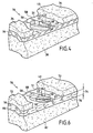
- the figure 4 represents in perspective the case of the figure 3B , references 34, 36, 38 having the same meaning as on the Figure 2B .
- the two half-cylinders 58 and 68 pass through the insulating layer 36, in a direction perpendicular to the plane of this layer and to the plane of the silicon surface layer 34.
- the figure 5 represents an SOI structure 70 in which the silicon surface layer 72 and the insulator or oxide layer 74 have been treated by the ion flux only to a depth identified by the plane 76 (zone or plane of impantation of ions).
- the insulator or silicon dioxide layer is divided into an upper portion 78 which has been traversed by the flow of ions and a portion 80 not traversed by the flow of ions.
- the etching speed will then be different in these two zones, which makes it possible to produce etched patterns having section or diameter variations along an axis perpendicular to plane 76 or to the plane of layer 72 and layer 78.
- the figure 6 represents in perspective the result of an etching of the insulating layer 74.
- the etched area 88 is similar to the etched area 58 of the figure 4 , but on a reduced thickness with respect to the total thickness of the layer 36.
- two portions of insulation located at two distinct depths, are also etched (next to each of the etched areas 88 and 90), but at the same speed because they are both in a non-implanted region. They both have the same diameter or the same dimension and they constitute the engraved area 98.
- the invention makes it possible to define in an insulating layer such as the layer 4 of the figure 1 regions for which the etching rates of this layer are different from one region to another.
- the insulating layer then has at least a first and a second region, respectively having first and second etch rates which are different from each other.
- the point or the place where the etching begins may be located in a non-implanted zone, the etching then propagating in a zone implanted at a speed different from the etching in the non-implanted area.
- the combination of the various embodiments mentioned above makes it possible to produce etched areas having different dimensions in two or three directions of space. So, in the case of the figure 6 , the diameter or the largest dimension or the characteristic dimension in each portion or etched area, or the section of this portion or etched area, varies both in the plane of the layer 74, and in a direction perpendicular to this plane.
- One and / or the other of these zones may be of square section (as on the figure 3C ) or be cylindrical ( figure 3A ) or semi-cylindrical ( figure 3B ). Other forms can still be made, depending on the shape of the mask initially chosen for the implantation and the point or place where the etching begins in the implanted region or outside thereof.
- a cavity having, in a parallel plane or mean plane of the insulating layer, an elliptical or polygonal section, or a part that is elliptical and partly polygonal.
- the atomic implantation zone may in fact be of totally arbitrary, convex, concave shape or any other form. This The shape of the atomic implantation zone is related to the final shape of the desired cavity.
- electronic components for example transistors, may then be made in the silicon surface layer 2, 34, 72.
- the zone etched in the insulating layer makes it possible, for example, to make a conductive portion of such a component.
- the SiO 2 material can be used as an insulator of an SOI structure.
- the invention however also applies to other insulating materials, such as for example Si3N4, SiGe, diamond, or sapphire. It also applies to any material with a high K-value, such as those described in MRS Bulletin, March 2002, Vol. 27, No.3, in an article entitled "Alternative Gate Dielectrics for Microelectronics” ; such materials are, for example, Haffnium oxide (HfO 2), or zirconium oxide (ZrO 2), alumina (Al 2 O 3), or Y 2 O 3 (ytterbium oxide).
- HfO 2 Haffnium oxide
- ZrO 2 zirconium oxide
- Al 2 O 3 alumina
- Y 2 O 3 ytterbium oxide
Abstract
Description
L'invention concerne le domaine de la réalisation de composants ou d'éléments semiconducteurs, en particulier à partir de composants ou éléments de type SOI (abréviation de Silicon on Insulator, ou Silicium sur Isolant).The invention relates to the field of the production of components or semiconductor elements, in particular from components or elements of the SOI type (abbreviation of Silicon on Insulator or Silicon on Insulator).
Le document
Dans certains cas ou certaines applications, on souhaite réaliser une ou plusieurs cavités dans un substrat en silicium ou en matériau semi-conducteur.In some cases or certain applications, it is desired to make one or more cavities in a substrate made of silicon or semiconductor material.
Par cavité, on entend un volume évidé surplombé par une couche de matériau semi-conducteur.Cavity means a hollow volume overhung by a layer of semiconductor material.
Il y a actuellement en outre un besoin de composants ou d'éléments ou de structures présentant de telles cavités.There is currently also a need for components or elements or structures having such cavities.
L'invention a tout d'abord pour objet un procédé de réalisation d'une structure semiconductrice, selon la revendication 1.The invention firstly relates to a method for producing a semiconductor structure according to claim 1.
Une telle structure peut être réalisée à partir d'une structure SOI.Such a structure can be realized from an SOI structure.
Selon l'invention, la vitesse de gravure de la couche d'isolant, après que celui-ci ait subi une implantation atomique, est plus importante que la vitesse de gravure d'un isolant vierge.According to the invention, the etching rate of the insulating layer, after it has undergone atomic implantation, is greater than the etching rate of a virgin insulator.
L'invention permet donc de définir des régions ou des zones de la couche d'isolant ayant des vitesses de gravure différentes.The invention thus makes it possible to define regions or zones of the insulating layer having different etching rates.
L'implantation atomique peut être réalisée à travers toute l'épaisseur de la couche d'isolant, ou à travers une partie seulement de cette couche, formant alors une partie supérieure d'isolant traversée par les ions et une partie inférieure d'isolant non traversée par les ions.The atomic implantation can be carried out through the entire thickness of the insulating layer, or through only a part of this layer, then forming an upper part of insulation traversed by the ions and a lower part of insulator. crossed by the ions.
Au moins un trou peut être formé dans la couche superficielle de silicum, débouchant dans la couche d'isolant, par exemple à l'intérieur d'une zone traversée par l'implantation atomique, ou à la limite d'une zone traversée par l'implantation atomique et d'une zone non traversée par l'implantation atomique, ou dans une zone de forme concave, convexe ou polygonale, et traversée par l'implantation atomique.At least one hole may be formed in the surface layer of silicum, opening into the insulating layer, for example within an area traversed by the atomic implantation, or at the limit of an area crossed by the atomic implantation and a zone not traversed by the atomic implantation, or in a zone of concave, convex or polygonal shape, and traversed by the atomic implantation.
Le matériau isolant peut être par exemple choisi parmi le dioxyde de silicium (Si02), le nitrure de silicium (Si3N4), le diamant, le saphir, l'oxyde de hafnium (Hf02), l'oxyde de zirconium (ZrO2), l'alumine (Al203), l'oxyde de lanthane (La203), l'oxyde d'ytterbium (Y203).The insulating material may for example be chosen from silicon dioxide (SiO 2), silicon nitride (Si 3 N 4), diamond, sapphire, hafnium oxide (HfO 2), zirconium oxide (ZrO 2), alumina (Al 2 O 3), lanthanum oxide (La 2 O 3), ytterbium oxide (Y 2 O 3).
L'étape de gravure étant réalisée à l'aide d'un acide, mais peut aussi être une étape de gravure sèche ou humide.The etching step is performed using an acid, but can also be a dry etching step or wet.
L'invention concerne également une structure semiconductrice selon la revendication 14.The invention also relates to a semiconductor structure according to claim 14.
La zone d'implantation atomique selon la revendication 14 peut, par exemple, avoir dans un plan parallèle au plan moyen de ladite couche isolante enterrée une forme concave ou convexe ou encore être de forme polygonale. Toute autre forme peut être réalisée.The atomic implantation zone according to claim 14 may, for example, have in a plane parallel to the mean plane of said buried insulating layer a concave or convex shape or be of polygonal shape. Any other form can be realized.
Une cavité peut être formée dans la couche d'isolant. Par exemple, une partie au moins de ladite cavité est formée dans une portion de la couche d'isolant traversée par les ions de l'implantation atomique.A cavity may be formed in the insulation layer. For example, at least a portion of said cavity is formed in a portion of the insulation layer traversed by the ions of the atomic implantation.
Cette cavité peut être par exemple de forme cylindrique, ou semi-cylindrique. D'autres formes peuvent être réalisées telles que des formes ayant, selon un plan parallèle au plan moyen de la couche d'isolant, une section au moins partiellement elliptique et/ou au moins partiellement polygonale.This cavity may for example be cylindrical or semi-cylindrical. Other shapes can be made such as shapes having, in a plane parallel to the mean plane of the insulation layer, an at least partially elliptical section and / or at least partially polygonal.
Selon un autre aspect, ladite cavité comporte une première zone ayant un premier diamètre, ou une première dimension maximale ou caractéristique, et une deuxième zone, ayant un deuxième diamètre, ou une deuxième dimension maximale ou caractéristique, différent(e) du premier.In another aspect, said cavity comprises a first zone having a first diameter, or a first maximum or characteristic dimension, and a second zone, having a second diameter, or a second maximum or characteristic dimension, different from the first one.
Ces première et deuxième zones peuvent être situées à des profondeurs moyennes différentes dans la couche d'isolant.These first and second zones may be located at different average depths in the insulation layer.
L'invention a aussi pour objet une structure semiconductrice, comportant, dans un substrat de silicium :
- une couche de silicium superficiel,
- une couche isolante enterrée, en un matériau isolant, formée sous la couche superficielle de silicium,
- une cavité, formée dans la couche d'isolant, cette cavité comportant une première zone ayant un premier diamètre, ou une première dimension maximale ou caractéristique, et une deuxième zone, ayant un deuxième diamètre, ou une deuxième dimension maximale ou caractéristique, différent(e) du premier.
- a layer of superficial silicon,
- a buried insulating layer, made of an insulating material, formed under the surface layer of silicon,
- a cavity formed in the insulating layer, said cavity having a first zone having a first diameter or a maximum or characteristic first dimension, and a second zone having a second diameter or a second maximum or characteristic dimension different ( e) of the first.
Ces deux zones peuvent être situées à une même profondeur dans la couche d'isolant, ou à des profondeurs moyennes différentes dans la couche d'isolant.These two zones may be located at the same depth in the insulation layer, or at different average depths in the insulation layer.
-
la
figure 1 représente un substrat SOI avec une implantation d'ions dans le substrat,thefigure 1 represents an SOI substrate with ion implantation in the substrate, -
les
figures 2A à 2C représentent différentes étapes d'un procédé selon l'invention,theFIGS. 2A to 2C represent different stages of a process according to the invention, -
les
figures 3A à 3C représentent différentes vues de dessus de structures obtenues à l'aide d'un procédé selon l'invention,theFIGS. 3A to 3C represent different top views of structures obtained using a method according to the invention, -
la
figure 4 est une vue en perspective de la structure représentée en vue de dessus sur lafigure 3B ,thefigure 4 is a perspective view of the structure shown in plan view on thefigure 3B , -
les
figures 5 et6 représentent une vue en coupe et une vue en perspective d'une structure obtenue à l'aide d'un procédé selon l'invention.thefigures 5 and6 represent a sectional view and a perspective view of a structure obtained using a method according to the invention.
La
Une telle structure SOI comporte une couche 2 de silicium, de préférence monocristallin, dans laquelle peuvent être réalisés les composants proprement dits, et sous laquelle est formée une couche enterrée 4 d'un isolant, par exemple de l'oxyde de silicium.Such an SOI structure comprises a layer 2 of silicon, preferably monocrystalline, in which the components themselves can be made, and in which is formed a buried
Cette couche isolante 4 constitue une isolation vis-à-vis des courants parasites et des charges provenant de particules ionisées. Elle permet aussi une bonne isolation de composants voisins réalisés dans la même couche de silicium 2, et notamment une diminution sensible des capacités parasites entre de tels composants voisins. Elle repose elle-même sur un substrat 6 en un matériau choisi parmi les matériaux semiconducteurs, par exemple le silicium, qui joue le rôle de support mécanique.This insulating
La couche superficielle de silicium a par exemple une épaisseur d'environ 10 à 500nm ou à 1000 nm ou à 3000 nm, tandis que la couche d'isolant a par exemple une épaisseur de l'ordre de quelques centaines de nm, par exemple comprise entre 100 nm ou 200 nm et 400 nm ou 500 nm.For example, the surface layer of silicon has a thickness of about 10 to 500 nm or 1000 nm or 3000 nm, while the insulation layer has for example a thickness of the order of a few hundred nm, for example included between 100 nm or 200 nm and 400 nm or 500 nm.
Ces épaisseurs, et notamment celle de la couche d'isolant, peuvent varier.These thicknesses, and in particular that of the insulating layer, may vary.
Selon l'invention, une implantation atomique de cette structure est réalisée par des espèces atomiques ou ioniques, par exemple des espèces hydrogène ou hélium, telles que H+ ou H2 + ou He2+, à une profondeur située au moins dans la couche d'isolant, par exemple ou en-dessous de la couche d'isolant. Cette implantation d'espèces atomiques engendre des défauts dans la portion de cette couche qu'elle a traversée.According to the invention, an atomic implantation of this structure is carried out by atomic or ionic species, for example hydrogen or helium species, such as H + or H 2 + or He 2+ , at a depth located at least in the layer. insulation, for example or below the insulation layer. This implantation of atomic species causes defects in the portion of this layer that it has crossed.
Ainsi, sur la
Après implantation, la gravure de l'isolant enterré peut être réalisée, par exemple à l'aide d'un acide tel que l'acide fluorhydrique HF introduit par un trou 22 (représenté en traits interrompus sur la
Les
L'implantation d'espèces atomiques est réalisée sur la plaque, à travers l'ouverture du masque (
Sur la
Après élimination du masque d'implantation, un trou débouchant 40 est réalisé au moyen des techniques de gravure classiques de la microélectronique (
Enfin, sous l'action de l'acide HF, une gravure sélective de l'isolant ou de l'oxyde enterré est réalisée au travers de ce trou débouchant, pour amener à la formation de la cavité souhaitée 50.Finally, under the action of the HF acid, a selective etching of the buried insulator or oxide is performed through this opening hole, to bring about the formation of the desired
La
Sur cette figure, comme sur les
La référence 40 désigne la zone implantée de ce substrat, la zone non implantée étant désignée par la référence 41. Dans cette structure, le trou débouchant, pratiqué dans le substrat, est désigné par la référence 42 et est localisé au coeur de la zone implantée 40.The
La gravure est réalisée progressivement dans la zone implantée et plus rapidement que dans une zone non implantée. Par exemple, sur la
La
La gravure progresse alors à la fois dans ces deux zones, 50, 51. Les vitesses de gravure dans ces deux zones sont cependant différentes l'une de l'autre. Pour cette raison, la zone gravée 54 dans la zone implantée 50 est, après une durée ΔT, plus large que la zone correspondante 64 dans la région non implantée 51.Etching progresses both in these two areas, 50, 51. The etching rates in these two areas are however different from each other. For this reason, the engraved
De même, après une durée de 2ΔT, la région gravée 56 est plus large que la région gravée 66 et, après une durée 3ΔT, la région 58 est plus large que la région 68.Likewise, after a duration of 2ΔT, the etched region 56 is wider than the etched
La
La
La
La
Il est ainsi possible de réaliser des zones gravées situées à des profondeurs, ou à des profondeurs moyennes, identiques ou différentes dans la couche d'isolant d'une structure SOI, ces profondeurs étant comptées à partir de la limite supérieure de la couche d'isolant, limite qui est en contact avec la couche superficielle 34, 72 de silicium, ou à partir de la surface supérieure de la couche de silicium superficiel.It is thus possible to produce etched areas located at depths, or at average depths, identical or different, in the insulating layer of an SOI structure, these depths being counted from the upper limit of the layer of insulation, which is in contact with the
Selon un autre aspect, l'invention permet de définir dans une couche isolante telle que la couche 4 de la
Selon encore un autre mode de réalisation, non représenté sur les figures, le point ou le lieu où commence la gravure peut être situé dans une zone non implantée, la gravure se propageant ensuite dans une zone implantée à une vitesse différente de la gravure dans la zone non implantée.According to yet another embodiment, not shown in the figures, the point or the place where the etching begins may be located in a non-implanted zone, the etching then propagating in a zone implanted at a speed different from the etching in the non-implanted area.
La combinaison des divers modes de réalisation évoqués ci-dessus permet de réaliser des zones gravées ayant des dimensions différentes suivant deux ou trois directions de l'espace. Ainsi, dans le cas de la
On peut ainsi réaliser, dans une couche d'isolant d'une structure SOI, au moins deux zones gravées présentant un premier diamètre ou une première dimension maximale ou caractéristique, un deuxième diamètre, ou une deuxième dimension maximale, différent(e) du premier diamètre ou de la première dimension maximale ou caractéristique, et éventuellement situé(e)s à des profondeurs différentes dans la couche d'isolant.It is thus possible to produce, in an insulating layer of an SOI structure, at least two etched areas having a first diameter or a maximum or characteristic first dimension, a second diameter, or a second maximum dimension, different from the first diameter or first dimension maximum or characteristic, and possibly located (s) at different depths in the layer of insulation.
L'une et/ou l'autre de ces zones peut être de section carrée (comme sur la
On peut aussi réaliser une cavité ayant, dans un plan parallèle ou plan moyen de la couche d'isolant, une section elliptique ou polygonale, ou en partie elliptique et en partie polygonale.It is also possible to produce a cavity having, in a parallel plane or mean plane of the insulating layer, an elliptical or polygonal section, or a part that is elliptical and partly polygonal.
Par ailleurs, la zone d'implantation atomique peut être en fait de forme totalement quelconque, convexe, concave ou tout autre. Cette forme de la zone d'implantation atomique est liée à la forme finale de la cavité souhaitée.Moreover, the atomic implantation zone may in fact be of totally arbitrary, convex, concave shape or any other form. This The shape of the atomic implantation zone is related to the final shape of the desired cavity.
Quel que soit le mode de réalisation envisagé, des composants électroniques, par exemple des transistors, peuvent ensuite être réalisés dans la couche superficielle 2, 34, 72 de silicium.Whatever the embodiment envisaged, electronic components, for example transistors, may then be made in the
La zone gravée dans la couche d'isolant permet par exemple de réaliser une portion conductrice d'un tel composant.The zone etched in the insulating layer makes it possible, for example, to make a conductive portion of such a component.
Le matériau Si02 peut être utilisé en tant qu'isolant d'une structure SOI.The SiO 2 material can be used as an insulator of an SOI structure.
L'invention s'applique cependant aussi à d'autres matériaux isolants, tels que par exemple le Si3N4, le SiGe, le diamant, ou le saphir. Elle s'applique également à tout matériau à coefficient K élevé, comme ceux décrits dans le
Claims (20)
- A method of making a semiconductor structure comprising a surface layer of silicon (2, 34, 72), a buried insulating layer (4, 36, 74), and a substrate (6, 38, 82), characterized in that said method comprises the following steps:- a step of implanting atoms into the semiconductor structure, implantation being performed on a determined zone of the structure and to a depth going at least as far as the insulating layer so as to define regions in the insulating layer with different etching speeds; and- a step of selectively etching the insulating layer through which atoms have been implanted so as to form a cavity in the insulating layer which extends beneath the surface layer of silicon.
- A method according to claim 2, in which atoms are implanted through the entire thickness of the insulating layer.
- A method according to claim 1, in which atoms are implanted through a fraction only of the thickness of the insulating layer.
- A method according to any one of claims 1 to 3, in which the implanting step is a step of implanting ions of hydrogen or ions of helium.
- A method according to any one of claims 1 to 4, including a step of forming at least one hole (40) in the surface layer of silicon, the hole leading into the insulating layer.
- A method according to claim 5, in which the hole (40) leads into a zone through which atoms have been implanted.
- A method according to claim 5, in which the hole leads to the boundary between a zone (50) through which atoms have been implanted and a zone (51) through which atoms have not been implanted.
- A method according to claim 5 or claim 6, the hole leading into a zone (60) through which atoms have been implanted, said zone being concave or convex in shape.
- A method according to claim 5 or claim 6, the hole leading into a zone through which atoms have been implanted, said zone being polygonal in shape.
- A method according to claim 5, the hole leading into a zone through which atoms have not been implanted.
- A method according to any one of claims 1 to 10, the insulating material being selected from: silicon dioxide (SiO2); silicon nitride (Si3N4); diamond; sapphire; hafnium oxide (HfO2); zirconium oxide (ZrO2); alumina (Al2O3); lanthanum oxide (La2O3); and ytterbium oxide (Y2O3).
- A method according to any one of claims 1 to 11, in which the etching step is performed using an acid.
- A method according to any one of claims 1 to 12, in which the etching step is a wet or dry etching step.
- A semiconductor structure comprising, in a silicon substrate:- a surface layer of silicon (2, 34, 72);- a buried insulating layer (4, 36, 78) of insulating material formed beneath the surface layer of silicon;
characterized by:- a zone (18) in which atoms have been implanted in the insulating layer or beneath said insulating layer; and- a cavity (50) formed in at least a part of the zone in which atoms have been implanted in the insulating layer, and extending laterally beneath the surface layer of silicon. - A semiconductor structure according to claim 14, the zone in which atoms have been implanted being concave, or convex, or polygonal in shape in a plane parallel to the mean plane of said buried insulating layer.
- A semiconductor structure according to claim 15, in which a portion of said cavity is formed in a part of the insulating layer through which ions for implanting atoms have not passed.
- A semiconductor structure according to claim 15 or claim 16, in which said cavity is of cylindrical shape, or semicylindrical, or of square section shape.
- A semiconductor structure according to any one of claims 15 to 17, in which the section of the cavity in a plane parallel to the mean plane of the insulating layer is elliptical or polygonal or partially elliptical and partially polygonal.
- A semiconductor structure according to any one of claims 15 to 18, said cavity comprising a first zone (58, 88) having a first diameter or a first maximum or characteristic dimension, and a second zone (68, 90, 98) having a second diameter or a second maximum or characteristic dimension, different from the first.
- A semiconductor structure according to claim 19, the first and second zones being situated at different mean depths in the insulating layer.
Applications Claiming Priority (5)
| Application Number | Priority Date | Filing Date | Title |
|---|---|---|---|
| FR0216409A FR2849269B1 (en) | 2002-12-20 | 2002-12-20 | METHOD FOR PRODUCING CAVITIES IN A SILICON PLATE |
| FR0216409 | 2002-12-20 | ||
| US44812403P | 2003-02-20 | 2003-02-20 | |
| US448124P | 2003-02-20 | ||
| PCT/FR2003/003820 WO2004059725A1 (en) | 2002-12-20 | 2003-12-19 | Method of the production of cavities in a silicon sheet |
Publications (2)
| Publication Number | Publication Date |
|---|---|
| EP1573802A1 EP1573802A1 (en) | 2005-09-14 |
| EP1573802B1 true EP1573802B1 (en) | 2008-11-26 |
Family
ID=32683899
Family Applications (1)
| Application Number | Title | Priority Date | Filing Date |
|---|---|---|---|
| EP03799651A Expired - Lifetime EP1573802B1 (en) | 2002-12-20 | 2003-12-19 | Method of the production of cavities in a silicon sheet |
Country Status (5)
| Country | Link |
|---|---|
| EP (1) | EP1573802B1 (en) |
| AT (1) | ATE415703T1 (en) |
| AU (1) | AU2003299368A1 (en) |
| DE (1) | DE60324960D1 (en) |
| WO (1) | WO2004059725A1 (en) |
Families Citing this family (5)
| Publication number | Priority date | Publication date | Assignee | Title |
|---|---|---|---|---|
| WO2005083775A1 (en) * | 2004-02-19 | 2005-09-09 | International Business Machines Corporation | FORMATION OF PATTERNED SILICON-ON-INSULATOR (SOI)/SILICON-ON-NOTHING (SON) COMPOSITE STRUCTURE BY POROUS Si ENGINEERING |
| FR2875947B1 (en) * | 2004-09-30 | 2007-09-07 | Tracit Technologies | NOVEL STRUCTURE FOR MICROELECTRONICS AND MICROSYSTEMS AND METHOD OF MAKING SAME |
| FR2876220B1 (en) | 2004-10-06 | 2007-09-28 | Commissariat Energie Atomique | METHOD FOR PRODUCING MIXED STACKED STRUCTURES, VARIOUS INSULATING AREAS AND / OR LOCALIZED VERTICAL ELECTRICAL CONDUCTION ZONES. |
| FR2897982B1 (en) | 2006-02-27 | 2008-07-11 | Tracit Technologies Sa | METHOD FOR MANUFACTURING PARTIALLY-LIKE STRUCTURES, COMPRISING AREAS CONNECTING A SURFACE LAYER AND A SUBSTRATE |
| FR3000601B1 (en) * | 2012-12-28 | 2016-12-09 | Commissariat Energie Atomique | METHOD FOR FORMING SPACERS OF A GRID OF A TRANSISTOR |
Family Cites Families (6)
| Publication number | Priority date | Publication date | Assignee | Title |
|---|---|---|---|---|
| US4956314A (en) * | 1989-05-30 | 1990-09-11 | Motorola, Inc. | Differential etching of silicon nitride |
| JPH06132262A (en) * | 1992-10-22 | 1994-05-13 | Hitachi Ltd | Method for etching thin film |
| FR2700065B1 (en) * | 1992-12-28 | 1995-02-10 | Commissariat Energie Atomique | Method of manufacturing accelerometers using silicon on insulator technology. |
| US5976945A (en) * | 1997-11-20 | 1999-11-02 | Vanguard International Semiconductor Corporation | Method for fabricating a DRAM cell structure on an SOI wafer incorporating a two dimensional trench capacitor |
| US6335292B1 (en) * | 1999-04-15 | 2002-01-01 | Micron Technology, Inc. | Method of controlling striations and CD loss in contact oxide etch |
| FR2795554B1 (en) * | 1999-06-28 | 2003-08-22 | France Telecom | HOLES LATERAL ENGRAVING METHOD FOR MANUFACTURING SEMICONDUCTOR DEVICES |
-
2003
- 2003-12-19 EP EP03799651A patent/EP1573802B1/en not_active Expired - Lifetime
- 2003-12-19 AU AU2003299368A patent/AU2003299368A1/en not_active Abandoned
- 2003-12-19 AT AT03799651T patent/ATE415703T1/en not_active IP Right Cessation
- 2003-12-19 DE DE60324960T patent/DE60324960D1/en not_active Expired - Lifetime
- 2003-12-19 WO PCT/FR2003/003820 patent/WO2004059725A1/en active Application Filing
Also Published As
| Publication number | Publication date |
|---|---|
| DE60324960D1 (en) | 2009-01-08 |
| AU2003299368A1 (en) | 2004-07-22 |
| WO2004059725A1 (en) | 2004-07-15 |
| EP1573802A1 (en) | 2005-09-14 |
| ATE415703T1 (en) | 2008-12-15 |
Similar Documents
| Publication | Publication Date | Title |
|---|---|---|
| EP1058946B1 (en) | Method for forming cavities in a semiconductor substrate by implanting atoms | |
| EP1797587B1 (en) | Method for providing mixed stacked structures, with various insulating zones and/or electrically conducting zones vertically localized | |
| FR2842650A1 (en) | Fabrication of substrates for optics, electronics, or optoelectronics, by implanting atomic species beneath front face of ingot to create zone of weakness, bonding support, and directly detaching portion of top layer bonded to support | |
| FR2489041A1 (en) | METHOD OF FORMING AN EVIDENCE IN A SEMICONDUCTOR BODY | |
| EP1811560A1 (en) | Method of manufacturing a composite substrate with improved electrical properties | |
| EP3646374B1 (en) | Process for transferring a thin layer to a support substrate that have different thermal expansion coefficients | |
| WO2004109781A1 (en) | Substrate for stressed systems and method for crystal growth on such a substrate | |
| WO2001009944A1 (en) | Method for producing via-connections in a substrate and substrate equipped with same | |
| FR2849269A1 (en) | Production of semiconductor structure with cavities in silicon substrate, comprises atomic implantation across buried insulating layer | |
| FR2888400A1 (en) | Film producing method for e.g. optic application, involves selectively implanting atomic species via face of wafer for forming implanted zone at predefined depth, and forming protective layer in horizontal walls of step | |
| EP2840589B1 (en) | Improved separation method between an active area of a substrate and the rear surface thereof or a portion of the rear surface thereof | |
| FR2969664A1 (en) | METHOD FOR CLEAVING A SUBSTRATE | |
| WO2008074862A1 (en) | Method for forming microwires and/or nanowires | |
| EP2612352B1 (en) | Process for producing a film, for example a single-crystal film, on a polymer substrate | |
| EP1573802B1 (en) | Method of the production of cavities in a silicon sheet | |
| FR2839199A1 (en) | METHOD OF MANUFACTURING SUBSTRATES WITH DETACHMENT OF A TEMPORARY SUPPORT, AND ASSOCIATED SUBSTRATE | |
| EP2332171B1 (en) | Process for fabricating a semiconductor structure with a buried ground plane | |
| EP1631982A1 (en) | Method for production of a very thin layer with thinning by means of induced self-support | |
| EP1428247B1 (en) | Production method for field-effect transistor with horizontal self-aligned gates | |
| FR2842647A1 (en) | LAYER TRANSFER METHOD | |
| FR2969373A1 (en) | METHOD OF ASSEMBLING TWO PLATES AND CORRESPONDING DEVICE | |
| EP3948941B1 (en) | Method for manufacturing a semiconductor-on-insulator substrate | |
| WO2005013338A2 (en) | Production of a structure comprising a protective layer against chemical treatment | |
| FR3115278A1 (en) | Membrane Transfer Process | |
| FR2912550A1 (en) | Strained silicon on insulator structure/plate fabricating method, involves contacting germanium layer with silicon layer which presents germanium concentration of thirty percent and duration of over-etching phase lower than twenty seconds |
Legal Events
| Date | Code | Title | Description |
|---|---|---|---|
| PUAI | Public reference made under article 153(3) epc to a published international application that has entered the european phase |
Free format text: ORIGINAL CODE: 0009012 |
|
| 17P | Request for examination filed |
Effective date: 20050606 |
|
| AK | Designated contracting states |
Kind code of ref document: A1 Designated state(s): AT BE BG CH CY CZ DE DK EE ES FI FR GB GR HU IE IT LI LU MC NL PT RO SE SI SK TR |
|
| AX | Request for extension of the european patent |
Extension state: AL LT LV MK |
|
| DAX | Request for extension of the european patent (deleted) | ||
| GRAP | Despatch of communication of intention to grant a patent |
Free format text: ORIGINAL CODE: EPIDOSNIGR1 |
|
| GRAS | Grant fee paid |
Free format text: ORIGINAL CODE: EPIDOSNIGR3 |
|
| GRAA | (expected) grant |
Free format text: ORIGINAL CODE: 0009210 |
|
| AK | Designated contracting states |
Kind code of ref document: B1 Designated state(s): AT BE BG CH CY CZ DE DK EE ES FI FR GB GR HU IE IT LI LU MC NL PT RO SE SI SK TR |
|
| REG | Reference to a national code |
Ref country code: GB Ref legal event code: FG4D Free format text: NOT ENGLISH |
|
| REG | Reference to a national code |
Ref country code: CH Ref legal event code: EP |
|
| REG | Reference to a national code |
Ref country code: IE Ref legal event code: FG4D Free format text: LANGUAGE OF EP DOCUMENT: FRENCH |
|
| REF | Corresponds to: |
Ref document number: 60324960 Country of ref document: DE Date of ref document: 20090108 Kind code of ref document: P |
|
| PG25 | Lapsed in a contracting state [announced via postgrant information from national office to epo] |
Ref country code: ES Free format text: LAPSE BECAUSE OF FAILURE TO SUBMIT A TRANSLATION OF THE DESCRIPTION OR TO PAY THE FEE WITHIN THE PRESCRIBED TIME-LIMIT Effective date: 20090308 Ref country code: AT Free format text: LAPSE BECAUSE OF FAILURE TO SUBMIT A TRANSLATION OF THE DESCRIPTION OR TO PAY THE FEE WITHIN THE PRESCRIBED TIME-LIMIT Effective date: 20081126 |
|
| PG25 | Lapsed in a contracting state [announced via postgrant information from national office to epo] |
Ref country code: FI Free format text: LAPSE BECAUSE OF FAILURE TO SUBMIT A TRANSLATION OF THE DESCRIPTION OR TO PAY THE FEE WITHIN THE PRESCRIBED TIME-LIMIT Effective date: 20081126 Ref country code: SI Free format text: LAPSE BECAUSE OF FAILURE TO SUBMIT A TRANSLATION OF THE DESCRIPTION OR TO PAY THE FEE WITHIN THE PRESCRIBED TIME-LIMIT Effective date: 20081126 |
|
| BERE | Be: lapsed |
Owner name: S.O.I. TEC SILICON ON INSULATOR TECHNOLOGIES Effective date: 20081231 |
|
| REG | Reference to a national code |
Ref country code: IE Ref legal event code: FD4D |
|
| PG25 | Lapsed in a contracting state [announced via postgrant information from national office to epo] |
Ref country code: MC Free format text: LAPSE BECAUSE OF NON-PAYMENT OF DUE FEES Effective date: 20081231 Ref country code: IE Free format text: LAPSE BECAUSE OF FAILURE TO SUBMIT A TRANSLATION OF THE DESCRIPTION OR TO PAY THE FEE WITHIN THE PRESCRIBED TIME-LIMIT Effective date: 20081126 Ref country code: DK Free format text: LAPSE BECAUSE OF FAILURE TO SUBMIT A TRANSLATION OF THE DESCRIPTION OR TO PAY THE FEE WITHIN THE PRESCRIBED TIME-LIMIT Effective date: 20081126 Ref country code: RO Free format text: LAPSE BECAUSE OF FAILURE TO SUBMIT A TRANSLATION OF THE DESCRIPTION OR TO PAY THE FEE WITHIN THE PRESCRIBED TIME-LIMIT Effective date: 20081126 Ref country code: BG Free format text: LAPSE BECAUSE OF FAILURE TO SUBMIT A TRANSLATION OF THE DESCRIPTION OR TO PAY THE FEE WITHIN THE PRESCRIBED TIME-LIMIT Effective date: 20090226 Ref country code: EE Free format text: LAPSE BECAUSE OF FAILURE TO SUBMIT A TRANSLATION OF THE DESCRIPTION OR TO PAY THE FEE WITHIN THE PRESCRIBED TIME-LIMIT Effective date: 20081126 |
|
| REG | Reference to a national code |
Ref country code: CH Ref legal event code: PL |
|
| PG25 | Lapsed in a contracting state [announced via postgrant information from national office to epo] |
Ref country code: SE Free format text: LAPSE BECAUSE OF FAILURE TO SUBMIT A TRANSLATION OF THE DESCRIPTION OR TO PAY THE FEE WITHIN THE PRESCRIBED TIME-LIMIT Effective date: 20090226 Ref country code: CZ Free format text: LAPSE BECAUSE OF FAILURE TO SUBMIT A TRANSLATION OF THE DESCRIPTION OR TO PAY THE FEE WITHIN THE PRESCRIBED TIME-LIMIT Effective date: 20081126 Ref country code: PT Free format text: LAPSE BECAUSE OF FAILURE TO SUBMIT A TRANSLATION OF THE DESCRIPTION OR TO PAY THE FEE WITHIN THE PRESCRIBED TIME-LIMIT Effective date: 20090427 |
|
| PG25 | Lapsed in a contracting state [announced via postgrant information from national office to epo] |
Ref country code: BE Free format text: LAPSE BECAUSE OF NON-PAYMENT OF DUE FEES Effective date: 20081231 Ref country code: SK Free format text: LAPSE BECAUSE OF FAILURE TO SUBMIT A TRANSLATION OF THE DESCRIPTION OR TO PAY THE FEE WITHIN THE PRESCRIBED TIME-LIMIT Effective date: 20081126 |
|
| PLBE | No opposition filed within time limit |
Free format text: ORIGINAL CODE: 0009261 |
|
| STAA | Information on the status of an ep patent application or granted ep patent |
Free format text: STATUS: NO OPPOSITION FILED WITHIN TIME LIMIT |
|
| PG25 | Lapsed in a contracting state [announced via postgrant information from national office to epo] |
Ref country code: CH Free format text: LAPSE BECAUSE OF NON-PAYMENT OF DUE FEES Effective date: 20081231 Ref country code: LI Free format text: LAPSE BECAUSE OF NON-PAYMENT OF DUE FEES Effective date: 20081231 |
|
| 26N | No opposition filed |
Effective date: 20090827 |
|
| PG25 | Lapsed in a contracting state [announced via postgrant information from national office to epo] |
Ref country code: CY Free format text: LAPSE BECAUSE OF FAILURE TO SUBMIT A TRANSLATION OF THE DESCRIPTION OR TO PAY THE FEE WITHIN THE PRESCRIBED TIME-LIMIT Effective date: 20081126 Ref country code: LU Free format text: LAPSE BECAUSE OF NON-PAYMENT OF DUE FEES Effective date: 20081219 Ref country code: HU Free format text: LAPSE BECAUSE OF FAILURE TO SUBMIT A TRANSLATION OF THE DESCRIPTION OR TO PAY THE FEE WITHIN THE PRESCRIBED TIME-LIMIT Effective date: 20090527 |
|
| PG25 | Lapsed in a contracting state [announced via postgrant information from national office to epo] |
Ref country code: TR Free format text: LAPSE BECAUSE OF FAILURE TO SUBMIT A TRANSLATION OF THE DESCRIPTION OR TO PAY THE FEE WITHIN THE PRESCRIBED TIME-LIMIT Effective date: 20081126 |
|
| PG25 | Lapsed in a contracting state [announced via postgrant information from national office to epo] |
Ref country code: GR Free format text: LAPSE BECAUSE OF FAILURE TO SUBMIT A TRANSLATION OF THE DESCRIPTION OR TO PAY THE FEE WITHIN THE PRESCRIBED TIME-LIMIT Effective date: 20090227 |
|
| PGFP | Annual fee paid to national office [announced via postgrant information from national office to epo] |
Ref country code: GB Payment date: 20101201 Year of fee payment: 8 |
|
| REG | Reference to a national code |
Ref country code: DE Ref legal event code: R082 Ref document number: 60324960 Country of ref document: DE Representative=s name: CBDL PATENTANWAELTE, DE |
|
| REG | Reference to a national code |
Ref country code: FR Ref legal event code: CD Owner name: SOITEC, FR Effective date: 20120907 |
|
| REG | Reference to a national code |
Ref country code: DE Ref legal event code: R081 Ref document number: 60324960 Country of ref document: DE Owner name: SOITEC, FR Free format text: FORMER OWNER: S.O.I. TEC SILICON ON INSULATOR TECHNOLOGIES, BERNIN, FR Effective date: 20120905 Ref country code: DE Ref legal event code: R082 Ref document number: 60324960 Country of ref document: DE Representative=s name: CBDL PATENTANWAELTE, DE Effective date: 20120905 |
|
| PGFP | Annual fee paid to national office [announced via postgrant information from national office to epo] |
Ref country code: IT Payment date: 20121123 Year of fee payment: 10 |
|
| PGFP | Annual fee paid to national office [announced via postgrant information from national office to epo] |
Ref country code: NL Payment date: 20121120 Year of fee payment: 10 |
|
| GBPC | Gb: european patent ceased through non-payment of renewal fee |
Effective date: 20121219 |
|
| PG25 | Lapsed in a contracting state [announced via postgrant information from national office to epo] |
Ref country code: GB Free format text: LAPSE BECAUSE OF NON-PAYMENT OF DUE FEES Effective date: 20121219 |
|
| REG | Reference to a national code |
Ref country code: NL Ref legal event code: V1 Effective date: 20140701 |
|
| PG25 | Lapsed in a contracting state [announced via postgrant information from national office to epo] |
Ref country code: NL Free format text: LAPSE BECAUSE OF NON-PAYMENT OF DUE FEES Effective date: 20140701 |
|
| PG25 | Lapsed in a contracting state [announced via postgrant information from national office to epo] |
Ref country code: IT Free format text: LAPSE BECAUSE OF NON-PAYMENT OF DUE FEES Effective date: 20131231 |
|
| REG | Reference to a national code |
Ref country code: FR Ref legal event code: PLFP Year of fee payment: 13 |
|
| PG25 | Lapsed in a contracting state [announced via postgrant information from national office to epo] |
Ref country code: IT Free format text: LAPSE BECAUSE OF NON-PAYMENT OF DUE FEES Effective date: 20131219 |
|
| REG | Reference to a national code |
Ref country code: FR Ref legal event code: PLFP Year of fee payment: 14 |
|
| REG | Reference to a national code |
Ref country code: FR Ref legal event code: PLFP Year of fee payment: 15 |
|
| PGFP | Annual fee paid to national office [announced via postgrant information from national office to epo] |
Ref country code: FR Payment date: 20221122 Year of fee payment: 20 Ref country code: DE Payment date: 20221102 Year of fee payment: 20 |
|
| REG | Reference to a national code |
Ref country code: DE Ref legal event code: R082 Ref document number: 60324960 Country of ref document: DE Representative=s name: CBDL PATENTANWAELTE GBR, DE |
|
| REG | Reference to a national code |
Ref country code: DE Ref legal event code: R071 Ref document number: 60324960 Country of ref document: DE |