EP1571465A2 - Method of and apparatus for producing micro lens and micro lens - Google Patents
Method of and apparatus for producing micro lens and micro lens Download PDFInfo
- Publication number
- EP1571465A2 EP1571465A2 EP05003937A EP05003937A EP1571465A2 EP 1571465 A2 EP1571465 A2 EP 1571465A2 EP 05003937 A EP05003937 A EP 05003937A EP 05003937 A EP05003937 A EP 05003937A EP 1571465 A2 EP1571465 A2 EP 1571465A2
- Authority
- EP
- European Patent Office
- Prior art keywords
- resin layer
- lens
- resin
- substrate
- solvent
- Prior art date
- Legal status (The legal status is an assumption and is not a legal conclusion. Google has not performed a legal analysis and makes no representation as to the accuracy of the status listed.)
- Granted
Links
Images



Classifications
-
- G—PHYSICS
- G02—OPTICS
- G02B—OPTICAL ELEMENTS, SYSTEMS OR APPARATUS
- G02B3/00—Simple or compound lenses
- G02B3/0006—Arrays
- G02B3/0012—Arrays characterised by the manufacturing method
- G02B3/0031—Replication or moulding, e.g. hot embossing, UV-casting, injection moulding
-
- B—PERFORMING OPERATIONS; TRANSPORTING
- B29—WORKING OF PLASTICS; WORKING OF SUBSTANCES IN A PLASTIC STATE IN GENERAL
- B29D—PRODUCING PARTICULAR ARTICLES FROM PLASTICS OR FROM SUBSTANCES IN A PLASTIC STATE
- B29D11/00—Producing optical elements, e.g. lenses or prisms
- B29D11/00009—Production of simple or compound lenses
- B29D11/00365—Production of microlenses
-
- G—PHYSICS
- G02—OPTICS
- G02B—OPTICAL ELEMENTS, SYSTEMS OR APPARATUS
- G02B3/00—Simple or compound lenses
- G02B3/0006—Arrays
- G02B3/0012—Arrays characterised by the manufacturing method
- G02B3/0018—Reflow, i.e. characterized by the step of melting microstructures to form curved surfaces, e.g. manufacturing of moulds and surfaces for transfer etching
Definitions
- This invention relates to a method of and an apparatus for producing a micro lens. This invention further relates to a method of forming a mold (mother) for forming the micro lens.
- a micro lens for increasing light collecting efficiency is provided corresponding to each of a plurality of photodetector elements such as a photodiode.
- the micro lenses form a micro lens array comprising a plurality of two-dimensionally arranged micro lenses, and the micro lens is often used in the form of a micro lens array.
- micro lens array is often used in a display and an image exposure system as a spatial light modulator element as well as the solid state image taking device.
- an example of the micro lens array of this type is disclosed.
- the curved surface can be formed only in the periphery of the pattern and the obtained micro lens does not regularly function since the central portion can be solidified before the fluidity of the resist becomes sufficient.
- the primary object of the present invention is to provide a method of producing a micro lens which can produce the micro lens at high accuracy with ease with fluctuation in the shape minimized even if it is low in height.
- a second obj ect of the present invention is to provide a method of producing a mother of a micro lens which is useful to accomplish the above object.
- a third object of the present invention is to provide an apparatus for carrying out the above method of producing the micro lens and the method of producing the mother of the micro lens.
- a resin layer is caused to absorb its solvent to have fluidity and to become convex under the surface tension without process of fusing the resin.
- the convex portion of the resin can be used as a lens if the resin is transparent. Otherwise, the convex portion of the resin can be transferred to the substrate on which it is carried and a lens may be formed in the substrate or to the member other than the substrate to form a mother for molding a lens and a lens may be formed by casting therein transparent material.
- a first method of producing a micro lens comprising the steps of
- an aspheric lens can be produced by changing the etching rates of the resin and the substrate by continuously or stepwise changing etching conditions with time during the dry etching.
- the (transparent) resin layer by patterning the (transparent) resin layer into substantially an ellipsoid or a polygon approximated thereto, a lens where the curvature in a cross-section parallel to the optical axis differs depending on the orientation can be produced.
- a plurality of the micro lenses are one-dimensionally or two-dimensionally arranged to form a lens array.
- a method of producing a micro lens forming mold comprising the steps of
- a lens forming mold for forming a lens where the curvature in a cross-section parallel to the optical axis differs depending on the orientation can be produced.
- the mold can mold a lens array by forming a plurality of one-dimensionally or two-dimensionally arranged convex portion of the resin.
- the surface of the substrate be coated with coating exhibiting liquid repellency to the resin which has absorbed the solvent and has been dissolved, from the resin layer side after forming the resin layer in a desired pattern and before causing the resin layer to absorb the solvent.
- the resin be held in the atmosphere of the solvent until the coating adhering to the surface of the resin is taken in the inside of the resin when causing the resin layer to absorb the solvent.
- the coating comprises fluorine or silicone compound.
- the coating be of silane coupling agent of fluorocarbon series.
- the surface of the substrate be treated with a surface treatment with oxygen plasma or ozone before providing the coating.
- the resin be heat-treated to be solidified after the solvent is dried.
- an apparatus for carrying out the above method of producing the micro lens and the method of producing the micro lens forming mold comprising at least
- the apparatus be further comprises a means for heating and solidifying the resin after the solvent is dried.
- the first method of producing a micro lens of the present invention since resin in a predetermined pattern is caused to absorb from its surroundings solvent which dissolves the resin so that the resin has fluidity and the surface of the resin becomes convex and a lens under the surface tension, it is unnecessary to heat the resin and accordingly, the problem that the lens becomes incorrect due to heating of resin can be avoided whereby a micro lens can be produced at a high accuracy. Further, the volume of the resin is increased and the resin becomes more apt to flow due to the fact that the resin absorbs the solvent, even a lens which is low in height can be easily produced.
- the resin can be applied to the substrate by spin coating or the like where the thickness can be accurately controlled, the volumes of the lenses which are determined by the lens region patterned, for instance, by photolithography and the thickness of the resin can be accurately controlled and a micro lens array which is less in fluctuation can be produced.
- the portion of the resin which is caused to become a lens shape in the manner as described above in conjunction with the first method is transferred to the substrate and a lens is formed on the substrate, the portion of the resin which is caused to become a lens shape can be easily shaped into even a lens which is low in height at high accuracy with less fluctuation in shape as in the first embodiment of producing a micro lens. Accordingly, the lens formed by transferring the portion of the resin to the substrate can be easily produced at high accuracy with less fluctuation in shape even if the lens is low in height.
- the substrate since the portion of the resin caused to become a lens shape is transferred to the substrate by dry-etching and the lens is formed in the substrate, the substrate whose material can be relatively freely selected as compared with the resin whose material is limited due to the steps such as the step of patterning the resin by photolithography can be used as the material of the lens. Accordingly, a micro lens which is higher in durability and less in light absorption can be produced.
- the portion of the resin which is caused to become a lens shape in the manner as described above in conjunction with the first method is transferred to another member and a lens-forming mold is formed on the member, the portion of the resin which is caused to become a lens shape can be easily shaped into even a lens which is low in height at high accuracy with less fluctuation in shape as in the first embodiment of producing a micro lens. Accordingly, the lens formed by casting a transparent member into the lens forming mold obtained by transferring the portion of the resin to the member can be easily produced at high accuracy with less fluctuation in shape even if the lens is low in height.
- the portion of the resin which is caused to become a lens shape in the manner as described above in conjunction with the first method is transferred to another member and a lens-forming mold is formed on the member, the portion of the resin which is caused to become a lens shape can be easily shaped into even a lens which is low in height at high accuracy with less fluctuation in shape as in the first embodiment of producing a micro lens. Accordingly, the lens forming mold obtained by transferring the portion of the resin to the member can be easily produced at high accuracy with less fluctuation in shape even if the lens is low in height. Accordingly, the lens formed by casting a transparent member into the lens forming mold can be easily produced at high accuracy with less fluctuation in shape even if the lens is low in height.
- the marginal temperature where the resin has fluidity is narrow, and it has been necessary to accurately control the processing conditions and/or to limit the material.
- the lens shape can be easily formed by suitably selecting the resin before solidifying and the solvent which dissolves the resin. Accordingly, the methods of producing a micro lens or a method of a micro lens forming mold in accordance with the present invention is superior to the conventional fusing method in both the freedom in selecting the material and broadness of the margin of the processing conditions.
- the material can be treated under normal temperatures in the methods of producing a micro lens in accordance with the present invention, the problem of color fading due to heat which is apt to occur when micro lenses are formed on a color filter as in on-chip lenses of a CCD can be avoided.
- the surface of the substrate is coated with coating exhibiting liquid repellency to the resin which has absorbed the solvent and has been dissolved, from the resin layer side after forming the resin layer in a desired pattern and before causing the resin layer to absorb the solvent in the method of producing a micro lens or the method of producing a micro lens forming mold in accordance with the present invention, spread of the resin when the resin is dissolved can be prevented, whereby the micro lens or the micro lens forming mold can be more accurately produced.
- the coating is prevented from remaining on the surface of lens-like portion of the resin to be transferred to said substrate or said another member whereby deterioration of the lens performance and the adverse influence on transfer by the remaining coating can be prevented.
- the coating described above when the coating described above is provided, if the surface of the substrate is treated with a surface treatment with oxygen plasma or ozone before providing the coating, organic material or the like can be removed from the surface of the substrate, whereby the coating can firmly adhere to the surface of the substrate.
- the micro lens formed by the resin and/or the lens-like portion of the resin to be transferred to said substrate or said another member can be strong.
- the methods of producing a micro lens or the method of producing a micro lens forming mold described above can be efficiently carried out.
- the apparatuses of the present invention is provided with a means for holding the substrate carrying thereon the resin layer in a treatment container, and replacing the inside of the container with inert gas or evacuating the inside of the container under vacuum, the step of causing the resin to absorb the solvent can be carried out under an oxygen-reduced atmosphere, whereby even the solvent which is low in flashpoint and/or is explosive can be treated in safety.
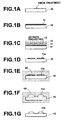
- a method of producing a micro lens in accordance with a first embodiment of the present invention will be described with reference to Figures 1A to 1G, hereinbelow.
- a surface of a transparent SiO 2 glass substrate 10 is treated with HMDS (hexamethyldisilazane) as shown in Figure 1A.
- the surface of the substrate 10 is coated with positive resist 11 of phenolic novolak series in a predetermined thickness by spin coating as shown in Figure 1B.
- the substrate 10 thus treated is soft-baked for a predetermined time at 80 to 120°C by the use of a hot plate or a clean oven.
- the resist 11 on the substrate 10 is exposed to light by a projecting exposure system or a contact aligner through a photo-mask 13 having a Cr pattern 12 of a closed curve corresponding to a cross-section defined by a desired curved surface of the lens and the substrate surface or of a polygon approximated thereto as shown in Figure 1C.
- the photo-mask 13 used here if it has a plurality of the Cr pattern 12 which are one-dimensionally or two-dimensionally arranged, can be used in production of a micro lens array, and the micro lens array is very high in dimensional accuracy since it is produced by application of the lithography.
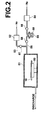
- the apparatus shown in Figure 2 comprises a purge line 53 for introducing N 2 gas (the flow rate of which is controlled by a flow control means 52) into a solvent vapor treatment container 51, a bubbler 55 which blows into solvent N 2 gas the flow rate of which is controlled by a flow control means 54, a solvent vapor introduction line 56 for introducing vapor of solvent into the solvent vapor treatment container 51, and valves 57 and 58 for connecting and disconnecting the purge line 53 and the solvent vapor introduction line 56 to and from the solvent vapor treatment container 51.
- this apparatus may be added with a heater for heating the bubbler 55 as desired and a trap for removing the solvent vapor from the discharge of the solvent vapor treatment container 51.
- the treatment by the apparatus will be described next.
- the substrate 10 provided with the resist pattern 11a is held on a substrate holding table 50 in the solvent vapor treatment container 51 and then N 2 gas is introduced into the container 51 through the purge line 53, thereby replacing the gas in the container 51 with the N 2 gas.
- N 2 gas is introduced into the container 51 through the purge line 53, thereby replacing the gas in the container 51 with the N 2 gas.
- resist thinner (ethyl lactate) 59 which is solvent of the resist pattern 11a is introduced into the bubbler 55 and while a predetermined amount of N 2 gas is flowed, the resist thinner 59 is introduced into the solvent vapor treatment container 51. If the resist thinner 59 is heated at this time, higher vapor pressure can be obtained and the time required to the treatment can be shortened. When this state is kept for a predetermined time as shown in Figure 1E, the resist pattern 11a absorbs the evaporated resist thinner 59 and is dissolved. The inside of the solvent vapor treatment container 51 is kept at the room temperature and the dissolution progresses at a low temperature of 20 to 25°C.
- the resist pattern 11a absorbs the resist thinner 59 and the dissolved resist pattern 11a comes to have fluidity, whereby the surface of the resist pattern 11a becomes convex under the surface tension as shown in Figure 1F.
- N 2 gas is introduced into the container 51 through the purge line 53, thereby replacing the gas in the container 51 with the N 2 gas.
- the resist thinner 59 absorbed by the resist pattern 11a is gradually dried and evaporated at this time and only the solid components are left there, whereby a desired lens shape is formed.
- the solid components left at this time depend upon the volume of the resist pattern 11a and does not depend upon the amount of the resist thinner 59 absorbed by the resist pattern 11a. If drying here is insufficient, the solvent abruptly evaporates during heating to be carried out later to cause generation of bubbles and/or deformation of the lens shape.
- the substrate 10 is taken out from the solvent vapor treatment container 51 and heated to 80 to 120°C by the use of a hot plate or a clean oven to remove the residual solvent. Further, the substrate 10 is heated to 150 to 200°C to solidify the resist pattern 11a. In this manner, highly hard micro lenses 11b are formed on the substrate 10 as shown in Figure 1G.
- the resist 11 is employed as a material of the lens.
- the influence on the lens performance can be avoided by projecting ultraviolet rays onto the entire area of the substrate 10 after one of the steps described above.
- the substrate 10 is heated to solidify the resist pattern 11a in the last step in this embodiment, the resist pattern 11a may be solidified by another treatment such as projection of ultraviolet rays. If there gives rise to no problem in the lens performance, the solidifying treatment may be abbreviated.
- resist 11 is employed in this embodiment, resist based on acrylic resin, epoxy resin or the like or a pattern formed by resin such polyethylene, polystyrene, polycarbonate or the like may be employed to produce a micro lens in accordance with the method of the present invention.
- an open system solvent vapor treatment apparatus may be employed by providing a solvent vapor recovery means. In this case, a continuous treatment can be carried out.
- FIG 3 shows an example of the open system solvent vapor treatment apparatus.
- the apparatus shown in Figure 3 is provided with a pair of substrate holding tables 50, a first blowing means 60 which blows the solvent vapor on the substrate 10 held on one of the substrate holding tables 50, a second blowing means 61 which blows the solvent vapor on the substrate 10 held on the other substrate holding table 50, a draft chamber 62 which accommodates therein the two substrate holding tables 50 and communicates with a discharge means (not shown) at a lower portion thereof, and a hot plate 63 which is disposed outside the draft chamber 62 and heats the substrate 10.
- the substrate 10 on which the resist pattern 11a has been formed is held on the left substrate holding table 50 and solvent vapor is blown on the substrate 10. Then the substrate 10 the surface of the resist pattern 11a on which has become convex is held on the right substrate holding table 50. Then the substrate 10 is dried while blowing N 2 gas on the substrate 10, whereby the resist thinner 59 absorbed by the resist pattern 11a is gradually evaporated with only the solid components left there and a desired lens shape is formed by the resist pattern 11a.
- the substrate 10 When the substrate 10 is placed on the hot plate 63 and the resist pattern 11a is solidified by heating the substrate 10, for instance, to 150 to 200°C, highly hard micro lenses 11b are formed on the substrate 10.
- toric lenses where the curvature in a cross-section parallel to the optical axis differs depending on the orientation, which is difficult in refractive index profile lenses by the isotropic etching or the impurity diffusion, can be produced by simply shaping the resist pattern 11a into substantially an ellipsoid or a polygon approximated thereto. This is true of the embodiments to be described hereinbelow.
- the lens shape is formed by the use of the surface tension of the resist pattern 11a having fluidity and accordingly, the lens shape becomes apt to be affected by the gravity as the lens size is increased. Taking into account this fact, the method of this embodiment is practically suitable for producing micro lenses whose diameter is about 1 to 100 ⁇ m. This is true of the embodiments to be described hereinbelow.
- the resist pattern 11a absorbs the solvent and bulges, the adjacent micro lenses are brought into contact with each other and the regular curved lens surfaces cannot be formed if the micro lenses are arranged in an array where the pitches of the micro lenses are substantially equal to L when H/L>1/2, where L represents the length of the lens in a direction perpendicular to the optical axis and H represents the height of the lens in a direction of the optical axis. Accordingly, when producing a micro lens array, it is necessary to determine the dimensions of L and H taking into account this fact. This is true of the embodiments to be described hereinbelow.
- a method of producing a micro lens in accordance with a second embodiment of the present invention will be described with reference to Figures 4A to 4F, hereinbelow.
- a resist pattern 11a of phenolic novolak series is formed on a SiO 2 glass substrate 10 in the same manner as in the first embodiment described above as shown in Figure 4A. That is, Figure 4A corresponds to Figure 1D.
- the surface of the substrate 10 on which the resist pattern 11a has been formed is treated with oxygen plasma.
- descum ashing is carried out with a plane-parallel plate oxygen plasma ashing apparatus.
- the treating conditions are, for instance, as follows. high frequency power:10 to 50W, treating time:10 to 60s, chamber pressure:1 to 30Pa
- the surface of the substrate 10 is coated with liquid repellent coating.
- a silane coupling agent of fluorocarbon series (Optool DSX: Daikin Industries, Ltd.) is employed as the coating material, and the liquid repellent coating 20 is provided in thickness of 1 to 100nm by spin coating or dipping as shown in Figure 4B. Then the substrate 10 washed in rinsing solution comprising fluorine solvent which does not dissolve the resist pattern 11a and is dried.
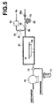
- the apparatus shown in Figure 5 comprises a solvent vapor treatment container 51 which accommodates therein a substrate holding table 50 for holding a substrate 10 and is for accomplishing the solvent vapor treatment, a purge line 53 for introducing N 2 gas (the flow rate of which is controlled by a flow control means 52) into the solvent vapor treatment container 51, a bubbler 55 which blows into solvent N 2 gas the flow rate of which is controlled by a flow control valve 58a, a solvent vapor introduction line 56 for introducing vapor of solvent into the solvent vapor treatment container 51,valves 57 and 58 for connecting and disconnecting the purge line 53 and the solvent vapor introduction line 56 to and from the solvent vapor treatment container 51, a pump 70 which evacuates the inside of the solvent vapor treatment container 51, and a trap 71 for removing the solvent
- the treatment by the apparatus will be described next.
- the substrate 10 provided with the resist pattern 11a is held on the substrate holding table 50 in the solvent vapor treatment container 51 and evacuates by the pump 70 the inside of the solvent vapor treatment container 51 to, for instance, a pressure not higher than 1kPa with both the purge line 53 and the solvent vapor introduction line 56 closed.
- acetone 72 which can dissolve the resist is introduced into the bubbler 55, and the valve 58 is opened with the flow rate of N 2 gas in the solvent vapor introduction line 56 nullified.
- the acetone 72 boils and concentrated acetone vapor is introduced into the solvent vapor treatment container 51.
- the resist pattern 11a absorbs the evaporated acetone 72 and is dissolved.
- the inside of the solvent vapor treatment container 51 is kept at the room temperature and the dissolution progresses at a low temperature of 20 to 25°C.
- the resist pattern 11a which has absorbed the acetone 72 and has been dissolved comes to have fluidity, whereby the surface of the resist pattern 11a becomes convex under the surface tension as shown in Figure 4D.
- the solvent vapor introduction line 56 is closed and the valve 57 is opened to introduce N 2 gas into the container 51, thereby replacing the gas in the container 51 with the N 2 gas.
- a three-way valve 73 is operated to switch the discharge line to that passing through the trap 71 to remove acetone vapor from discharge of the solvent vapor treatment container 51.
- the substrate 10 is taken out from the solvent vapor treatment container 51 and heated to 80 to 120°C by the use of a hot plate or a clean oven to remove acetone. Further, the substrate 10 is heated to 150 to 200°C to solidify the resist pattern 11a. In this manner, highly hard micro lenses 11b are formed on the substrate 10 as shown in Figure 4G.
- the part of the surface of the substrate 10 except the resist pattern 11a is liquid repellent and accordingly spread of the dissolved resist pattern 11a can be prevented.
- the liquid repellent coating 20 is provided on the surface of the resist pattern 11a. Further, since it may be as small as not larger than 100nm (preferably not larger than 10nm) in thickness, the solvent vapor can penetrate into the resist pattern 11a. Further, since the liquid repellent coating 20 is formed by a silane coupling agent in this embodiment, the adherence of the liquid repellent coating 20 to the surface of the resist pattern 11a is weaker than that to the surface of the substrate 10. Accordingly, the density of the coating film of the liquid repellent coating 20 can be less on the surface of the resist pattern 11a than the surface of the substrate 10 by washing by the rinse solution after the coating, whereby penetration of the solvent vapor can be increased.
- the liquid repellent coating 20 on the resist pattern 11a is broken when the resist pattern 11a absorbs the solvent and bulges.
- the liquid repellent coating 20 is left on the surface of the resist pattern 11a, the curved surface corresponding thereto is deformed, which can deteriorate the lens quality. Accordingly, the solvent vapor treatment should be carried out until the liquid repellent coating 20 is trapped into the resist pattern 11a.
- the relative amount of the liquid repellent coating 20 to the total volume of the lens can be suppressed not to greatly affect the refractive index of the lens.
- the surface of the substrate 10 is treated by ashing with oxygen plasma, the organic material can be removed from the surface of the substrate 10, if any, and the liquid repellent coating 20 can firmly adhere to the surface of the substrate 10.
- acetone which is small in molecular weight and easily penetrates the liquid repellent coating is especially useful as the solvent.
- a coating agent of fluorine series is employed, other coating agents such as a coating agent of silicone series may be employed so long as the coating is repellent to the dissolved resist and permeable to the solvent vapor. Also in this case, the result similar to this embodiment can be obtained.
- a method of producing a micro lens in accordance with a third embodiment of the present invention will be described with reference to Figures 6A to 6C, hereinbelow.
- the shape of lens-like portions formed on a substrate is transferred to the substrate and micro lenses of the same material as the substrate are formed on the substrate.
- a transparent SiO 2 glass substrate 10 on which micro lenses 11b are formed is first prepared by the method described above in the first or second embodiment.
- the solidifying treatment at high temperature on the micro lenses 11b need not be necessarily carried out.
- the micro lenses 11b since it is not necessary for the lens-like portions formed on the substrate 10 to operate as lenses, the lens-like portions may be formed by opaque resin.
- the substrate 10 is set to an induction coupling plasma etching apparatus (ICP) and anisotropic etching is carried out thereon.
- ICP induction coupling plasma etching apparatus
- the etching gas fluorine gas such as CF 4 , CHF 3 , SF 6 or the like or gas added thereto with O 2 is employed in an amount which will provide substantially 1:1 etching rate of the micro lenses 11b (that is, the positive resist 11 of phenolic novolak series) and the SiO 2 glass substrate 10.
- etching is initiated later as the thickness of the micro lenses 11b on the substrate 10 increases.
- the substrate 10 is etched as if the shape of the micro lenses 11b is transferred to the substrate 10 and micro lenses 10b are formed on the substrate 10 as shown in Figure 6C.
- micro lenses 10b of the same material as the substrate are formed on the SiO 2 glass substrate 10.
- the substrate 10 is formed of SiO 2 glass
- the shape of the micro lenses can be transferred by suitably selecting the etching conditions even if the substrate 10 is formed of resin such as acrylic resin, epoxy resin, polycarbonate or the like or other optical crystals.
- aspheric lenses where the curvature in a cross-section parallel to the optical axis locally differs by setting the etching rates of the micro lenses 11b and the SiO 2 glass substrate 10 in the dry etching or by changing the etching conditions such as the kind or compositions of the etching gas, the high frequency power, the bias voltage applied to the substrate 10, the chamber pressure or the like with time during the dry etching.
- the performance or the function of the lens can be improved by forming on the lens surfaces or the surface of the substrate 10 antireflection coating comprising a single film or a laminated film of a dielectric material or a light shielding pattern of Cr or the like and making it an alignment mark with an aperture or other members after the steps described above.
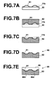
- a method of producing a micro lens in accordance with a fourth embodiment of the present invention will be described with reference to Figures 7A to 7E, hereinbelow.
- the shape of lens-like portions formed on a substrate is transferred to another member and micro lenses are formed with the member used as a lens forming mold.
- An Si substrate 80 on which micro lenses 11b are formed is first prepared by the method described above in the first or second embodiment.
- the solidifying treatment at high temperature on the micro lenses 11b need not be necessarily carried out.
- the micro lenses 11b since it is not necessary for the lens-like portions formed on the substrate 80 to operate as lenses, the lens-like portions may be formed by opaque resin.
- the substrate need not be transparent and may be an Si substrate as in this embodiment or a flat metal plate.
- the substrate 80 is set to a plane-parallel plate oxygen plasma ashing apparatus and ashing is carried out thereon.
- the treating conditions are, for instance, as follows.
- Nickel electroforming is carried out on the substrate 80 next.
- Ni separates out on the substrate 80 and a Ni plating layer 82 is formed as shown in Figure 7B.
- the nickel electroforming is continued until the thickness of the Ni plating layer 82 becomes, for instance, 0.1 to 3mm.
- the substrate 80 is taken out from the plating bath and is washed and a separating Ni mold (a Ni plating layer) is peeled off the substrate 80 as shown in Figure 7C.
- the resist (micro lenses 11b) adhering to the electroformed Ni mold 82 is removed by remover of a family of the solvent and the mold 82 is washed. This state is shown in Figure 7D. Finally, the back side of the electroformed Ni mold 82 is machined, e.g., polished and/or ground, to form a micro lens forming mold 85.
- the micro lens forming mold 85 thus formed is obtained by transferring a reverse shape of the micro lenses 11b to the electroformed Ni mold 82. Accordingly, by casting a transparent member 86 such as of transparent resin or the like into the micro lens forming mold 85 as shown in Figure 7E and removing it from the mold 86 after drying and solidifying, micro lenses 86b the same as the micro lenses 11b in shape are formed on the transparent member 86.
- electroformed mold 82 is formed of nickel in this embodiment, electroformed mold may be formed of cupper plating, plating of alloy of nickel and cobalt, or the like.
Landscapes
- Engineering & Computer Science (AREA)
- Manufacturing & Machinery (AREA)
- Physics & Mathematics (AREA)
- General Physics & Mathematics (AREA)
- Optics & Photonics (AREA)
- Health & Medical Sciences (AREA)
- Ophthalmology & Optometry (AREA)
- Mechanical Engineering (AREA)
- Chemical & Material Sciences (AREA)
- Crystallography & Structural Chemistry (AREA)
- Photosensitive Polymer And Photoresist Processing (AREA)
- Moulding By Coating Moulds (AREA)
Abstract
Description
it is unnecessary to heat the resin and accordingly, the problem that the lens becomes incorrect due to heating of resin can be avoided whereby a micro lens can be produced at a high accuracy. Further, the volume of the resin is increased and the resin becomes more apt to flow due to the fact that the resin absorbs the solvent, even a lens which is low in height can be easily produced. Further, since the resin can be applied to the substrate by spin coating or the like where the thickness can be accurately controlled, the volumes of the lenses which are determined by the lens region patterned, for instance, by photolithography and the thickness of the resin can be accurately controlled and a micro lens array which is less in fluctuation can be produced.
Accordingly, a micro lens which is higher in durability and less in light absorption can be produced.
high frequency power:10 to 50W, treating time:10 to 60s, chamber pressure:1 to 30Pa
Claims (21)
- A method of producing a micro lens comprising the steps offorming a transparent resin layer on a transparent substrate in a desired pattern,causing the resin layer to absorb from its surroundings solvent which dissolves the resin so that the resin layer has fluidity and the surface of the resin layer becomes convex under the surface tension, andthen drying the solvent to use the convex portion of the resin as a lens.
- A method of producing a micro lens comprising the steps offorming a resin layer on a transparent substrate in a desired pattern,causing the resin layer to absorb from its surroundings solvent which dissolves the resin so that the resin layer has fluidity and the surface of the resin layer becomes convex under the surface tension,then drying the solvent,dry-etching the substrate from the side on which the resin remains, thereby transferring the convex shape of the resin layer to the substrate, andforming a lens on the substrate.
- A method as defined in Claim 2 in which an aspheric lens is produced by changing the etching rates of the resin and the substrate by continuously or stepwise changing etching conditions with time during the dry etching.
- A method of producing a micro lens comprising the steps offorming a resin layer on a substrate in a desired pattern,causing the resin layer to absorb from its surroundings solvent which dissolves the resin so that the resin layer has fluidity and the surface of the resin layer becomes convex under the surface tension,then drying the solvent,subsequently transferring the convex shape of the resin layer to another member to form a lens forming mold, andforming a lens by molding a transparent member on the basis of the lens forming mold.
- A method as defined in any one of Claims 1 to 4 in which a lens where the curvature in a cross-section parallel to the optical axis differs depending on the orientation is produced by patterning the resin layer into substantially an ellipsoid or a polygon approximated thereto.
- A method as defined in any one of Claims 1 to 5 in which a plurality of the micro lenses are one-dimensionally or two-dimensionally arranged to form a lens array.
- A method of producing a micro lens forming mold comprising the steps offorming a resin layer on a substrate in a desired pattern,causing the resin layer to absorb from its surroundings solvent which dissolves the resin so that the resin layer has fluidity and the surface of the resin layer becomes convex under the surface tension,then drying the solvent, andsubsequently transferring the convex shape of the resin layer to another member to form a lens forming mold.
- A method as defined Claim 7 in which a lens forming mold for forming a lens where the curvature in a cross-section parallel to the optical axis differs depending on the orientation is produced by patterning the resin layer into substantially an ellipsoid or a polygon approximated thereto.
- A method as defined in Claim 7 or 8 in which a lens forming mold for forming a plurality of the micro lenses which are one-dimensionally or two-dimensionally arranged to form a lens array is produced.
- A method as defined in any one of Claims 1 to 9 in which the surface of the substrate is coated with coating exhibiting liquid repellency to the resin which has absorbed the solvent and has been dissolved, from the resin layer side after forming the resin layer in a desired pattern and before causing the resin layer to absorb the solvent.
- A method as defined in Claims 10 in which the resin is held in the atmosphere of the solvent until the coating adhering to the surface of the resin is taken in the inside of the resin when causing the resin layer to absorb the solvent.
- A method as defined in Claim 10 or 11 in which the coating comprises fluorine or silicone compound.
- A method as defined in Claim 10 or 11 in which the substrate is of Si or SiO2, and the coating is silane coupling agent of fluorocarbon series.
- A method as defined in any one of Claims 10 to 13 in which the surface of the substrate is treated with a surface treatment with oxygen plasma or ozone before providing the coating.
- A method as defined in any one of Claims 1 to 14 in which the resin is heat-treated to be solidified after the solvent is dried.
- An apparatus for carrying out the method as claimed in any one of Claims 1 to 15 comprising at leasta means for holding the substrate carrying thereon the resin layer in a treatment container, and replacing the inside of the container with inert gas or evacuating the inside of the container under vacuum,a means for introducing vapor of the solvent into the container, anda means for drying the solvent absorbed in the resin.
- An apparatus as defined in Claim 16 further comprising a means for heating and solidifying the resin after the solvent is dried.
- A micro lens produced by a method defined in any one of Claims 1 to 6.
- A micro lens array produced by a method defined in Claim 6.
- A micro lens produced by the use of a micro lens forming mold formed by a method defined in Claim 7 or 8.
- A micro lens array produced by the use of a micro lens forming mold formed by a method defined in Claim 9.
Applications Claiming Priority (2)
| Application Number | Priority Date | Filing Date | Title |
|---|---|---|---|
| JP2004053536 | 2004-02-27 | ||
| JP2004053536A JP4265984B2 (en) | 2004-02-27 | 2004-02-27 | Microlens manufacturing method and apparatus, and microlens |
Publications (3)
| Publication Number | Publication Date |
|---|---|
| EP1571465A2 true EP1571465A2 (en) | 2005-09-07 |
| EP1571465A3 EP1571465A3 (en) | 2005-11-23 |
| EP1571465B1 EP1571465B1 (en) | 2008-06-11 |
Family
ID=34747542
Family Applications (1)
| Application Number | Title | Priority Date | Filing Date |
|---|---|---|---|
| EP05003937A Expired - Lifetime EP1571465B1 (en) | 2004-02-27 | 2005-02-23 | Method of producing a micro lens |
Country Status (4)
| Country | Link |
|---|---|
| US (1) | US7708914B2 (en) |
| EP (1) | EP1571465B1 (en) |
| JP (1) | JP4265984B2 (en) |
| DE (1) | DE602005007398D1 (en) |
Cited By (2)
| Publication number | Priority date | Publication date | Assignee | Title |
|---|---|---|---|---|
| EP2251717A1 (en) * | 2009-05-14 | 2010-11-17 | Fujinon Corporation | Wafer level lens array and manufacturing method therefor |
| WO2011119945A1 (en) * | 2010-03-25 | 2011-09-29 | Johnson & Johnson Vision Care, Inc. | Apparatus for trating an ophthalmic lens mold |
Families Citing this family (12)
| Publication number | Priority date | Publication date | Assignee | Title |
|---|---|---|---|---|
| US20090186304A1 (en) * | 2008-01-22 | 2009-07-23 | Micron Technology, Inc. | Gravity and pressure enhanced reflow process to form lens structures |
| JP5287907B2 (en) | 2011-03-03 | 2013-09-11 | 東京エレクトロン株式会社 | Substrate processing method |
| KR101397553B1 (en) | 2012-05-21 | 2014-05-20 | 한국과학기술원 | High fill-factor lens array for using fluoro-polymer thin film coating and manufacturing method thereof |
| CN102730629B (en) * | 2012-06-21 | 2015-01-28 | 华中科技大学 | Microlens preparation method and its product |
| JP5655895B2 (en) * | 2013-06-05 | 2015-01-21 | 東京エレクトロン株式会社 | Substrate processing apparatus and substrate processing method |
| JP6307764B2 (en) * | 2013-09-30 | 2018-04-11 | 住友電工デバイス・イノベーション株式会社 | Manufacturing method of semiconductor device |
| KR101839461B1 (en) * | 2014-11-26 | 2018-03-16 | 한국과학기술원 | Method for making micro lens array |
| WO2016208509A1 (en) * | 2015-06-25 | 2016-12-29 | コニカミノルタ株式会社 | Forming mold, optical element, and method for producing optical element |
| CN105974745A (en) * | 2016-05-25 | 2016-09-28 | 王宏兴 | Micro lens and preparation method therefor, and experimental facility |
| WO2020171037A1 (en) * | 2019-02-22 | 2020-08-27 | ソニーセミコンダクタソリューションズ株式会社 | Camera package, method of manufacturing camera package, and electronic equipment |
| CN120469159B (en) * | 2025-07-16 | 2025-10-28 | 合肥国家实验室 | Preparation device of spherical mirror graph and preparation method of spherical mirror |
| CN121613544B (en) * | 2026-02-02 | 2026-04-14 | 江苏优众微纳半导体科技有限公司 | Atmosphere and flow field cooperative controllable microlens thermal reflux device and method |
Family Cites Families (16)
| Publication number | Priority date | Publication date | Assignee | Title |
|---|---|---|---|---|
| JPS59147586A (en) | 1983-02-14 | 1984-08-23 | Hitachi Ltd | Manufacturing method of solid-state image sensor |
| US4689291A (en) * | 1985-08-30 | 1987-08-25 | Xerox Corporation | Pedestal-type microlens fabrication process |
| JPH09122573A (en) | 1995-11-01 | 1997-05-13 | Teijin Ltd | Method for producing article having fine convex object formed on surface |
| JPH1098173A (en) * | 1996-09-25 | 1998-04-14 | Sony Corp | Method of forming on-chip micro lens |
| JPH10167767A (en) * | 1996-12-11 | 1998-06-23 | E I Du Pont De Nemours & Co | Water-repellent glass |
| DE19712297A1 (en) * | 1997-03-24 | 1998-10-01 | Bosch Gmbh Robert | Process for the production of light-guiding structures |
| US6404555B1 (en) * | 1998-07-09 | 2002-06-11 | Seiko Epson Corporation | Micro lens array, method of fabricating the same and display |
| JP2000332226A (en) | 1999-05-20 | 2000-11-30 | Fuji Film Microdevices Co Ltd | Micro lens array and manufacturing method thereof |
| JP2001201609A (en) * | 2000-01-19 | 2001-07-27 | Nippon Sheet Glass Co Ltd | Method for producing planer microlens and planar microlens produced by the method |
| US7771630B2 (en) * | 2000-02-24 | 2010-08-10 | The Regents Of The University Of California | Precise fabrication of polymer microlens arrays |
| US20020045028A1 (en) * | 2000-10-10 | 2002-04-18 | Takayuki Teshima | Microstructure array, mold for forming a microstructure array, and method of fabricating the same |
| JP2002122707A (en) * | 2000-10-13 | 2002-04-26 | Canon Inc | Aspherical microstructure and method of manufacturing the same |
| JP2002350606A (en) * | 2001-05-25 | 2002-12-04 | Stanley Electric Co Ltd | Method for manufacturing resin microlens and light emitting / receiving element including the resin microlens |
| US6926850B2 (en) * | 2001-07-26 | 2005-08-09 | Lucent Technologies Inc. | Method for making micro lenses |
| JP2003098316A (en) * | 2001-09-20 | 2003-04-03 | Seiko Epson Corp | Optical substrate, method of manufacturing the same, and optical device |
| JP4161602B2 (en) * | 2002-03-27 | 2008-10-08 | セイコーエプソン株式会社 | Microlens array, manufacturing method thereof, and optical apparatus |
-
2004
- 2004-02-27 JP JP2004053536A patent/JP4265984B2/en not_active Expired - Fee Related
-
2005
- 2005-02-23 DE DE602005007398T patent/DE602005007398D1/en not_active Expired - Lifetime
- 2005-02-23 EP EP05003937A patent/EP1571465B1/en not_active Expired - Lifetime
- 2005-02-28 US US11/066,533 patent/US7708914B2/en not_active Expired - Fee Related
Cited By (2)
| Publication number | Priority date | Publication date | Assignee | Title |
|---|---|---|---|---|
| EP2251717A1 (en) * | 2009-05-14 | 2010-11-17 | Fujinon Corporation | Wafer level lens array and manufacturing method therefor |
| WO2011119945A1 (en) * | 2010-03-25 | 2011-09-29 | Johnson & Johnson Vision Care, Inc. | Apparatus for trating an ophthalmic lens mold |
Also Published As
| Publication number | Publication date |
|---|---|
| US7708914B2 (en) | 2010-05-04 |
| US20050191784A1 (en) | 2005-09-01 |
| DE602005007398D1 (en) | 2008-07-24 |
| JP2005242109A (en) | 2005-09-08 |
| EP1571465B1 (en) | 2008-06-11 |
| EP1571465A3 (en) | 2005-11-23 |
| JP4265984B2 (en) | 2009-05-20 |
Similar Documents
| Publication | Publication Date | Title |
|---|---|---|
| US7708914B2 (en) | Method of and apparatus for producing micro lens and micro lens | |
| JP4555030B2 (en) | Microlens array, optical member, and manufacturing method of microlens array | |
| JP5421593B2 (en) | Method for forming a cavity enabling filling of a fluid material in a microtechnical optical element | |
| US6063527A (en) | Color filter and method of making the same | |
| JP2000231007A (en) | Formation of array pattern with fine recesses and planar lens array, liquid crystal display device and planar oil trap produced by the forming method | |
| US7732123B2 (en) | Immersion photolithography with megasonic rinse | |
| EP2271959A1 (en) | Fabrication of thin pellicle beam splitters | |
| JPH05303009A (en) | Microlens array original plate and method for producing microlens array | |
| JP2010197821A (en) | Method of producing lens | |
| JP2000043054A (en) | Micro-structure, micro-lens and method for manufacturing the same | |
| JP4293664B2 (en) | Method for forming microlens array and microlens array | |
| KR101173155B1 (en) | Method for fabricating microlens array | |
| US7295374B2 (en) | Micro-lens and micro-lens fabrication method | |
| JPH08166502A (en) | Microlens array and its production | |
| CN114829987B (en) | Additive Manufacturing of Metalenses | |
| JP2004271558A (en) | Polarizing optical element and its manufacturing method | |
| KR101933739B1 (en) | Method of manufacturing Pellicle for EUV Lithography | |
| JPS60192903A (en) | Color filter | |
| CN101598843B (en) | Mold insert and manufacturing method thereof | |
| JP2006190903A (en) | Microlens manufacturing method and solid-state imaging device manufacturing method | |
| JP2006267866A (en) | Manufacturing method of microlens array | |
| JP2007079208A (en) | Micro lens array | |
| JP2001308300A (en) | Solid-state imaging device and method of manufacturing the same | |
| JP2006337956A (en) | Manufacturing method of microlens array | |
| US20090277795A1 (en) | Process for fabricating molding stamp |
Legal Events
| Date | Code | Title | Description |
|---|---|---|---|
| PUAI | Public reference made under article 153(3) epc to a published international application that has entered the european phase |
Free format text: ORIGINAL CODE: 0009012 |
|
| AK | Designated contracting states |
Kind code of ref document: A2 Designated state(s): AT BE BG CH CY CZ DE DK EE ES FI FR GB GR HU IE IS IT LI LT LU MC NL PL PT RO SE SI SK TR |
|
| AX | Request for extension of the european patent |
Extension state: AL BA HR LV MK YU |
|
| PUAL | Search report despatched |
Free format text: ORIGINAL CODE: 0009013 |
|
| AK | Designated contracting states |
Kind code of ref document: A3 Designated state(s): AT BE BG CH CY CZ DE DK EE ES FI FR GB GR HU IE IS IT LI LT LU MC NL PL PT RO SE SI SK TR |
|
| AX | Request for extension of the european patent |
Extension state: AL BA HR LV MK YU |
|
| 17P | Request for examination filed |
Effective date: 20060405 |
|
| AKX | Designation fees paid |
Designated state(s): DE FR GB |
|
| RAP1 | Party data changed (applicant data changed or rights of an application transferred) |
Owner name: FUJIFILM CORPORATION |
|
| 17Q | First examination report despatched |
Effective date: 20060505 |
|
| GRAP | Despatch of communication of intention to grant a patent |
Free format text: ORIGINAL CODE: EPIDOSNIGR1 |
|
| RTI1 | Title (correction) |
Free format text: METHOD OF PRODUCING A MICRO LENS |
|
| GRAS | Grant fee paid |
Free format text: ORIGINAL CODE: EPIDOSNIGR3 |
|
| GRAA | (expected) grant |
Free format text: ORIGINAL CODE: 0009210 |
|
| AK | Designated contracting states |
Kind code of ref document: B1 Designated state(s): DE FR GB |
|
| REG | Reference to a national code |
Ref country code: GB Ref legal event code: FG4D |
|
| REF | Corresponds to: |
Ref document number: 602005007398 Country of ref document: DE Date of ref document: 20080724 Kind code of ref document: P |
|
| PLBE | No opposition filed within time limit |
Free format text: ORIGINAL CODE: 0009261 |
|
| STAA | Information on the status of an ep patent application or granted ep patent |
Free format text: STATUS: NO OPPOSITION FILED WITHIN TIME LIMIT |
|
| 26N | No opposition filed |
Effective date: 20090312 |
|
| PGFP | Annual fee paid to national office [announced via postgrant information from national office to epo] |
Ref country code: FR Payment date: 20140211 Year of fee payment: 10 |
|
| PGFP | Annual fee paid to national office [announced via postgrant information from national office to epo] |
Ref country code: GB Payment date: 20140219 Year of fee payment: 10 |
|
| PGFP | Annual fee paid to national office [announced via postgrant information from national office to epo] |
Ref country code: DE Payment date: 20140417 Year of fee payment: 10 |
|
| REG | Reference to a national code |
Ref country code: DE Ref legal event code: R119 Ref document number: 602005007398 Country of ref document: DE |
|
| GBPC | Gb: european patent ceased through non-payment of renewal fee |
Effective date: 20150223 |
|
| REG | Reference to a national code |
Ref country code: FR Ref legal event code: ST Effective date: 20151030 |
|
| PG25 | Lapsed in a contracting state [announced via postgrant information from national office to epo] |
Ref country code: DE Free format text: LAPSE BECAUSE OF NON-PAYMENT OF DUE FEES Effective date: 20150901 Ref country code: GB Free format text: LAPSE BECAUSE OF NON-PAYMENT OF DUE FEES Effective date: 20150223 |
|
| PG25 | Lapsed in a contracting state [announced via postgrant information from national office to epo] |
Ref country code: FR Free format text: LAPSE BECAUSE OF NON-PAYMENT OF DUE FEES Effective date: 20150302 |