EP1571435B1 - Piezoelectric cantilever pressure sensor - Google Patents
Piezoelectric cantilever pressure sensor Download PDFInfo
- Publication number
- EP1571435B1 EP1571435B1 EP04023608A EP04023608A EP1571435B1 EP 1571435 B1 EP1571435 B1 EP 1571435B1 EP 04023608 A EP04023608 A EP 04023608A EP 04023608 A EP04023608 A EP 04023608A EP 1571435 B1 EP1571435 B1 EP 1571435B1
- Authority
- EP
- European Patent Office
- Prior art keywords
- piezoelectric cantilever
- piezoelectric
- layer
- pressure sensor
- substrate
- Prior art date
- Legal status (The legal status is an assumption and is not a legal conclusion. Google has not performed a legal analysis and makes no representation as to the accuracy of the status listed.)
- Expired - Fee Related
Links
- 239000000758 substrate Substances 0.000 claims description 51
- BASFCYQUMIYNBI-UHFFFAOYSA-N platinum Chemical compound [Pt] BASFCYQUMIYNBI-UHFFFAOYSA-N 0.000 claims description 12
- 230000004913 activation Effects 0.000 claims description 6
- 229910052697 platinum Inorganic materials 0.000 claims description 6
- 229910052782 aluminium Inorganic materials 0.000 claims description 5
- XAGFODPZIPBFFR-UHFFFAOYSA-N aluminium Chemical compound [Al] XAGFODPZIPBFFR-UHFFFAOYSA-N 0.000 claims description 5
- 239000011521 glass Substances 0.000 claims description 5
- KDLHZDBZIXYQEI-UHFFFAOYSA-N Palladium Chemical compound [Pd] KDLHZDBZIXYQEI-UHFFFAOYSA-N 0.000 claims description 4
- 229910052581 Si3N4 Inorganic materials 0.000 claims description 4
- 229910052710 silicon Inorganic materials 0.000 claims description 4
- 239000010703 silicon Substances 0.000 claims description 4
- HQVNEWCFYHHQES-UHFFFAOYSA-N silicon nitride Chemical compound N12[Si]34N5[Si]62N3[Si]51N64 HQVNEWCFYHHQES-UHFFFAOYSA-N 0.000 claims description 4
- RYGMFSIKBFXOCR-UHFFFAOYSA-N Copper Chemical compound [Cu] RYGMFSIKBFXOCR-UHFFFAOYSA-N 0.000 claims description 2
- BQCADISMDOOEFD-UHFFFAOYSA-N Silver Chemical compound [Ag] BQCADISMDOOEFD-UHFFFAOYSA-N 0.000 claims description 2
- 229910045601 alloy Inorganic materials 0.000 claims description 2
- 239000000956 alloy Substances 0.000 claims description 2
- 229910052802 copper Inorganic materials 0.000 claims description 2
- 239000010949 copper Substances 0.000 claims description 2
- PCHJSUWPFVWCPO-UHFFFAOYSA-N gold Chemical compound [Au] PCHJSUWPFVWCPO-UHFFFAOYSA-N 0.000 claims description 2
- 229910052737 gold Inorganic materials 0.000 claims description 2
- 239000010931 gold Substances 0.000 claims description 2
- 229910052763 palladium Inorganic materials 0.000 claims description 2
- 229910052709 silver Inorganic materials 0.000 claims description 2
- 239000004332 silver Substances 0.000 claims description 2
- 239000010410 layer Substances 0.000 description 156
- 238000000034 method Methods 0.000 description 104
- 238000005530 etching Methods 0.000 description 99
- 230000008569 process Effects 0.000 description 87
- 239000011241 protective layer Substances 0.000 description 44
- 229910052751 metal Inorganic materials 0.000 description 26
- 239000002184 metal Substances 0.000 description 26
- 238000004519 manufacturing process Methods 0.000 description 17
- 239000000463 material Substances 0.000 description 16
- 238000000151 deposition Methods 0.000 description 14
- 238000005229 chemical vapour deposition Methods 0.000 description 10
- 238000005240 physical vapour deposition Methods 0.000 description 10
- 229910052451 lead zirconate titanate Inorganic materials 0.000 description 8
- 238000005268 plasma chemical vapour deposition Methods 0.000 description 8
- 238000004544 sputter deposition Methods 0.000 description 8
- 238000013459 approach Methods 0.000 description 6
- 239000011247 coating layer Substances 0.000 description 6
- 239000011253 protective coating Substances 0.000 description 6
- 230000003287 optical effect Effects 0.000 description 4
- 229910000838 Al alloy Inorganic materials 0.000 description 3
- UFHFLCQGNIYNRP-UHFFFAOYSA-N Hydrogen Chemical compound [H][H] UFHFLCQGNIYNRP-UHFFFAOYSA-N 0.000 description 3
- XUIMIQQOPSSXEZ-UHFFFAOYSA-N Silicon Chemical compound [Si] XUIMIQQOPSSXEZ-UHFFFAOYSA-N 0.000 description 3
- GWEVSGVZZGPLCZ-UHFFFAOYSA-N Titan oxide Chemical compound O=[Ti]=O GWEVSGVZZGPLCZ-UHFFFAOYSA-N 0.000 description 3
- RTAQQCXQSZGOHL-UHFFFAOYSA-N Titanium Chemical compound [Ti] RTAQQCXQSZGOHL-UHFFFAOYSA-N 0.000 description 3
- 230000015572 biosynthetic process Effects 0.000 description 3
- 239000005388 borosilicate glass Substances 0.000 description 3
- 238000001514 detection method Methods 0.000 description 3
- 229910052739 hydrogen Inorganic materials 0.000 description 3
- 239000001257 hydrogen Substances 0.000 description 3
- 239000011159 matrix material Substances 0.000 description 3
- TWNQGVIAIRXVLR-UHFFFAOYSA-N oxo(oxoalumanyloxy)alumane Chemical compound O=[Al]O[Al]=O TWNQGVIAIRXVLR-UHFFFAOYSA-N 0.000 description 3
- 230000035515 penetration Effects 0.000 description 3
- 238000004528 spin coating Methods 0.000 description 3
- 239000010936 titanium Substances 0.000 description 3
- 229910052719 titanium Inorganic materials 0.000 description 3
- OGIDPMRJRNCKJF-UHFFFAOYSA-N titanium oxide Inorganic materials [Ti]=O OGIDPMRJRNCKJF-UHFFFAOYSA-N 0.000 description 3
- XLYOFNOQVPJJNP-UHFFFAOYSA-N water Substances O XLYOFNOQVPJJNP-UHFFFAOYSA-N 0.000 description 3
- QCWXUUIWCKQGHC-UHFFFAOYSA-N Zirconium Chemical compound [Zr] QCWXUUIWCKQGHC-UHFFFAOYSA-N 0.000 description 2
- 239000003990 capacitor Substances 0.000 description 2
- 230000008859 change Effects 0.000 description 2
- PMHQVHHXPFUNSP-UHFFFAOYSA-M copper(1+);methylsulfanylmethane;bromide Chemical compound Br[Cu].CSC PMHQVHHXPFUNSP-UHFFFAOYSA-M 0.000 description 2
- 239000010408 film Substances 0.000 description 2
- 238000013507 mapping Methods 0.000 description 2
- 238000001465 metallisation Methods 0.000 description 2
- 239000005360 phosphosilicate glass Substances 0.000 description 2
- 229910021420 polycrystalline silicon Inorganic materials 0.000 description 2
- 230000004044 response Effects 0.000 description 2
- VYPSYNLAJGMNEJ-UHFFFAOYSA-N silicon dioxide Inorganic materials O=[Si]=O VYPSYNLAJGMNEJ-UHFFFAOYSA-N 0.000 description 2
- 239000000126 substance Substances 0.000 description 2
- 229910052726 zirconium Inorganic materials 0.000 description 2
- 206010006187 Breast cancer Diseases 0.000 description 1
- 208000026310 Breast neoplasm Diseases 0.000 description 1
- FYYHWMGAXLPEAU-UHFFFAOYSA-N Magnesium Chemical compound [Mg] FYYHWMGAXLPEAU-UHFFFAOYSA-N 0.000 description 1
- 239000004642 Polyimide Substances 0.000 description 1
- 229910004205 SiNX Inorganic materials 0.000 description 1
- XLOMVQKBTHCTTD-UHFFFAOYSA-N Zinc monoxide Chemical compound [Zn]=O XLOMVQKBTHCTTD-UHFFFAOYSA-N 0.000 description 1
- 230000001594 aberrant effect Effects 0.000 description 1
- 230000004075 alteration Effects 0.000 description 1
- 238000003491 array Methods 0.000 description 1
- 239000000919 ceramic Substances 0.000 description 1
- 239000004020 conductor Substances 0.000 description 1
- 230000008021 deposition Effects 0.000 description 1
- 238000013461 design Methods 0.000 description 1
- 230000000694 effects Effects 0.000 description 1
- 230000005684 electric field Effects 0.000 description 1
- 238000005516 engineering process Methods 0.000 description 1
- 239000005350 fused silica glass Substances 0.000 description 1
- 238000003384 imaging method Methods 0.000 description 1
- 238000009413 insulation Methods 0.000 description 1
- 238000011835 investigation Methods 0.000 description 1
- HFGPZNIAWCZYJU-UHFFFAOYSA-N lead zirconate titanate Chemical compound [O-2].[O-2].[O-2].[O-2].[O-2].[Ti+4].[Zr+4].[Pb+2] HFGPZNIAWCZYJU-UHFFFAOYSA-N 0.000 description 1
- 229910052749 magnesium Inorganic materials 0.000 description 1
- 239000011777 magnesium Substances 0.000 description 1
- 230000007246 mechanism Effects 0.000 description 1
- 150000002739 metals Chemical class 0.000 description 1
- 230000007935 neutral effect Effects 0.000 description 1
- NJPPVKZQTLUDBO-UHFFFAOYSA-N novaluron Chemical compound C1=C(Cl)C(OC(F)(F)C(OC(F)(F)F)F)=CC=C1NC(=O)NC(=O)C1=C(F)C=CC=C1F NJPPVKZQTLUDBO-UHFFFAOYSA-N 0.000 description 1
- 230000003071 parasitic effect Effects 0.000 description 1
- 239000004033 plastic Substances 0.000 description 1
- 229920001721 polyimide Polymers 0.000 description 1
- 229920005591 polysilicon Polymers 0.000 description 1
- 238000012545 processing Methods 0.000 description 1
- 230000001681 protective effect Effects 0.000 description 1
- 239000010453 quartz Substances 0.000 description 1
- 230000035945 sensitivity Effects 0.000 description 1
- 239000002210 silicon-based material Substances 0.000 description 1
- 239000005361 soda-lime glass Substances 0.000 description 1
- 210000004872 soft tissue Anatomy 0.000 description 1
- 238000006467 substitution reaction Methods 0.000 description 1
- 238000001356 surgical procedure Methods 0.000 description 1
- 239000010409 thin film Substances 0.000 description 1
- 230000007704 transition Effects 0.000 description 1
- 238000012285 ultrasound imaging Methods 0.000 description 1
Images


Classifications
-
- H—ELECTRICITY
- H04—ELECTRIC COMMUNICATION TECHNIQUE
- H04R—LOUDSPEAKERS, MICROPHONES, GRAMOPHONE PICK-UPS OR LIKE ACOUSTIC ELECTROMECHANICAL TRANSDUCERS; DEAF-AID SETS; PUBLIC ADDRESS SYSTEMS
- H04R17/00—Piezoelectric transducers; Electrostrictive transducers
- H04R17/02—Microphones
-
- G—PHYSICS
- G01—MEASURING; TESTING
- G01L—MEASURING FORCE, STRESS, TORQUE, WORK, MECHANICAL POWER, MECHANICAL EFFICIENCY, OR FLUID PRESSURE
- G01L1/00—Measuring force or stress, in general
- G01L1/16—Measuring force or stress, in general using properties of piezoelectric devices
-
- G—PHYSICS
- G06—COMPUTING; CALCULATING OR COUNTING
- G06V—IMAGE OR VIDEO RECOGNITION OR UNDERSTANDING
- G06V40/00—Recognition of biometric, human-related or animal-related patterns in image or video data
- G06V40/10—Human or animal bodies, e.g. vehicle occupants or pedestrians; Body parts, e.g. hands
- G06V40/12—Fingerprints or palmprints
- G06V40/13—Sensors therefor
- G06V40/1306—Sensors therefor non-optical, e.g. ultrasonic or capacitive sensing
Description
- This application is related to U.S. Patent Application Serial No.1 0/---,--- (Attorney Docket No.
10031317-1 ), entitled "METHOD OF MAKING PIEZOELECTRIC CANTILEVER PRESSURE SENSOR ARRAY" to Jun AMANO, et al.; and U.S. Patent Application Serial No.10/---,--- (Attorney Docket No.10031212-1 ), entitled "PIEZOELECTRIC CANTILEVER PRESSURE SENSOR ARRAY" to Jun AMANO, both applications of which are concurrently herewith being filed under separate covers. - The technical field is pressure sensors and, in particular, piezoelectric cantilever pressure sensors.
- Fingerprint identification involves the recognition of a pattern of ridges and valleys on the fingertips of a human hand. Fingerprint images can be captured by several types of methods. The oldest method is optical scanning. Most optical scanners use a charge coupled device (CCD) to capture the image of a fingertip that is placed on an illuminated plastic or glass platen. The CCD then converts the image into a digital signal. Optical fingerprint scanners are reliable and inexpensive, but they are fairly large and cannot be easily integrated into small devices.
- In recent years, new approaches using non-optical technologies have been developed. One approach uses capacitance, or an object's ability to hold an electric charge, to capture fingerprint images. In this approach, the finger skin is one of the capacitor plates and a microelectrode is the other capacitor plate. The value of the capacitance is a function of the distance between the finger skin and the microelectrode. When the finger is placed on a microelectrode array, the capacitance variation pattern measured from electrode to electrode gives a mapping of the distance between the finger skin and the various microelectrodes underneath. The mapping corresponds to the ridge and valley structure on the finger tip. The capacitance is read using a integrated circuit fabricated on the same substrate as the microelectrode array.
- A slightly different approach uses an active capacitive sensor array to capture the fingerprint image. The surface of each sensor is composed of two adjacent sensor plates. These sensor plates create a fringing capacitance between them whose field lines extend beyond the surface of the sensor. When live skin is brought in close proximity to the sensor plates, the skin interferes with field lines between the two plates and generate a "feedback" capacitance that is different from the original fringing capacitance. Because the fingerprint ridge and fingerprint valley generate different feedback capacitance, the entire fingerprint image may be captured by the array based on the feedback capacitance from each sensor. The capacitance sensors, however, are vulnerable to electric field and electrostatic discharge (ESD). The capacitance sensors also do not work with wet fingers. Moreover, the silicon-based sensor chip requires high power input (about 20 mA) and is expensive to manufacture.
- Another approach employs thermal scanners to measure the differences in temperature between the ridges and the air caught in the valleys. The scanners typically use an array of thermal-electric sensors to capture the temperature difference. As the electrical charge generated within a sensor depends on the temperature change experienced by this sensor, a representation of the temperature field on the sensor array is obtained. This temperature field is directly related to the fingerprint structure. When a finger is initially placed on a thermal scanner, the temperature difference between the finger and the sensors in the array is usually large enough to be measurable and an image is created. However, it takes less than one-tenth of a second for the finger and the sensors to reach an equal temperature and the charge pattern representing the fingerprint will quickly fade away if the temperature change is not regularly refreshed.
- Yet another approach is to use pressure sensors to detect the ridges and valleys of a fingerprint. The sensors typically include a compressible dielectric layer sandwiched between two electrodes. When pressure is applied to the top electrode, the inter-electrode distance changes, which modifies the capacitance associated with this structure. The higher the pressure applied, the larger the sensor capacitance gets. Arrays of such sensors combined with a read-out integrated circuit can be used for fingerprint acquisition. The pressure sensors may also be made of piezoelectric material.
U.S. Patent Application Publication No. 20020053857 describes a piezoelectric film fingerprint scanner that contains an array of rod-like piezoelectric pressure sensors covered by a protective film. When a finger is brought into contact with such an array, the impedance of the pressure sensor changes under pressure. Fingerprint ridges correspond to the highest pressure point, while little pressure is applied at points associated with the fingerprint valleys. A range of intermediate pressures can be read for the transition zone between fingerprint ridge and valleys. The pattern of impedance changes, which is recorded by an impedance detector circuit, provides a representation of the fingerprint structure. The pressure sensing methods provide good recognition for wet fingers and are not susceptible to ESD. However, the major problem with the pressure based-detection method is the low sensor sensitivity. A certain amount of pressure is required for a sensor to generate a signal that is above the background noise. In order to reach this threshold pressure, the finger often needs to be pressed hard against the scanner to a point that the ridges and valleys are flattened under pressure, which may result in inaccurate fingerprint representation. - Thus, a need still exists for a fingerprint identification device that is accurate and sensitive, has a compact size, requires low power input, and can be manufactured at low cost.
- Document
EP 0483 498 A discloses a piezoelectric cantilever pressure sensor, comprising a substrate and an elongate piezoelectric cantilever mounted at one end on the substrate and extending over a cavity, the piezoelectric cantilever comprising: a first electrode, a second electrode, a piezoelectric element between the first electrode and the second electrode and electrically connected thereto, and a transistor comprising a source contact, a gate contact and a drain contact. - A piezoelectric cantilever pressure sensor is disclosed. The piezoelectric cantilever pressure sensor contains a substrate and an elongate piezoelectric cantilever mounted at one end to the substrate and extending over the cavity. The piezoelectric cantilever contains a first electrode, a second electrode, and a piezoelectric element that is located between the electrodes and is electrically connected both electrodes.
- The piezoelectric cantilever pressure sensor can be manufactured at low cost and used in various applications including fingerprint identification devices.
- The detailed description will refer to the following drawings, in which like numerals refer to like elements, and in which:
-
Figures 1A and 1B are schematic cross-sectional views depicting a first embodiment of a piezoelectric cantilever pressure sensor in quiescent state and stressed state, respectively. -
Figures 1C and1D are schematic cross-sectional views depicting a second embodiment and a third embodiment, respectively, of a piezoelectric cantilever pressure sensor. -
Figure 2 is a cross-sectional view depicting a fourth embodiment of a piezoelectric cantilever pressure sensor. -
Figure 3A is a schematic representation of a piezoelectric cantilever pressure sensor array. -
Figures 3B and 3C are schematic representations of a piezoelectric cantilever pressure sensor in on-state and off-state, respectively. -
Figure 3D is a schematic representation of a detection circuit for a piezoelectric cantilever sensor array. -
Figures 4A-4F are schematic cross-sectional views depicting a first layer structure from which the first and second embodiments of the piezoelectric cantilever pressure sensor are fabricated at different stages of its manufacture. -
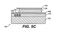
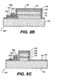
Figures 5A and 5B are schematic top views of the layer structure before and after, respectively, the second etching in fabricating the first embodiment. -
Figure 5C shows a cross-sectional view of the partially completed piezoelectric cantilever along theline 5C-5C inFigure 5B . -
Figure 6A is a schematic top view of the layer structure after the third etching in fabricating the first embodiment. -
Figure 6B shows a cross-sectional view of the partially completed piezoelectric cantilever along theline 6B-6B inFigure 6A . -
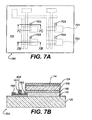
Figure 7A is a schematic top view of the layer structure after the fourth etching in fabricating the first embodiment. -
Figures 7B and7C show cross-sectional views of the partially completed piezoelectric cantilever along thelines 7B-7B and 7C-7C inFigure 7A . -
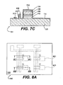
Figure 8A is a schematic top view of the layer structure after depositing the X-line metal layer in fabricating the first embodiment. -
Figures 8B and 8C show cross-sectional views of the partially completed piezoelectric cantilever along thelines 8B-8B and 8C-8C inFigure 8A . -
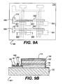
Figure 9A is a schematic top view of the layer structure after the fifth etching in fabricating the first embodiment. -
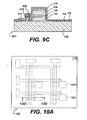
Figures 9B and9C are cross-sectional views of the partially completed piezoelectric cantilever along thelines 9B-9B and 9C-9C inFigure 9A . -
Figure 10A is a schematic top view of the layer structure after formation of the second protective coating in fabricating the first embodiment. -
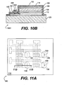
Figure 10B shows a cross-sectional view of the partially completed piezoelectric cantilever along theline 10B-10B inFigure 10A . -
Figure 11A is a schematic top view of the layer structure after the sixth etching in fabricating the first embodiment. -
Figure 11B shows a cross-sectional view of the piezoelectric cantilever along theline 11B-11B inFigure 11A . -
Figure 12 is a schematic top view of the layer structure after the seventh etching in fabricating the first embodiment. -
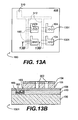
Figures 13A is a schematic top view of the layer structure inFigure 4D after the second etching in fabricating the second embodiment. -
Figure 13B is a schematic cross-sectional view of the partially completed piezoelectric cantilever along theline 13B-13B inFigure 13A . -
Figure 14A is a schematic top view of the layer structure after the third etching in fabricating the second embodiment. -
Figure 14B is a schematic cross-sectional view of the partially completed piezoelectric cantilever along theline 14B-14B inFigure 14A . -
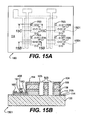
Figure 15A is a schematic top view of the layer structure after the fourth etching in fabricating the second embodiment. -
Figures 15B and15C are schematic cross-sectional views of the partially completed piezoelectric cantilever along thelines 15B-15B and 15C-15C inFigure 15A . -
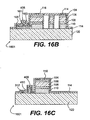
Figure 16A is a schematic top view of the layer structure after depositing the X-line metal layer in fabricating the second embodiment. -
Figures 16B and 16C are schematic cross-sectional views of the partially completed piezoelectric cantilever along thelines 16B-16B and 16C-16C inFigure 16A . -
Figure 17A is a schematic top view of the layer structure after the fifth etching in fabricating the second embodiment. -
Figures 17B and17C are schematic cross-sectional views of the partially completed piezoelectric cantilever along thelines 17B-17B and 17C-17C inFigure 17A . -
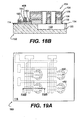
Figure 18A is a schematic top view of the layer structure after the sixth etching in fabricating the second embodiment. -
Figure 18B is a schematic cross-sectional view of the completed piezoelectric cantilever along theline 18B-18B inFigure 18A . -
Figure 19A is a schematic top view of a layer structure after the formation of the second protective coating in fabricating the second embodiment. -
Figure 19B is a schematic cross-sectional view of the completed piezoelectric cantilever along theline 19B-19B inFigure 19A . -
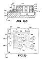
Figure 20 is a schematic top view of the layer structure after the seventh etching in fabricating the second embodiment. -
Figures 21A-21K are schematic cross-sectional views depicting a second layer structure at different stages of its manufacture in fabricating the third embodiment. -
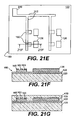
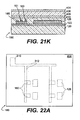
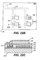
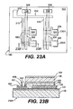
Figures 22A and22B are schematic top views of the layer structure before and after the third etching, respectively, in fabricating the third embodiment. -
Figure 22C is a schematic cross-sectional view of the partially completed piezoelectric cantilever along theline 22C-22C inFigure 22B . -
Figure 23A is a schematic top view of the layer structure after the fourth etching in fabricating the third embodiment. -
Figure 23B is a schematic cross-sectional view of the partially completed piezoelectric cantilever along theline 23B-23B inFigure 23A . -
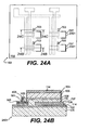
Figure 24A is a schematic top view of the layer structure after the fifth etching in fabricating the third embodiment. -
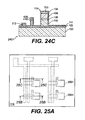
Figures 24B and24C are schematic cross-sectional views of the partially completed piezoelectric cantilever along thelines 24B-24B and 24C-24C inFigure 24A . -
Figure 25A is a schematic top view of the layer structure after the deposition of the X-line metal layer in fabricating the third embodiment. -
Figures 25B and 25C are schematic cross-sectional views of the partially completed piezoelectric cantilever along thelines 25B-25B and 25C-25C inFigure 25A . -
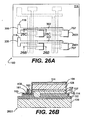
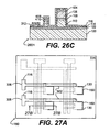
Figure 26A is a schematic top view of the layer structure after the sixth etching in fabricating the third embodiment. -
Figures 26B and26C are schematic cross-sectional views of the partially completed piezoelectric cantilever along thelines 26B-26B and 26C-26C inFigure 26A . -
Figure 27A is a schematic top view of the layer structure after the seventh etching in fabricating the third embodiment. -
Figure 27B is a schematic cross-sectional view of a completed piezoelectric cantilever along theline 27B-27B inFigure 27A . -
Figure 28A is schematic top view of the layer structure after the formation of the second protective layer in fabricating the third embodiment. -
Figure 28B is a schematic cross-sectional view of the completed piezoelectric cantilever along theline 28B-28B inFigure 28A . -
Figure 29 is a schematic top view of the layer structure after the eighth etching in fabricating the third embodiment. -
Figure 30 is a flow-chart of a process for manufacturing a piezoelectric cantilever pressure sensor array. -
Figure 1 shows a first embodiment of a piezoelectriccantilever pressure sensor 100 in its quiescent state. The piezoelectriccantilever pressure sensor 100 includes apiezoelectric cantilever 150 having abase portion 152 and abeam portion 154, and anaccess transistor 160 having agate contact 161, adrain contact 163, and asource contact 165. Thepiezoelectric cantilever 150 further includes, from top to bottom, atop electrode 104, apiezoelectric element 106, abottom electrode 108, and anelastic element 110. Theelectrodes piezoelectric element 106. Thebottom electrode 108 is also connected to thedrain contact 163 of theaccess transistor 160. Thebase portion 152 of thepiezoelectric cantilever 150 is supported by asubstrate 120, while thebeam portion 154 of thepiezoelectric cantilever 150 is suspended above acavity 130. - In this first embodiment, the
piezoelectric element 106 and theelastic element 110 form a asymmetrical piezoelectric bimorph, i.e., a two-layered structure having a piezoelectric element and a non-piezoelectric element. When the bimorph is bent, one element elongates and is under tensile stress while the other element contracts and is under compressive stress. In the quiescent, zero stress state of the piezoelectriccantilever pressure sensor 100, there is no voltage difference between theelectrodes cantilever pressure sensor 100, direct contact between a finger ridge and thebeam portion 154 of the piezoelectric cantilever 150 (shown as arrow A inFigure 1B ) will deflect thebeam portion 154 of thepiezoelectric cantilever 150. This causes tensile stress in thepiezoelectric element 106 and compressive stress in theelastic element 110. The stress in thepiezoelectric element 106 produces a proportional output voltage V between theelectrodes elastic element 110 offsets theneutral axis 140 of stress in thepiezoelectric cantilever 150 so that strain produced by piezoelectric effect is translated into an output voltage in thepiezoelectric element 106. Typically, the piezoelectriccantilever pressure sensor 100 is capable of generating a voltage in the range of 100 mV to 1.0 V with a typical finger touch. A detailed description on the mathematical modeling of thepiezoelectric cantilever 150 can be found, for example, in "Modeling and Optimal Design of Piezoelectric Cantilever Microactuators" (DeVoe and Pisano, IEEE J. Microelectromech. Syst., 6:266-270, 1997). - The material of
substrate 120 is any etchable material. The material ofsubstrate 120 is additionally selected based on its thermal stability, chemical inertness, specific coefficients of thermal expansion, and cost. In one embodiment, the material of the substrate is glass. Examples of glasses include, but are not limited to, borosilicate glasses, ceramic glasses, quartz and fused silica glasses, and soda lime glasses. The thickness of thesubstrate 120 may vary depending on the substrate material and the manufacturing process. In an embodiment, the material of thesubstrate 120 is a borosilicate glass and the substrate has a thickness of about 0.5 mm to about 1 mm. In this disclosure, the major surface of thesubstrate 120 on which thepiezoelectric cantilever 150 is located will be called the top surface of the substrate and the major surface of the substrate opposite the top surface will be called the bottom surface. - The material of the
piezoelectric element 106 is a piezoelectric material. Examples of the piezoelectric material include, but are not limited to, lead zirconate titanate (PZT), lead magnesium niobate-lead zirconate titanate (PMN-PZT), lead zirconate niobate-lead zirconate titanate (PZN-PZT), aluminum nitride (A1N), and zinc oxide (ZnO). The thickness of thepiezoelectric element 106 depends on the piezoelectric material and the specific requirement of a particular application. In an embodiment, thepiezoelectric element 106 has a thickness of about 0.5 µm to about 1 µm and is composed of PZT with a zirconium/titanium molar ratio of about 0.4 to about 0.6. - The
electrodes electrodes top electrode 104 is composed of platinum and thebottom electrode 108 is composed of a layer of platinum and a layer of titanium or titanium oxide (TiOx). - The
elastic element 110 is typically composed of a silicon-based material. Examples include, but are not limited to, silicon, polycrystalline silicon (polysilicon), and silicon nitride (SiNx). The thickness of theelastic element 110 is typically in the range of 0.2-1 µm. In an embodiment, theelastic element 110 is composed of silicon or silicon nitride and has a thickness of about 0.3-0.7 µm. - In all the embodiments described herein, the beam portion of the piezoelectric cantilever, e.g., the
beam portion 154 of thepiezoelectric cantilever 150, is designed to have a rigidity that would allow a deflection large enough to generate a measurable voltage under the pressure from a finger. Typically, the load applied by an individual's finger on a fingerprint sensor surface is in the range of 100-500 g. A fingerprint sensor surface is approximately 15 mm x 15 mm in dimensions. Assuming the fingerprint sensor has an array of piezoelectric cantilever pressure sensors with a standard pitch (i.e., distance between two neighboring sensors) of 50 µm, which corresponds to at least 500 dot per inch (dpi) specified by the Federal Bureau of Investigation, there will be a total of 90,000 sensors in the fingerprint area. As a first order approximation, one can assume that the area of the fingerprint ridges is equal to that of the fingerprint valleys. Accordingly, approximately 45,000 sensors will bear the applied load from the fingerprint. If one conservatively assumes an applied load of 90 grams from the fingerprint, then eachbeam portion 154 of thepiezoelectric cantilever 150 bears a load of about 2 mg. Since the beam needs to fit within the array pitch dimensions of a maximum of 50 µm x 50 µm, the length and width of thebeam portion 154 of thepiezoelectric cantilever 150 need to be less than the array pitch. Based on the length, width, thickness, and Young's Modulus for the beam material, the possible deflection of thebeam portion 154 of thepiezoelectric cantilever 150 under a given load and the voltage generated by the deflection can be determined. In an embodiment, thepiezoelectric cantilever 150 is capable of producing a maximum voltage in the range of 500-1,000 mV under normal pressure from a finger. - The
cavity 130 under thepiezoelectric cantilever 150 is deep enough to allow maximum deflection of thecantilever 150. In the first embodiment shown inFigures 1A and 1B , thecavity 130 extends through the thickness of thesubstrate 120 and is formed by etching from the bottom surface of thesubstrate 120. -
Figure 1C shows a second embodiment of piezoelectriccantilever pressure sensor 100 in which thecavity 130 extends into thesubstrate 120 from the top surface of the substrate. Typically, thecavity 130 does not extend all the way to the bottom surface of thesubstrate 120 in this embodiment. In this embodiment, releasingholes 503 extend through the thickness of thebeam portion 154 of the piezoelectric cantilever. The releasing holes permit etching of thecavity 130 from the top surface of the substrate to release thebeam portion 154 of the piezoelectric cantilever from the substrate. -
Figure 1D shows a third embodiment of piezoelectriccantilever pressure sensor 100 in which theelastic element 110 is shaped to define apedestal 111 that spaces the substrate-facing surface of thebeam portion 154 of thepiezoelectric cantilever 150 from the major surface of thesubstrate 120. In this embodiment, thecavity 130 is located between the substrate-facing surface of thebeam portion 154 and the top surface of thesubstrate 120. The elastic element is shaped with the aid of a sacrificial mesa, as will be described in detail below. - The second and third embodiments shown in
Figures 1C and1D are otherwise similar to the first embodiment shown inFigure 1A and 1B , and will not be described further here. Exemplary methods that can be used to fabricate all three embodiments will be described below. -
Figure 2 shows a fourth embodiment of a piezoelectriccantilever pressure sensor 200 in which the piezoelectric cantilever incorporates a symmetrical piezoelectric bimorph. Piezoelectriccantilever pressure sensor 200 is based on the first embodiment of the piezoelectric cantilever pressure sensor described above with reference toFigures 1A and 1B . The second and third embodiments of the piezoelectric cantilever pressure sensor described above with reference toFigures 1C and1D , respectively, may be similarly modified to incorporate a symmetrical piezoelectric bimorph. - The piezoelectric
cantilever pressure sensor 200 includes apiezoelectric cantilever 250 having abase portion 252 and abeam portion 254, and theaccess transistor 160 having thegate contact 161, thedrain contact 163, and thesource contact 165. Thepiezoelectric cantilever 250 incorporates a symmetrical piezoelectric bimorph composed of, from top to bottom, thetop electrode 104, thepiezoelectric element 106, amiddle electrode 112, an additionalpiezoelectric element 107, and thebottom electrode 108, all of which are supported by thesubstrate 120. Theelectrodes piezoelectric element 106. Theelectrodes piezoelectric element 107. Thebottom electrode 108 is connected to thedrain contact 163 of theaccess transistor 160. - In this fourth embodiment, the
piezoelectric elements piezoelectric element 106 elongates and is under tensile stress while thepiezoelectric element 107 contracts and is under compressive stress. -
Figure 3A shows a highly simplified example of a piezoelectric cantileverpressure sensor array 300 composed of four piezoelectric cantilever pressure sensors in a two-by-two matrix. In the example shown, the piezoelectric cantilever pressure sensors are the first embodiment of the piezoelectriccantilever pressure sensors 100 described above with reference toFigures 1A and 1B . However, the piezoelectric cantileverpressure sensor array 300 can incorporate any of the above-described piezoelectric cantilever pressure sensor embodiments. The piezoelectriccantilever pressure sensors 100 are connected to a grid of X-axis contact lines (X-lines) 302 and Y-axis contact lines (Y-lines) 304. Eachline cantilever pressure sensors 100 in each row of the array are connected to a respective X-line and the gates of theaccess transistors 160 of the piezoelectriccantilever pressure sensors 100 in each column of the array are connected to a respective Y-line. Additionally, the sources of theaccess transistors 160 of the piezoelectriccantilever pressure sensors 100 in each column of the array are connected to a respective reference voltage contact line (reference line) 312. The reference lines 312 are connected to an exposed reference voltage contact pad (reference pad) 310. Typically, the piezoelectric cantileverpressure sensor array 300 has a pitch of 50 µm and an array size of 300 x 300 or 256 x 360. - The state of each piezoelectric
cantilever pressure sensor 100 in the piezoelectric cantileverpressure sensor array 300 is read out by theaccess transistor 160 connected to thepiezoelectric cantilever 150 and typically located adjacent thebase portion 152 of eachpiezoelectric cantilever 150 as shown inFigure 1A . As shown inFigures 3B and 3C , thegate contact 161 of theaccess transistor 160 is connected to the Y-line, thedrain contact 163 of theaccess transistor 160 is connected to thebottom electrode 108 of thepiezoelectric cantilever 150, and the source contact 165 of theaccess transistor 160 is connected to a reference voltage Vref by thereference line 312 shown inFigure 3A . Thepiezoelectric cantilever 150 is accessed through theaccess transistor 160 by providing an activation signal on the Y-line and detecting the voltage signal output by thepiezoelectric cantilever 150 on the X-line. The access signal causes theaccess transistor 160 to connect thebottom electrode 108 to the reference voltage, typically ground, applied to thereference pad 310. Thepiezoelectric cantilever 150 bent by a fingerprint ridge will be said to be in an on state. Apiezoelectric cantilever 150 in the on state delivers the output signal, typically in the range of 500-1000 mV, to the X-line (Figure 3B ), when the piezoelectriccantilever pressure sensor 100 is accessed through itsaccess transistor 160 by the activation signal. On the other hand, thepiezoelectric cantilever 150 under a fingerprint valley is not bent and will be said to be in an off state. Apiezoelectric cantilever 150 in the off state generates no voltage difference between theelectrodes cantilever pressure sensor 100 is accessed through itsaccess transistor 160 by the activation signal, no output signal is generated on the X-line (Figure 3C ). A typical capacitance of the piezoelectriccantilever pressure sensor 100 is from 0.5 to 2 pF. The parasitic capacitance of the X-line is typically in the range of 1 to 5 pF and the sensing current in the X-line is in the order of 1-10 µA. The resistance of the X-line is in the order of few hundred Ohms, which results in a very fast operation of the piezoelectriccantilever pressure sensor 100. -
Figure 3D shows acircuit 400 that serves to record the status of the sensors of the piezoelectric cantileverpressure sensor array 300. Each piezoelectriccantilever pressure sensor 100 in thecircuit 400 has a unique X-Y address based on its position in the X-line/Y-line matrix. The read-outcircuits 170 scan the matrix by sequentially sending out activation signals to Y-lines. The status of each piezoelectriccantilever pressure sensor 100 is determined on the X-line to which it is connected based on its response to the activation signal. Typically, to distinguish between a real signal and an aberrant voltage fluctuation, the scan is repeated hundreds of times each second. Only signals detected for two or more scans are acted upon by the read-outcircuits 170. Such read-out circuits and the scanning mechanism are known in the art. - In addition to fingerprint detection, the piezoelectric cantilever
pressure sensor array 300 has utility in many other applications. The piezoelectric cantileverpressure sensor array 300 may be used for tactile imaging of lumps in soft tissue in medical devices. For example, the piezoelectric cantileverpressure sensor array 300 can be used in ultrasound imaging devices to provide a three-dimensional image of breast cancer or as an electric "fingertip" in remote surgery. The piezoelectric cantileverpressure sensor array 300 may also be used to detect nano- or micro-movement. For example, the piezoelectric cantileverpressure sensor array 300 can be used in automobile electronics as a tire pressure sensor or an impact sensor and in microphones and micro-speakers as an acoustic sensor. The piezoelectric cantilever sensors can also be used as microactuators or nanopositioners by applying a drive voltage to them. -
Figures 4A-4F ,5A-5C ,6A, 6B ,7A-7C ,8A-8C ,9A-9C ,10A, 10B ,11A, 11B , and12 illustrate a first embodiment of a method of making an array of piezoelectric cantilever pressure sensors that incorporates piezoelectriccantilever pressure sensors 100 in accordance with the first embodiment described above with reference toFigures 1A and 1B . The piezoelectric cantilever sensor array made by the method is otherwise similar to thearray 300 described above with reference toFigures 3A and3D . - The first embodiment of the method starts with the fabrication of a layer structure that can also be used in a second embodiment of the method, to be described below. The second embodiment of the method is for making an array of piezoelectric cantilever pressure sensors that incorporates piezoelectric
cantilever pressure sensors 100 in accordance with the second embodiment shown inFigure 1C . -
Figures 4A-4F show the fabrication of alayer structure 180 by mountingprefabricated access transistors 160 on the top surface of the substrate 120 (Figure 4A ); forming the reference pad 310 (Figure 3A ) and reference lines 312 (Figure 3A ) connecting the reference pad (not shown inFigure 4A ) to thesource contacts 165 of the access transistors; depositing theelastic layer 410 on the substrate 120 (Figure 4B ); formingcontact holes elastic layer 410 to thegate contact 161 anddrain contact 163, respectively, of each access transistor 160 (Figure 4C ); depositing abottom electrode layer 408 on the elastic layer 410 (Figure 4D ); depositing apiezoelectric layer 406 on the bottom electrode layer 408 (Figure 4E ); and depositing atop electrode layer 404 on the piezoelectric layer 106 (Figure 4F ). - The
elastic layer 410, the electrode layers 408 and 404, and thepiezoelectric layer 406 are deposited by a process such as sputtering, chemical vapor deposition (CVD), plasma CVD, physical vapor deposition (PVD) or the like. The contact holes 171 and 173 are formed by a first etching process that uses a first mask. Thelayer structure 180 fabricated as just described is shown inFigure 4F . Thelayer structure 180 is then subject to additional processing to form the array of piezoelectric cantilever pressure sensors. - As described above, the thickness of each layer of the
layer structure 180 depends on the specific requirements of a particular application. Either or both of the electrode layers 404 and 408 may also be a layer structure. In one embodiment, thesubstrate 120 is composed of borosilicate glass with a thickness of about 0.5 mm; theelastic layer 410 is composed of silicon nitride with a thickness of about 500 nm; thebottom electrode layer 408 has a two-layered structure composed of a platinum layer with a thickness of about 100 nm and a titanium oxide layer with a thickness of about 50 nm; thepiezoelectric layer 406 has a thickness of about 500 nm to about 1,000 nm and is composed of PZT with a zirconium/titanium ratio of 0.4 to 0.6; thetop electrode layer 404 has a thickness of about 100 nm and is composed of platinum. - Next, as shown in
Figures 5A-5C , thelayer structure 180 is subject to a second etching process that uses a second mask.Figure 5A shows thelayer structure 180 before the second etching process is performed. The locations on the surface of the substrate of theaccess transistors 160, thereference lines 312 and thereference pad 310 are shown by broken lines. The second etching process defines partially completedpiezoelectric cantilevers 501 in thetop electrode layer 404 and thepiezoelectric layer 406. In an embodiment, the partially completedpiezoelectric cantilever 501 has dimensions of 25 µm x 10 µm (top view) to conform to the standard sensor pitch of 50 µm. As shown inFigures 5B and5C , the second etching process removes part of thetop electrode layer 404 and thepiezoelectric layer 406 to define thetop electrode 104 and thepiezoelectric element 106 of the partially completed piezoelectric cantilevers in these layers, and additionally exposes part of thebottom electrode layer 408 for the next etching process. - After the second etching process, the
layer structure 180 is subject to a third etching process that uses a third mask. As shown inFigures 6A and 6B , the third etching process removes the unmasked portion of thebottom electrode layer 408 to define thebottom electrodes 108, the Y-lines 304 and Y-pads 308, and the electrical connection between the bottom electrodes and the drains of therespective access transistors 160. The third etching process additionally removes the unmasked portion of theelastic layer 410 to define theelastic element 110 and to expose theaccess transistors 160, theprefabricated reference pad 310 and thereference lines 312, which are connected to thesource contacts 165 of theaccess transistors 160. The Y-lines 304 are connected to thegate contacts 161 of theaccess transistors 160. One of the Y-lines is shown as part of thebottom metal layer 408 on thegate contact 161 inFigure 6B . The third etching process forms partially completedpiezoelectric cantilevers 601. - Next, the
layer structure 180 is coated with a firstprotective layer 114, as shown inFigures 7A and 7B , followed by a fourth etching process that uses a fourth mask. Theprotective layer 114 prevents hydrogen or water penetration. Theprotective layer 114 is composed of aluminum oxide or any other suitable material. Theprotective layer 114 is deposited by a process such as sputtering, CVD, plasma CVD, PVD or the like. The fourth etching process formscontact openings 703 in theprotective layer 114. As shown inFigures 7A and7C , the contact openings expose part of thetop electrodes 104 of the partially completedpiezoelectric cantilevers 601. - After the fourth etching process, an
X-line metal layer 116 is deposited on the firstprotective layer 114, as shown inFigures 8A and8B . TheX-line metal layer 116 is deposited by a process such as sputtering, CVD, plasma CVD, PVD or the like. TheX-line metal layer 116 is typically composed of aluminum or an aluminum alloy. As shown inFigure 8C , theX-line metal layer 116 fills thecontact opening 703 in the firstprotective layer 114 and is thus electrically connected to thetop electrode 104 of the partially completedpiezoelectric cantilever 801. - Next, a fifth etching process that uses a fifth mask is performed to define the X-lines 302 and X-pads 306 in the
X-line metal layer 116. As shown inFigures 9A-9C , the fifth etching process removes the unmasked portion of theX-line metal layer 116 to define the X-lines 302 and the X-pads 306 and additionally exposes the firstprotective layer 114. - After the fifth etching process, a second
protective layer 118 is deposited on thelayer structure 180 by spin coating, as shown inFigures 10A and10B . The second protective layer prevents direct contact between the fingertip and theX-lines 302. The secondprotective layer 118 is composed of any material that meets the heat resistance, chemical resistance, and insulation requirement. The secondprotective layer 118 is also flexible enough to allow repeated deformation. In one embodiment, the secondprotective layer 118 is composed of polyimide and has a thickness of about 2-7 µm. - After the second
protective layer 118 is deposited, thelayer structure 180 is subject to a sixth etching process that uses a sixth mask. The sixth etching process is performed by applying the etchant to the bottom surface of thesubstrate 120. The sixth etching process forms acavity 130 that extends through thesubstrate 120 to theelastic element 110 of each completedpiezoelectric cantilever 150, as shown inFigures 11A and11B . Forming thecavity 130 releases thebeam portion 154 of eachpiezoelectric cantilever 150 from the substrate to complete the fabrication of the piezoelectric cantilevers. - Next, a seventh and final etching process that uses a seventh mask is performed. The seventh etching process removes portions of the first
protective layer 114 and the secondprotective layer 118 to expose the X-pads 306, the Y-pads 308, and thereference pad 310, as shown inFigure 12 . - The method just described fabricates a piezoelectric cantilever
pressure sensor array 300 with piezoelectriccantilever pressure sensors 100 in accordance with the first embodiment connected to theX-lines 302, the Y-lines 304, and thereference lines 312, as shown inFigure 12 . As is known in the art, thepiezoelectric cantilevers 150, the X-lines 302 and X-pads 306, the Y-lines 304 and Y-pads 308, thereference lines 312 andreference pad 310, and thecavities 130 may differ in size, shape and layout from the example shown in the figures. For example, the shape of thecavities 130 can be round, oval, or rectangular. - Alternatively, the
access transistors 160 can be fabricated after thepiezoelectric cantilevers 150 have been defined in thelayer structure 180 and thecavities 130 have been etched. Thedrain contacts 163 of theaccess transistors 160 are connected to thebottom electrodes 108 of thepiezoelectric cantilevers 150 by a metallization process. Thereference pad 310 andreference lines 312 are fabricated and connected to thegate contact 161 of theaccess transistor 160 by the same or another metallization process. The fabrication process foraccess transistors 160 is known in the art. For example, the process is described in detail in the book, "Thin Film Transistors" by C.R. Kagan and P. Andry, Marcel Dekker (New York, 2003), which is hereby incorporated by reference. -
Figures 13A, 13B ,14A, 14B ,15A-15C ,16A-16C ,17A-17C ,18A, 18B ,19A, 19B , and20 illustrate the above-mentioned second embodiment of a method of making an array of piezoelectric cantilever pressure sensors that incorporates piezoelectriccantilever pressure sensors 100 in accordance with the second embodiment described above with reference toFigure 1C . The piezoelectric cantilever sensor array is otherwise similar to thearray 300 described above with reference toFigures 3A and3D . This second embodiment of the method fabricates the piezoelectric cantilever pressure sensor array using thelayer structure 180 whose fabrication is described above with reference toFigures 4A-4F . - This second embodiment begins with the fabrication of the
layer structure 180 as described above with reference toFigures 4A-4F . Thelayer structure 180 is then subject to a second etching process that uses a second mask. The second mask is similar to that used in the second etching process described above with reference toFigures 5A-5C except that it additionally defines releasingholes 503 in thebeam portion 154 of each partially completedpiezoelectric cantilever 1301. The releasing holes are used later to facilitate etching part of the cavity under each beam portion. - As shown in
Figure 13B , the second etching process removes part of thetop electrode layer 404 and thepiezoelectric layer 406 to define thetop electrode 104 and thepiezoelectric element 106 of the partially completedpiezoelectric cantilevers 1301 and to define the releasingholes 503 that extend through the top electrode layer and the piezoelectric layer. The second etching process additionally exposes part of thebottom electrode layer 408 for the next etching process. - After the second etching process, the
layer structure 180 is subject to a third etching process that uses a third mask. As shown inFigures 14A and 14B , the third etching process removes the unmasked portion of thebottom electrode layer 408 to define thebottom electrodes 108, the Y-lines 304 and Y-pads 308 and the electrical connection between the bottom electrodes and the drains of therespective access transistors 160. The third etching process additionally removes the unmasked portion of theelastic layer 410 to define theelastic element 110 and to expose theprefabricated reference pad 310 andreference lines 312, which are connected to thesource contacts 165 of theaccess transistors 160. The Y-lines 304 are connected to thegate contacts 161 of theaccess transistors 160. One of the Y-lines 304 is shown as part of thebottom electrode layer 408 on thegate contact 161 inFigure 14B . The third etching process forms a partially completedpiezoelectric cantilever 1401. - Next, the
layer structure 180 is coated with a firstprotective layer 114, as shown inFigures 15A and 15B , followed by a fourth etching process that uses a fourth mask. Theprotective layer 114 prevents hydrogen or water penetration. Theprotective layer 114 is composed of aluminum oxide or any other suitable material. Theprotective layer 114 is deposited by a process such as sputtering, CVD, plasma CVD, PVD or the like. - The fourth etching process forms in the
protective layer 114contact openings 703 and additionally forms a second set of releasingholes 705 around each partially completedpiezoelectric cantilever 1501. The fourth etching process also re-opens the releasingholes 503 that extend through thebeam portion 154 of each partially completedpiezoelectric cantilever 1501. As shown inFigures 15A-15C , thecontact openings 703 expose thetop electrode layer 104, while the releasingholes substrate 120. Theinterior wall 505 of the releasingholes 503 remains covered by theprotective coating layer 114 after the fourth etching process. - Next, an
X-line metal layer 116 is deposited on the firstprotective layer 114, as shown inFigures 16A and16B . Themetal layer 116 is deposited by a process such as sputtering, CVD, plasma CVD, PVD or the like. TheX-line metal layer 116 is typically composed of aluminum or an aluminum alloy. As shown inFigure 16C , theX-line metal layer 116 fills thecontact opening 703 in the firstprotective layer 114 and is thus electrically connected to thetop electrode 104 of the partially completedpiezoelectric cantilever 1601. - Next, a fifth etching process that uses a fifth mask is performed to define the X-lines 302 and X-pads 306 in the
X-line metal layer 116. As shown inFigures 17A-17C , the fifth etching process removes the unmasked portion of theX-line metal layer 116 to define the X-lines and X-pads and exposes the firstprotective layer 114. The fifth etching process additionally re-opens the releasingholes Figure 17B . - After the fifth etching process, the
layer structure 180 is subject to a sixth etching process that creates acavity 130 under thebeam portion 154 of eachpiezoelectric cantilever 150, as shown inFigures 18A and18B . The sixth etching process releases thebeam portions 154 from the surface of thesubstrate 120. No mask is needed for this etching process. Etchant flows through the releasingholes Figure 18B to the portion of the top surface of thesubstrate 120 under theelastic element 110 and etches away this portion of the substrate to form thecavity 130. Typically, the sixth etching process etches thecavity 130 to a depth that is larger than the maximum possible deflection of thepiezoelectric cantilever 150 under the pressure from a fingertip, but is substantially less than the total thickness of thesubstrate 120. Consequently, the sixth etching process is substantially shorter in duration than the etching process performed from the bottom surface of the substrate to form the cavity in the first embodiment of the method described above. - After the sixth etching process, a second
protective layer 118 is deposited on thelayer structure 180 by spin coating, as shown inFigures 19A and19B . The second protective layer prevents direct contact between the fingertip and theX-lines 302. - Finally, after the second
protective layer 118 has been deposited, a seventh etching process that uses a seventh mask is performed. The seventh etching process removes portions of the firstprotective layer 114 and the secondprotective layer 118 to expose the X-pads 306, the Y-pads 308, and thereference pad 310, as shown inFigure 20 . - The method just described fabricates a piezoelectric cantilever
pressure sensor array 300 with piezoelectriccantilever pressure sensors 100 in accordance with the second embodiment connected to theX-lines 302, the Y-lines 304, and thereference lines 312, as shown inFigure 20 . As is known in the art, thepiezoelectric cantilevers 150, the X-lines 302 and X-pads 306, the Y-lines 304 and Y-pads 308, thereference lines 312 andreference pad 310, and thecavities 130 may differ in size, shape and layout from the example shown in the figures. -
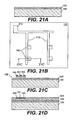
Figures 21A-21K ,22A-22C ,23A, 23B ,24A-24C ,25A-25C ,26A-26C ,27A, 27B ,28A, 28B and29 illustrate a third embodiment of a method of making a piezoelectric cantilever sensor array that incorporates piezoelectriccantilever pressure sensors 100 in accordance with the third embodiment described above with reference toFigure 1D . The piezoelectric cantilever sensor array made by the method is otherwise similar to thearray 300 described above with reference toFigures 3A and3D . - The third embodiment of the method starts with the fabrication of a
layer structure 180, as shown inFigures 21A-21K . Thelayer structure 180 is made by depositing thecoating layer 122 on the top surface of the substrate 120 (Figure 21A ); mountingprefabricated access transistors 160 on thecoating layer 122 and forming on thecoating layer 122 thereference pad 310 andreference lines 312 connecting thereference pad 310 to thesource contacts 165 of the access transistors 160 (Figures 21B and 21C ); depositing a sacrificial layer 426 typically of phosphosilicate glass (PSG) on the coating layer 122 (Figure 21D ); etching the sacrificial layer 426 using a first mask to define asacrificial mesa 126 adjacent each of theaccess transistors 160 and to expose theaccess transistors 160, thereference pad 310, thereference lines 312, and the coating layer 122 (Figures 21E and 21F ); depositing the elastic layer 410 (Figure 21G ); etching theelastic layer 410 using a second mask to createcontact holes elastic layer 410 to thegate contact 161 anddrain contact 163, respectively, of each access transistor 160 (Figure 21H ); depositing abottom electrode layer 408 on the elastic layer 410 (Figure 21I ); depositing apiezoelectric layer 406 on the bottom electrode layer 408 (Figure 21J ); and depositing atop electrode layer 404 on the piezoelectric layer 406 (Figure 21K ). Thecoating layer 122, sacrificial layer 124,elastic layer 410, electrode layers 408 and 404, and thepiezoelectric layer 406 are deposited by a process such as sputtering, chemical vapor deposition (CVD), plasma CVD, physical vapor deposition (PVD) or the like. Thelayer structure 180 fabricated as just described is shown inFigure 21K . As will be described in the following paragraphs, thesacrificial mesas 126 will be etched away to form a cavity under thebeam portion 154 of eachpiezoelectric cantilever 150. Accordingly, thesacrificial mesas 126 typically have dimensions that are slightly larger than the dimensions of thebeam portion 154 of thepiezoelectric cantilever 150, as shown inFigure 5B . The thickness of thesacrificial mesas 126 is typically larger than the maximum possible deflection of thebeam portion 154 of thepiezoelectric cantilever 150. In other words, the cavity created by etching away thesacrificial mesa 126 typically has a depth that accommodates the maximum possible deflection of thebeam portion 154 of thepiezoelectric cantilever 150. - Next, as shown in
Figures 22A-22C , thelayer structure 180 is subject to a third etching process that uses a third mask. The third etching process partially define the piezoelectric cantilevers in thetop electrode layer 404 and thepiezoelectric layer 406.Figure 22A shows thelayer structure 180 before the second etching process is performed. The locations on the surface of the substrate of theaccess transistors 160, thereference lines 312, thereference pad 310, and thesacrificial mesas 126 are shown by broken lines. The third etching process defines partially completedpiezoelectric cantilevers 2201 in thetop electrode layer 404 and thepiezoelectric layer 406. As shown inFigures 22B and 22C , the third etching process removes part of thetop electrode layer 404 and thepiezoelectric layer 406 to define thetop electrode 104 and thepiezoelectric element 106 of the partially completed piezoelectric cantilevers in these layers, and additionally exposes part of thebottom electrode layer 408 for the next etching process. - After the third etching process, the
layer structure 180 is subject to a fourth etching process that uses a fourth mask. As shown inFigures 23A and 23B , the fourth etching process removes the unmasked portion of thebottom electrode layer 408 to define thebottom electrodes 108, the Y-lines 304 and Y-pads 308, and the electrical connection between the bottom electrodes and the drains of therespective access transistors 160. The fourth etching process additionally removes the unmasked portion of theelastic layer 410 to define theelastic element 110 and to expose theaccess transistors 160, part of thesacrificial mesas 126, theprefabricated reference pad 310 andreference lines 312. The part of theelastic element 110 that later becomes part of the beam portion of the completed piezoelectric cantilever extends over thesacrificial mesa 126. The reference lines are connected to thesource contacts 165 of theaccess transistors 160. The Y-lines 304 are electrically connected to thegate contact 161 of theaccess transistors 160 in each column. One of the Y-lines is shown as part of thebottom electrode layer 408 on thegate contact 161 inFigure 23B . The fourth etching process forms partially completedpiezoelectric cantilevers 2301. - Next, the
layer structure 180 is coated with a firstprotective layer 114, as shown inFigures 24A and 24B , followed by a fifth etching process that uses a fifth mask. Theprotective layer 114 prevents hydrogen or water penetration. Theprotective layer 114 is composed of aluminum oxide or any other suitable material. Theprotective layer 114 is deposited by a process such as sputtering, CVD, plasma CVD, PVD or the like. The fifth etching process formscontact openings 703 in theprotective layer 114 on each partially completedpiezoelectric cantilever 2401. The fifth etching process additionally formsrelease openings 707 around each partially completedpiezoelectric cantilever 2401, as shown inFigure 24B . As shown inFigures 24B and24C , therelease openings 707 expose part of thesacrificial mesas 126 and thecontact openings 703 expose thetop electrodes 104. - After the fifth etching process, an
X-line metal layer 116 is deposited on the firstprotective layer 114, as shown inFigures 25A and25B . The X-line metal layer is deposited by a process such as sputtering, CVD, plasma CVD, PVD or the like. TheX-line metal layer 116 is typically composed of aluminum or an aluminum alloy. As shown inFigure 25C , theX-line metal layer 116 fills thecontact opening 703 in the firstprotective layer 114 and is thus electrically connected to thetop electrode 104 of the partially completedpiezoelectric cantilever 2501. - Next, a sixth etching process that uses a sixth mask is performed to define the X-lines 302 and X-pads 306 in the
X-line metal layer 116. The sixth etching process additionally reopens therelease openings 707. As shown inFigures 26A-26C , the sixth etching process removes the unmasked portion of theX-line metal layer 116 to define the X-lines 302 and X-pads 306, and additionally exposes the firstprotective layer 114 and re-opens therelease openings 707 to expose part of thesacrificial mesas 126. - After the sixth etching process, a seventh etching process is performed to create the
cavities 130 by removing thesacrificial mesas 126, as shown inFigures 27A and27B . No mask is used in the seventh etching process. The etchant flows through therelease openings 707 and etches away thesacrificial mesa 126 from between the beam portion of eachpiezoelectric cantilever 150 and the top surface of theprotective layer 122. The seventh etching process releases thebeam portion 154 from thesubstrate 120. - Next, a second
protective layer 118 is deposited on thelayer structure 180 by spin coating, as shown inFigures 28A and28B . The second protective layer prevents direct contact between the fingertip and theX-lines 302. - Finally, an eighth and final etching process that uses a seventh mask is performed. The eighth etching process removes portions of the first
protective layer 114 and the secondprotective layer 118 to expose the X-pads 306, the Y-pads 308, and thereference pad 310, as shown inFigure 29 . - The third embodiment of the method just described fabricates a piezoelectric cantilever
pressure sensor array 300 with piezoelectriccantilever pressure sensors 100 in accordance with the third embodiment connected to theX-lines 302, the Y-lines 304, and thereference lines 312, as shown inFigure 29 . As is known in the art, thepiezoelectric cantilevers 150, the X-lines 302 and X-pads 306, the Y-lines 304 and Y-pads 308, thereference lines 312 andreference pad 310, and thecavities 130 may differ in size, shape and layout from the example shown in the figures. -
Figure 30 shows a method 3000 for manufacturing the piezoelectric cantileverpressure sensor array 300. In the method 3000, there is formed (3001) a layer structure having, in order, a substrate, an elastic layer, a bottom electrode layer, a piezoelectric layer, and a top electrode layer, piezoelectric cantilevers are defined (3003) in the layer structure, Y-lines and Y-pads are defined (3005) in the bottom electrode layer, X-lines and X-pads are formed (3007), and a cavity is created (3009) under each piezoelectric cantilever. - In an embodiment, the layer structure additionally has a prefabricated access transistor adjacent each piezoelectric cantilever. Defining the piezoelectric cantilever forming an electrical connection between the bottom electrode of the piezoelectric cantilever and the drain of the access transistor.
- In an embodiment, the cavity is created by etching the substrate from the bottom surface thereof. In another embodiment, the cavity is created by etching the substrate from the top surface thereof. In a third embodiment, the layer structure additionally has a sacrificial mesa and the piezoelectric cantilever partially overlaps the sacrificial mesa. In this embodiment, the cavity is created by removing the sacrificial mesa from under the piezoelectric cantilever.
- In yet another embodiment, the process of forming X-lines and X-pads includes forming a first protective coating, creating contact openings in the first protective coating, depositing an X-line metal layer on the first protective coating, and defining the X-lines and X-pads in the X-line metal layer. In another embodiment, the layer structure is covered by a flexible protective layer.
- Although preferred embodiments and their advantages have been described in detail, various changes, substitutions and alterations can be made herein without departing from the scope of the invention defined by the appended claims.
Claims (9)
- A piezoelectric cantilever pressure sensor (100), comprising:a substrate (120); andan elongate piezoelectric cantilever (150) mounted at one end on the substrate and extending over a cavity (130), the piezoelectric cantilever comprising:a first electrode (108);a second electrode (104);a piezoelectric element (106) between the first electrode and the second electrode and electrically connected thereto, andan access transistor,whereinthe access transistor comprises a source contact (165), a gate contact (161) and a drain contact (163);characterised in that the drain contact is connected to the first electrode;the source contact is connected to receive a reference voltage; andthe gate contact is connected to receive an activation signal.
- The piezoelectric cantilever pressure sensor of claim 1, additionally comprising
an access transistor (160) electrically connected to the piezoelectric cantilever. - The piezoelectric cantilever pressure sensor of one of claims 1 to 2, wherein
the piezoelectric cantilever additionally comprises an elastic element (110) between the piezoelectric element and the substrate. - The piezoelectric cantilever pressure sensor or claim 3, wherein the elastic layer comprises one of silicon and silicon nitride.
- The piezoelectric cantilever pressure sensor of claim 3 or 4, wherein:the substrate has a top surface on which the piezoelectric cantilever is located; andthe cavity is located between the elastic element and the top surface of the substrate.
- The piezoelectric cantilever pressure sensor of one of claims 1 to 5, wherein
the piezoelectric element comprises one of PZT, PMN-PZT, PZN-PZT, AIN and ZnO. - The piezoelectric cantilever pressure sensor of one of claims 1 to 6, wherein
at least one of the first electrode and the second electrode comprises one of gold, silver, platinum, palladium, copper, aluminum, and alloys thereof. - The piezoelectric cantilever pressure sensor of one of claims 1 to 7, wherein:the piezoelectric element (106) is a first piezoelectric element; andthe piezoelectric cantilever additionally comprises:a third electrode (112); anda second piezoelectric element (107) between the second electrode and the third electrode and electrically connected thereto.
- The piezoelectric cantilever pressure sensor of one of claims 1 to 8, wherein the substrate comprises glass.
Applications Claiming Priority (2)
| Application Number | Priority Date | Filing Date | Title |
|---|---|---|---|
| US792777 | 2004-03-05 | ||
| US10/792,777 US7104134B2 (en) | 2004-03-05 | 2004-03-05 | Piezoelectric cantilever pressure sensor |
Publications (2)
| Publication Number | Publication Date |
|---|---|
| EP1571435A1 EP1571435A1 (en) | 2005-09-07 |
| EP1571435B1 true EP1571435B1 (en) | 2009-05-20 |
Family
ID=34750612
Family Applications (1)
| Application Number | Title | Priority Date | Filing Date |
|---|---|---|---|
| EP04023608A Expired - Fee Related EP1571435B1 (en) | 2004-03-05 | 2004-10-04 | Piezoelectric cantilever pressure sensor |
Country Status (4)
| Country | Link |
|---|---|
| US (1) | US7104134B2 (en) |
| EP (1) | EP1571435B1 (en) |
| JP (1) | JP4832772B2 (en) |
| DE (1) | DE602004021168D1 (en) |
Families Citing this family (55)
| Publication number | Priority date | Publication date | Assignee | Title |
|---|---|---|---|---|
| US7497133B2 (en) | 2004-05-24 | 2009-03-03 | Drexel University | All electric piezoelectric finger sensor (PEFS) for soft material stiffness measurement |
| US8481335B2 (en) * | 2006-11-27 | 2013-07-09 | Drexel University | Specificity and sensitivity enhancement in cantilever sensing |
| US7992431B2 (en) | 2006-11-28 | 2011-08-09 | Drexel University | Piezoelectric microcantilevers and uses in atomic force microscopy |
| WO2008067386A2 (en) * | 2006-11-28 | 2008-06-05 | Drexel University | Piezoelectric microcantilever sensors for biosensing |
| US8110964B2 (en) * | 2007-01-29 | 2012-02-07 | Drexel University | Energy harvesting device |
| CA2677196A1 (en) * | 2007-02-01 | 2008-09-12 | Drexel University | A hand-held phase-shift detector for sensor applications |
| WO2008112713A1 (en) * | 2007-03-13 | 2008-09-18 | Nanoink, Inc. | Nanolithography with use of viewports |
| KR100914026B1 (en) | 2007-06-12 | 2009-08-28 | 한국세라믹기술원 | The Method for Manufacturing Fingerprint Sensor Using Piezoelectric Thin Film |
| KR100908124B1 (en) * | 2007-07-09 | 2009-07-16 | 삼성전자주식회사 | Pressure sensor for measuring blood pressure and manufacturing method thereof |
| WO2009079154A2 (en) * | 2007-11-23 | 2009-06-25 | Drexel University | Lead-free piezoelectric ceramic films and a method for making thereof |
| US8011237B2 (en) * | 2008-02-22 | 2011-09-06 | Hong Kong Applied Science And Technology Research Institute Co., Ltd. | Piezoelectric module for energy harvesting, such as in a tire pressure monitoring system |
| US8741663B2 (en) | 2008-03-11 | 2014-06-03 | Drexel University | Enhanced detection sensitivity with piezoelectric sensors |
| KR20110049748A (en) | 2008-05-16 | 2011-05-12 | 드렉셀유니버시티 | System and method for evaluating tissue |
| US10170685B2 (en) | 2008-06-30 | 2019-01-01 | The Regents Of The University Of Michigan | Piezoelectric MEMS microphone |
| EP3796671A1 (en) * | 2008-06-30 | 2021-03-24 | The Regents of the University of Michigan | Piezoelectric mems microphone |
| US8120232B2 (en) * | 2009-01-20 | 2012-02-21 | Palo Alto Research Center Incorporated | Sensors and actuators using piezo polymer layers |
| US8722427B2 (en) * | 2009-10-08 | 2014-05-13 | Drexel University | Determination of dissociation constants using piezoelectric microcantilevers |
| US20110086368A1 (en) * | 2009-10-08 | 2011-04-14 | Drexel University | Method for immune response detection |
| JP5463510B2 (en) * | 2010-06-22 | 2014-04-09 | 独立行政法人科学技術振興機構 | Physical quantity sensor and manufacturing method thereof |
| GB2494618B (en) * | 2011-08-22 | 2018-03-21 | Wheelright Ltd | Vehicle tyre pressure measurement |
| US8824706B2 (en) | 2011-08-30 | 2014-09-02 | Qualcomm Mems Technologies, Inc. | Piezoelectric microphone fabricated on glass |
| US8724832B2 (en) * | 2011-08-30 | 2014-05-13 | Qualcomm Mems Technologies, Inc. | Piezoelectric microphone fabricated on glass |
| JP5677258B2 (en) * | 2011-09-27 | 2015-02-25 | 株式会社東芝 | Strain detector and method of manufacturing the same |
| JP5807781B2 (en) * | 2011-12-26 | 2015-11-10 | アイシン精機株式会社 | Biological signal detector |
| JP5686443B2 (en) * | 2013-01-10 | 2015-03-18 | 日本写真印刷株式会社 | Film pressure sensor with adhesive layer, touch pad using the same, protection panel with touch input function, and electronic device |
| KR101453857B1 (en) | 2013-02-07 | 2014-10-22 | 한국기계연구원 | Pressure sensor and manufacturing method thereof |
| WO2015064217A1 (en) * | 2013-10-28 | 2015-05-07 | 株式会社村田製作所 | Piezoelectric sensor |
| EP3100020B1 (en) * | 2014-01-31 | 2019-01-02 | Nanotech Analysis S.r.l. | Miniaturized device for measurements of very low pressure and of gas concentrations |
| US10578508B2 (en) | 2014-01-31 | 2020-03-03 | Nanotech Analysis S.R.L. | Electro-mechanical miniaturized device for pressure measurements |
| JP6292932B2 (en) * | 2014-03-13 | 2018-03-14 | セイコーインスツル株式会社 | Pressure sensor |
| WO2016056419A1 (en) * | 2014-10-06 | 2016-04-14 | 国立大学法人東京大学 | Pressure sensor |
| DE102015224938B4 (en) | 2014-12-12 | 2021-09-23 | Leibniz-Institut für Festkörper- und Werkstoffforschung Dresden e.V. (IFW Dresden e.V.) | Method and device for determining force fields, force field gradients, material properties or masses with a system of coupled, vibratory, beam-like components |
| US9972723B2 (en) * | 2015-02-12 | 2018-05-15 | United Arab Emirates University | Piezoelectric thin-film based flexible sensing device, method for fabrication thereof and method for operating the same |
| TWI563253B (en) | 2015-04-14 | 2016-12-21 | Lee Mei Yen | Composite substrate sensor device and method of manufacturing such sensor device |
| CN106056033B (en) | 2015-04-14 | 2019-07-05 | 李美燕 | composite substrate sensing device and manufacturing method thereof |
| TWI574028B (en) * | 2015-06-22 | 2017-03-11 | 李美燕 | Integrated oscillating wave emitting and sensing member, sensing array and electronic apparatus using such member and method of manufacturing such member |
| EP3137964B1 (en) | 2015-06-26 | 2018-05-09 | SABIC Global Technologies B.V. | Integrated piezoelectric cantilever actuator and transistor for touch input and haptic feedback applications |
| US10062832B2 (en) | 2015-11-30 | 2018-08-28 | Sabic Global Technologies, B.V. | Methods and systems for making piezoelectric cantilever actuators |
| US9960715B1 (en) | 2016-03-22 | 2018-05-01 | The United States Of America, As Represented By The Secretary Of The Navy | Light activated piezoelectric converter |
| WO2017171855A1 (en) * | 2016-04-01 | 2017-10-05 | Intel Corporation | Strain sensitive piezoelectric system with optical indicator |
| CN105841850B (en) * | 2016-05-12 | 2018-02-27 | 京东方科技集团股份有限公司 | A kind of piezoelectric transducer and preparation method thereof |
| US10840430B2 (en) * | 2016-06-30 | 2020-11-17 | Intel Corporation | Piezoelectric package-integrated sensing devices |
| DE102016212717A1 (en) * | 2016-07-13 | 2018-01-18 | Robert Bosch Gmbh | Detection device for piezoelectric microphone |
| KR20180015482A (en) | 2016-08-03 | 2018-02-13 | 삼성전자주식회사 | Audio spectrum analyzer and method of arrangement of resonators included in the audio spectrum analyzer |
| CN106778691B (en) * | 2017-01-16 | 2020-04-21 | 业成科技(成都)有限公司 | Acoustic wave type fingerprint identification device, manufacturing method thereof and electronic device applying acoustic wave type fingerprint identification device |
| WO2018201853A1 (en) * | 2017-05-01 | 2018-11-08 | Shenzhen GOODIX Technology Co., Ltd. | Ultrasound fingerprint sensing and sensor fabrication |
| US10952642B2 (en) * | 2017-11-09 | 2021-03-23 | Amorepacific Corporation | Strain sensor unit and skin sensor module comprising the same |
| JP7027252B2 (en) | 2018-05-25 | 2022-03-01 | 株式会社東芝 | Vibration sensor and sensor module |
| TWI684367B (en) * | 2018-09-14 | 2020-02-01 | 美律實業股份有限公司 | Speaker and microelectromechanical actuator thereof |
| CN109734047B (en) * | 2019-02-27 | 2021-03-23 | 京东方科技集团股份有限公司 | MEMS device, manufacturing method thereof and display substrate |
| US11770657B2 (en) | 2019-08-06 | 2023-09-26 | Nisshinbo Micro Devices Inc. | Piezo-electric element |
| US11527700B2 (en) | 2019-12-20 | 2022-12-13 | Vanguard International Semiconductor Singapore Pte. Ltd. | Microphone device with single crystal piezoelectric film and method of forming the same |
| CN110943156B (en) * | 2019-12-24 | 2021-08-24 | 中山大学 | Pressure sensor based on piezoelectric material and preparation method |
| CN112968201B (en) * | 2021-02-05 | 2022-08-05 | 东莞市爱康智能技术有限公司 | Self-adaptive hot pressing mechanism |
| KR20230024872A (en) * | 2021-08-11 | 2023-02-21 | 썬전 샥 컴퍼니 리미티드 | microphone |
Family Cites Families (17)
| Publication number | Priority date | Publication date | Assignee | Title |
|---|---|---|---|---|
| JPH07121159B2 (en) * | 1985-03-26 | 1995-12-20 | 日本電気株式会社 | Ultrasonic transducer |
| JPS62108161A (en) * | 1985-11-06 | 1987-05-19 | Matsushita Electric Ind Co Ltd | Acceleration sensor |
| JPS63238438A (en) * | 1987-03-26 | 1988-10-04 | Toray Ind Inc | Force sensor |
| US4906840A (en) | 1988-01-27 | 1990-03-06 | The Board Of Trustees Of Leland Stanford Jr., University | Integrated scanning tunneling microscope |
| JPH0283425A (en) * | 1988-09-20 | 1990-03-23 | Murata Mfg Co Ltd | Piezoelectric type pressure distribution sensor |
| US5421213A (en) * | 1990-10-12 | 1995-06-06 | Okada; Kazuhiro | Multi-dimensional force detector |
| JPH071215B2 (en) | 1990-10-31 | 1995-01-11 | 住友金属鉱山株式会社 | Air pressure change detector |
| JP3305304B2 (en) * | 1991-05-30 | 2002-07-22 | キヤノン株式会社 | Probe driving mechanism and method of manufacturing piezoelectric actuator using the same |
| JP3148946B2 (en) | 1991-05-30 | 2001-03-26 | キヤノン株式会社 | Probe driving mechanism, tunnel current detecting device using the mechanism, information processing device, piezoelectric actuator |
| US5633552A (en) | 1993-06-04 | 1997-05-27 | The Regents Of The University Of California | Cantilever pressure transducer |
| JP3027681B2 (en) * | 1994-04-22 | 2000-04-04 | 科学技術振興事業団 | Silicon monolithic sensor |
| DE69424190T2 (en) * | 1994-09-12 | 2000-11-23 | Ibm | ELECTROMECHANICAL CONVERTER |
| JP2000002714A (en) * | 1998-04-13 | 2000-01-07 | Matsushita Electric Ind Co Ltd | Piezoelectric acceleration sensor, acceleration detection means and manufacture of piezoelectric acceleration sensor |
| US6453748B1 (en) * | 1999-12-15 | 2002-09-24 | Wayne State University | Boron nitride piezoresistive device |
| JP2003527906A (en) | 2000-03-23 | 2003-09-24 | クロス マッチ テクノロジーズ, インコーポレイテッド | Piezoelectric identification device and its application |
| US6578436B1 (en) | 2000-05-16 | 2003-06-17 | Fidelica Microsystems, Inc. | Method and apparatus for pressure sensing |
| JP2002329899A (en) * | 2001-04-27 | 2002-11-15 | Sony Corp | Piezoelectric thin-film element and manufacturing method therefor |
-
2004
- 2004-03-05 US US10/792,777 patent/US7104134B2/en not_active Expired - Fee Related
- 2004-10-04 DE DE602004021168T patent/DE602004021168D1/en active Active
- 2004-10-04 EP EP04023608A patent/EP1571435B1/en not_active Expired - Fee Related
-
2005
- 2005-02-28 JP JP2005054010A patent/JP4832772B2/en not_active Expired - Fee Related
Also Published As
| Publication number | Publication date |
|---|---|
| US20050193822A1 (en) | 2005-09-08 |
| EP1571435A1 (en) | 2005-09-07 |
| DE602004021168D1 (en) | 2009-07-02 |
| JP2005249785A (en) | 2005-09-15 |
| JP4832772B2 (en) | 2011-12-07 |
| US7104134B2 (en) | 2006-09-12 |
Similar Documents
| Publication | Publication Date | Title |
|---|---|---|
| EP1571435B1 (en) | Piezoelectric cantilever pressure sensor | |
| US7032454B2 (en) | Piezoelectric cantilever pressure sensor array | |
| EP1571586A2 (en) | Method of making piezoelectric cantilever pressure sensor array | |
| US6759264B2 (en) | Pressure type fingerprint sensor fabrication method | |
| EP0928959B1 (en) | Semiconductor variable capacitor and method of making same | |
| JP3866755B2 (en) | Surface shape recognition sensor and manufacturing method thereof | |
| EP1308878B1 (en) | Capacitive sensor element for fingerprint sensor | |
| TW525097B (en) | Method and apparatus for pressure sensing | |
| US6234031B1 (en) | Fingerprint detection apparatus | |
| US6633656B1 (en) | Microthermistor based fingerprint sensor | |
| CN107092880B (en) | Ultrasonic fingerprint sensor and manufacturing method thereof | |
| JP4528239B2 (en) | Wireless IC tag | |
| EP1588595A1 (en) | Arrangement for authentication of a person | |
| CN108363950A (en) | Ultrasonic fingerprint sensor and its manufacturing method | |
| JP4040435B2 (en) | Silicon tactile sensor device | |
| US10303915B2 (en) | Ultrasonic biometric sensor | |
| JPH11318864A (en) | Sensor for recognizing surface shape and its manufacture | |
| JP3516944B2 (en) | Surface shape recognition sensor and method of manufacturing the same | |
| JP6922797B2 (en) | Capacitive pressure sensor | |
| KR100641103B1 (en) | Fingerprint sensor of impedance conversion type and fabricating method thereof | |
| CA2311914C (en) | Microthermistor based fingerprint sensor |
Legal Events
| Date | Code | Title | Description |
|---|---|---|---|
| PUAI | Public reference made under article 153(3) epc to a published international application that has entered the european phase |
Free format text: ORIGINAL CODE: 0009012 |
|
| AK | Designated contracting states |
Kind code of ref document: A1 Designated state(s): AT BE BG CH CY CZ DE DK EE ES FI FR GB GR HU IE IT LI LU MC NL PL PT RO SE SI SK TR |
|
| AX | Request for extension of the european patent |
Extension state: AL HR LT LV MK |
|
| 17P | Request for examination filed |
Effective date: 20060208 |
|
| AKX | Designation fees paid |
Designated state(s): DE FR GB |
|
| RAP1 | Party data changed (applicant data changed or rights of an application transferred) |
Owner name: AGILENT TECHNOLOGIES, INC. |
|
| 17Q | First examination report despatched |
Effective date: 20070503 |
|
| RAP1 | Party data changed (applicant data changed or rights of an application transferred) |
Owner name: AVAGO TECHNOLOGIES GENERAL IP (SINGAPORE) PTE. LTD |
|
| GRAP | Despatch of communication of intention to grant a patent |
Free format text: ORIGINAL CODE: EPIDOSNIGR1 |
|
| GRAS | Grant fee paid |
Free format text: ORIGINAL CODE: EPIDOSNIGR3 |
|
| GRAA | (expected) grant |
Free format text: ORIGINAL CODE: 0009210 |
|
| AK | Designated contracting states |
Kind code of ref document: B1 Designated state(s): DE FR GB |
|
| REG | Reference to a national code |
Ref country code: GB Ref legal event code: FG4D |
|
| REF | Corresponds to: |
Ref document number: 602004021168 Country of ref document: DE Date of ref document: 20090702 Kind code of ref document: P |
|
| PLBE | No opposition filed within time limit |
Free format text: ORIGINAL CODE: 0009261 |
|
| STAA | Information on the status of an ep patent application or granted ep patent |
Free format text: STATUS: NO OPPOSITION FILED WITHIN TIME LIMIT |
|
| 26N | No opposition filed |
Effective date: 20100223 |
|
| REG | Reference to a national code |
Ref country code: FR Ref legal event code: ST Effective date: 20100630 |
|
| PG25 | Lapsed in a contracting state [announced via postgrant information from national office to epo] |
Ref country code: FR Free format text: LAPSE BECAUSE OF NON-PAYMENT OF DUE FEES Effective date: 20091102 |
|
| PG25 | Lapsed in a contracting state [announced via postgrant information from national office to epo] |
Ref country code: GB Free format text: LAPSE BECAUSE OF NON-PAYMENT OF DUE FEES Effective date: 20091004 |
|
| PGFP | Annual fee paid to national office [announced via postgrant information from national office to epo] |
Ref country code: DE Payment date: 20120927 Year of fee payment: 9 |
|
| REG | Reference to a national code |
Ref country code: DE Ref legal event code: R119 Ref document number: 602004021168 Country of ref document: DE Effective date: 20140501 |
|
| PG25 | Lapsed in a contracting state [announced via postgrant information from national office to epo] |
Ref country code: DE Free format text: LAPSE BECAUSE OF NON-PAYMENT OF DUE FEES Effective date: 20140501 |