EP1569367A2 - Optical device for optical communication - Google Patents
Optical device for optical communication Download PDFInfo
- Publication number
- EP1569367A2 EP1569367A2 EP04014150A EP04014150A EP1569367A2 EP 1569367 A2 EP1569367 A2 EP 1569367A2 EP 04014150 A EP04014150 A EP 04014150A EP 04014150 A EP04014150 A EP 04014150A EP 1569367 A2 EP1569367 A2 EP 1569367A2
- Authority
- EP
- European Patent Office
- Prior art keywords
- optical
- light
- wavelength
- pulse
- optical pulse
- Prior art date
- Legal status (The legal status is an assumption and is not a legal conclusion. Google has not performed a legal analysis and makes no representation as to the accuracy of the status listed.)
- Ceased
Links
Images









Classifications
-
- H—ELECTRICITY
- H04—ELECTRIC COMMUNICATION TECHNIQUE
- H04B—TRANSMISSION
- H04B10/00—Transmission systems employing electromagnetic waves other than radio-waves, e.g. infrared, visible or ultraviolet light, or employing corpuscular radiation, e.g. quantum communication
- H04B10/29—Repeaters
- H04B10/291—Repeaters in which processing or amplification is carried out without conversion of the main signal from optical form
- H04B10/299—Signal waveform processing, e.g. reshaping or retiming
-
- H—ELECTRICITY
- H04—ELECTRIC COMMUNICATION TECHNIQUE
- H04B—TRANSMISSION
- H04B10/00—Transmission systems employing electromagnetic waves other than radio-waves, e.g. infrared, visible or ultraviolet light, or employing corpuscular radiation, e.g. quantum communication
- H04B10/25—Arrangements specific to fibre transmission
- H04B10/2507—Arrangements specific to fibre transmission for the reduction or elimination of distortion or dispersion
- H04B10/2513—Arrangements specific to fibre transmission for the reduction or elimination of distortion or dispersion due to chromatic dispersion
- H04B10/25137—Arrangements specific to fibre transmission for the reduction or elimination of distortion or dispersion due to chromatic dispersion using pulse shaping at the transmitter, e.g. pre-chirping or dispersion supported transmission [DST]
-
- H—ELECTRICITY
- H04—ELECTRIC COMMUNICATION TECHNIQUE
- H04B—TRANSMISSION
- H04B10/00—Transmission systems employing electromagnetic waves other than radio-waves, e.g. infrared, visible or ultraviolet light, or employing corpuscular radiation, e.g. quantum communication
- H04B10/50—Transmitters
- H04B10/572—Wavelength control
Definitions
- the present invention relates to an optical device for optical communication, and more particularly to a method for generating data light with high duty rate, a device thereof and applications thereof.
- a wavelength-division multiplexing (WDM) multiplexing signal light whose bit rate per wavelength channel is 10Gb/s or 40Gb/s in a wavelength domain is put into practical use.
- the WDM system is characterized in that communication capacity can be easily increased by increasing the number of wavelengths. However, if the number of wavelengths increases, it becomes difficult to individually monitor/control all wavelength channels.
- OTDM optical time-division multiplexing
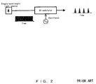
- Figs. 1 through 3 show the configurations of the prior art.
- a data light source that stably outputs data light with bit rate that accurately meets the requirements of the system generally modulates by data using an intensity modulator 10.
- data light can be always generated in synchronization with the bit rate of a system.
- its duty rate is approximately 2, and it must be improved.
- a mode-locking method as one of the technologies for generating an optical clock with high duty rate.
- duty rate is improved by exciting a standing wave in a resonator composed of a gain medium, a wavelength selector and a modulator.
- a mode-locked semiconductor laser and a mode-locked fiber laser as such a light source.
- For these light sources see, for example, Non-patent reference 2.
- the oscillation of data light by these mode locked lasers has an advantage of easily generating optical clocks with high duty rate, it has also a problem that its device configuration becomes complex and its size becomes large.
- the repetition frequency of an optical clock depends on the length of a resonator, and the length of the resonator fluctuates due to the change of an external environment and the fluctuations of temperature. Therefore, a large-scale stabilization device is indispensable for the stable generation of optical clocks.
- Non-patent reference 1 IEE Electron. Lett., vol. 31, page 671, 1995
- Non-patent reference 2 Journal of The Institute of Electronics, Information and Communication Engineers, C-1, J80-C-1, page 70, February 1997.
- the mode-locked clock light source can generate optical pulses with high OSNR and pulse width of pico-seconds or subpico-seconds.
- the conventional method for applying an optical gate to CW light using an intensity modulator and generating data light can be easily realized by a configuration simpler than a mode locked laser pulse light source, it has a problem that it is difficult to generate optical pulses with high duty rate and the like.
- the optical device of the present invention comprises a CW light generation unit generating CW light, a phase modulation unit modulating the CW light by phase and an optical pulse generation unit generating optical pulses by compensating for frequency chirp generated in the phase-modulated CW light by the phase modulation.
- optical pulses are not directly generated by modulating by intensity, optical pulses whose pulse width is narrower than the operational limit of an electrical circuit can be generated. Since the present invention requires no cavity configuration when optical pulses are generated, stable optical pulses with narrow pulse width that are strong against the manufacturing limit of the cavity and an environmental change, such as a temperature change and the like can be generated.
- the generation of data light with high duty rate and pulse width of pico-seconds or subpico-seconds without being restricted by the frequency of a modulation signal, whose control is easy, which accurately and stably operates in an arbitrary repetition frequency can be realized.
- the downsizing and cost reduction of a data light source device can be realized, and its reliability can be improved.
- Fig. 4 shows the configuration of the first preferred embodiment of the present invention.
- Fig. 4 shows the configuration of a short-pulse data light source adopting a modulation method according to the first preferred embodiment of the present invention.
- An LN (LiNbO 3 ) optical phase modulator 21 applies frequency chirp to light outputted from a single -wavelength laser light source 20 by an electrical data signal. Then, if a dispersion medium 22 compensates for the frequency chirp, specifically adjusts the phase relationship of the light in such a way that its phase does not change on a time axis, a solitary wave (data light) can be obtained.
- semiconductor DFB laser or DBR laser is used for the single-wavelength laser light source 20.
- the optical phase modulator induces frequency chirp to CW light.
- a 10-40Gb/s electrical signal is used for the optical phase modulator.
- a single-mode optical fiber (SMF) or a dispersion-compensating fiber (DCF) is used for the compensator of frequency chirp.
- a liquid crystal space optical phase modulator can also be used.
- the liquid crystal space optical phase modulator can arbitrarily operate the phase of an optical spectrum in a frequency domain, and can independently control the phases of all optical frequency spectral components generated by a frequency chirp generation device.
- an AWG type optical phase modulator is used for another component for compensating for frequency chirp.
- the operation of this modulator is the same as that of the liquid crystal space optical phase modulator.
- a waveguide is formed on a silicon substrate, and light to which frequency chirp has been applied on the principles of a phased array antenna is Fourier -transferred into a frequency domain. Then, the phase of an optical frequency is operated on a Fourier plane. Then, by inverse-Fourier-transferring the light into a time domain, all the phases of frequency spectral components can be independently controlled.
- optical clocks can be generated.
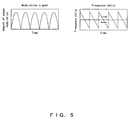
- a method for modulating light by the above-described phase modulator using a parabola-shaped signal is also effective.
- This signal can be realized by an electrical circuit within the speed range up to approximately 10GHz.
- Fig. 5 shows the phase modulation and frequency chirp.
- the positional order between a mechanism for applying frequency chirp and a mechanism for compensating for the chirp can also be the reversal of that shown in Fig. 4.
- Fig. 6 shows the configuration of the second preferred embodiment of the present invention.
- the single-wavelength laser light source 25 and frequency chirp generation device 26 are the same as those of the first preferred embodiment, respectively.
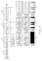
- An electrical data signal or sine wave signal with the same frequency as that of the electrical data signal applied to the optical phase modulator in order to generate frequency chirp is applied to an optical intensity modulator 27.
- Waveforms shown in Fig. 6 sequentially indicate the phase, frequency chirp characteristic and optical waveform of phase modulation light from top, and indicate the timing of an RF data signal to be applied to the optical intensity modulator and optical phase modulator.
- the optical intensity modulator is driven in the timing when the respective phases of the phase modulator and intensity modulator are the same (or reverse, that is, are shifted only by ⁇ ).
- the bottom graph is an example of the modulation in the timing when the respective phases of the phase modulator and intensity modulator are the same.
- the optical intensity modulator applies a time gate only to the shaded part, and only linear frequency chirp is extracted.
- an LN modulator with a Mach-Zehnder configuration or an InP modulator is used, but the modulator is not limited to these modulators.
- the chirp of an optical pulse whose frequency chirp is compensated for by a linear dispersion medium. By making the phases of all the frequency spectral components the same, the optical pulse becomes a TL pulse.
- an optical fiber single-mode fiber, dispersion-compensating fiber
- a photonic crystal fiber a chirp type fiber Bragg grading
- a liquid crystal space optical phase modulator a liquid crystal space optical phase modulator
- an AWG type optical phase modulator or the like is used, but the medium is not limited to these.
- the positional order between the optical phase modulator, optical intensity modulator and dispersion medium is not limited to that shown in Fig. 6, and an arbitrary order can be applied. If a hybrid modulator obtained by integrating the optical phase modulator and optical intensity modulator is adopted, the insertion loss of a modulator can be reduced, and optical pulses each with a better optical SNR characteristic can be generated.
- Fig. 7 shows the configuration of the third preferred embodiment of the present invention.
- the waveform of data light to be calculated varies depending the application of a generated optical pulse. For example, in a communication system using an optical soliton, a Sech type waveform is needed.
- Light with an arbitrary pulse shape can be obtained by a function to control the intensity of a frequency spectrum.
- a method for realizing a data light source with this function is described below. Its configuration is shown in Fig. 7, and is the same as that of the second preferred embodiment except for an optical intensity filter 29.
- the optical intensity filter 29 can be realized by using a filter having a transmission characteristic for realizing a desired optical intensity spectral characteristic.
- a dielectric multi-layered film type optical bandpass filter for example, a dielectric multi-layered film type optical bandpass filter, an AWG type optical bandpass filter, a fiber Bragg grating optical bandpass filter, a Fabry-Perot type optical bandpass filter, a photonic crystal type filter or a liquid crystal space optical intensity modulator is used, but the filter is not limited to these filters.
- the positional order between the frequency chirp generation device, optical intensity modulator, frequency chirp compensator (dispersive medium) and optical intensity filter any order can be applied as long as the optical intensity filter is located after the frequency chirp generation device and optical intensity modulator.
- the data light source can be realized by the above-described method even in any order other than that shown in Fig. 7. If electrical data signals are all "1" or sine wave signals, optical clocks can be generated.
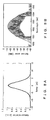
- Figs. 8A and 8B show the optical clock and its optical spectrum actually realized by this preferred embodiment.
- Figs. 8A and 8B show the shape of a realized optical pulse and its optical spectrum, respectively.
- the optical phase modulator generates frequency chirp by applying phase modulation with a modulation factor of 6.1 ⁇ to CW light with a wavelength of 1,552.2 nm, and the optical intensity modulator transforms the CW light into a pulse by extracting only linear frequency chirp with the same phase as the phase modulator.
- the dielectric multi-layered film type optical bandpass filter adjusts the intensity characteristic of its optical spectrum so as to take a Gaussian shape.
- the phases of optical frequency spectral components are adjusted by a single-mode optical fiber with dispersion of 9.
- a TL pulse with a pulse width of 3.8ps is realized at a 10 GHz repetition frequency. It is the amount of the frequency chirp generated the optical phase modulator that prevents the generation of a further shorter realized optical pulse, which restricts the bandwidth of the envelope of the optical frequency components.
- a pulse with further shorter pulse width can be generated by generating optical frequency spectral components with a broad bandwidth by the following methods.
- Fig. 9 shows the configuration of the fourth preferred embodiment of the present invention.
- This method differs from the above-described one only in that the same number of single-wavelength laser light sources 25-1 through 25-n as the desired number (n) of multi-wavelength light sources are prepared and an optical multiplexer 30 multiplexes a plurality of segments of light outputted from these light sources.
- an AWG type optical multiplexer, an optical interleaver, an optical fiber multiplexer or the like is used, but the optical multiplexer is not limited to these.
- a filter with a plurality of transmission center frequencies such as a Fabry-Perot type optical bandpass filter or the like is used, and one with one input port and one output port is effective when multi-wavelength pulse light is generated in one fiber.
- a Fabry-Perot type optical bandpass filter or the like is used, and one with one input port and one output port is effective when multi-wavelength pulse light is generated in one fiber.
- the optical modulator modulates multi-wavelength optical clocks generated in this preferred embodiment by data for each wavelength
- an AWG type optical transmission filter is convenient for demultiplexing wavelengths.
- polarization maintaining type components maintaining the polarization of light By using polarization maintaining type components maintaining the polarization of light in the above-described preferred embodiments, stable pulse light source whose optical pulse characteristic is not degraded by polarization fluctuations that are generated by an external environmental change, a temperature change or the like, can be realized.
- optical clock applications realized by the above-described modulation methods are described below.
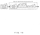
- Fig. 10 shows the configuration of the fifth preferred embodiment of the present invention.
- this preferred embodiment generates 10GHz or 40GHz optical pulses and an optical time-division multiplexing device 36 multiplexes these pulses in a time domain.
- an optical branching filter 37 branches an inputted optical pulse for two routes, a delayer 38 applies a delay to one route and then, a photo-coupler 39 couples respective optical pulses that have been transmitted through the two routes, again.
- the delayer 38 an optical fiber or a space type optical delay circuit is used, but the delayer is not limited to these.
- a method for doubling a repetition frequency is described.
- Fig. 11 shows the configuration of the sixth preferred embodiment of the present invention.
- an optical branching coupler 40 branches an ultra-high-optical signal (bit rate B (B ⁇ 100Gb/s) into two signals.
- a clock extraction circuit 43 extracts an electrical clock (B/n) with speed that can be electrically processed from one branched signal light, and the pulse light source device 35 of the present invention is driven by the electrical clock.
- the optical time-division multiplexing device 36 generates an optical clock with a high frequency by the method shown in the fifth preferred embodiment.
- the other signal branched by the optical branching coupler 40 is amplified by an optical amplifier 41 and is inputted to an optical switch 42.
- the other ultra-high-speed signal light branched by the optical branching coupler 40 switches this optical clock in the optical switch 42. Since the actually received optical signal is replaced with the generated optical clock thus, the 3R regeneration of an ultra-high-speed signal light can be realized.
- an optical fiber branching filter or the like can be used for the optical branching coupler 40.
- a time-division multiplexing circuit using an EA modulator converts the light signal into a low-speed (B/n) signal light
- the clock extraction circuit 43 extracts a clock in an electronic circuit.
- the optical switch 42 for switching an ultra-high-speed optical clock an optical Kerr switch, a non-linear optical loop mirror switch, an optical four-wave mixing switch or the like is used, but the optical switch is not limited to these.
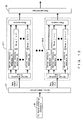
- Fig. 12 shows the configuration of the seventh preferred embodiment of the present invention.
- An optical branching filter 45 branches an optical pulse generated by the pulse light source 35 of the present invention into a plurality of optical pulses.
- an optical pulse is branched into n pulses.
- Each of optical intensity modulator 46-1 through 46-n puts a data signal on one branched optical pulse.
- Each of delayers 47-1 through 47-(n-1) applies an appropriate delay to each optical pulse signal modulated by data so that the optical pulse signals may not timewise overlap when a photo-coupler couples them, and then the photo-coupler 48 couples all the optical signal pulses.
- a delay time ( ⁇ ) of 6.25ps is obtained.
- an optical fiber branching filter and an optical fiber coupler respectively, can be used.
- the data modulation can be realized by an LN modulator or an InP modulator.
- an optical fiber or space type optical delay circuit is used.
- Fig. 13 shows the configuration of the eighth preferred embodiment of the present invention.
- an optical demultiplexer demultiplexes an optical pulse outputted from the multi-wavelength pulse light source 50 described in the fourth preferred embodiment for each wavelength.
- Each of blocks 52-1 through 52-m time-division multiplexes each optical pulse demultiplexed for each wavelength by the method described in the seventh preferred embodiment, and then an optical multiplexer 53 multiplexes them by wavelength again.
- an AWG light filter or an interleaver is used for the optical demultiplexer 51/multiplexer 53.
- Fig. 14 shows the configuration of the ninth preferred embodiment of the present invention.
- the pulse light source 35 of the present invention uses the pulse light source 35 of the present invention as a multi-wavelength light source.
- a wavelength demultiplexer 61 extracts each modulation spectral component from the optical pulse whose spectrum has been expanded.
- the details of the spectrum expansion device 60 are disclosed in the already applied patent laid-open publication (No. 2002-77052) . If the absolute wavelength of the CW light source is set to the wavelength specified for WDM signals in ITU-T and the modulation frequency is set to the frequency specified for WDM signals in ITU-T, a plurality of CW light sources for WDM signals can be realized by this preferred embodiment. This has an advantage that the absolute wavelength of each wavelength can be collectively controlled by only the absolute wavelength and modulation frequency of a CW light source in the pulse light source.
- Fig. 15 shows the configuration of the tenth preferred embodiment of the present invention.
- the spectrum expansion device 60 does not function if pulse waves timewise overlap. Therefore, the pulse delayer 65 applies a time difference to each optical pulse so that pulses with different wavelengths may not overlap.
- the time-division multiplex device described in the fifth preferred embodiment can realize this. In this case, the spectrum expansion device 60 expands the spectrum of an optical pulse with a different wavelength outputted from the pulse delayer 65, and a wavelength demultiplexer 61 extracts each modulation spectral component to transform the optical pulse into CW light.
- high-order modulation components are generated by applying frequency chirp whose phase changes on a time axis to CW light outputted from a laser light source. Then, the generated high-order modulation components are transformed into pulses by making the respective phases of the generated high-order modulation components the same.
- An optical intensity filter that adjusts the envelope of the optical spectra is used to generate an optical pulse with a desired waveform.
- the preferred embodiment also has the features of a data light source obtained by combining a CW light source and an intensity modulator, and accordingly it can generate data light with high duty rate.
- the present invention CW light source + intensity modulator Clock light source + intensity modulator Configuration o ⁇ Simple o ⁇ Simple ⁇ Complex Duty rate o ⁇ > 100 @10Gb/s ⁇ 2 ⁇ 20 @10Gb/s o ⁇ > 100 @10Gb/s Synchronization with external signal o ⁇ Can be synchronized by oscillator o ⁇ Can be synchronized by oscillator ⁇ Fluctuations of resonator length resonator length Jitter o ⁇ Jitter of electrical data signal o ⁇ Jitter of electrical data signal ⁇ Fluctuations of resonator length on clock light source Size o ⁇ 19-inch rack, one step o ⁇ 19-inch rack, one step ⁇ 19-inch rack, five
Landscapes
- Physics & Mathematics (AREA)
- Electromagnetism (AREA)
- Engineering & Computer Science (AREA)
- Computer Networks & Wireless Communication (AREA)
- Signal Processing (AREA)
- Optical Modulation, Optical Deflection, Nonlinear Optics, Optical Demodulation, Optical Logic Elements (AREA)
- Optical Communication System (AREA)
Abstract
Description
| The present invention | CW light source + intensity modulator | Clock light source + intensity modulator | |
| Configuration | o ○ Simple | o ○ Simple | × Complex |
| Duty rate | o ○ > 100 @10Gb/s | × 2~20 @10Gb/s | o ○ > 100 @10Gb/s |
| Synchronization with external signal | o ○ Can be synchronized by oscillator | o ○ Can be synchronized by oscillator | Δ Fluctuations of resonator length resonator length |
| Jitter | o ○ Jitter of electrical data signal | o ○ Jitter of electrical data signal | Δ Fluctuations of resonator length on clock light source |
| Size | o ○ 19-inch rack, one step | o ○ 19-inch rack, one step | Δ 19-inch rack, five steps |
Claims (21)
- An optical device, comprising:continuous wave (CW) light generation means for generating continuous wave light;phase modulation means for modulating the CW light by phase; andoptical pulse generation means for generating optical pulses by compensating for frequency chirp generated in the phase-modulated CW light by phase modulation.
- The optical device according to claim 1, further comprising:intensity modulation means for modulating the phase-modulated CW light by intensity and extracting only linear frequency chirp.
- The optical device according to claim 1, further comprising:optical spectrum adjustment means for adjusting an intensity shape of an optical spectrum of the optical pulse generated by said optical pulse generation means and obtaining an optical pulse with a desired waveform.
- The optical device according to claim 1, further comprising:delay means for branching the generated optical pulse and applying a time delay to each branched optical pulse; andmultiplexing means for generating an optical pulse with a higher repetition frequency by multiplexing the delayed optical pulses.
- The optical device according to claim 1, further comprising:optical spectrum expansion means for expanding an optical spectrum of the generated optical pulse; andseparation means for separating each modulation spectral component constituting the expanded optical spectrum and obtaining CW light.
- An optical 3R regenerator , comprising:clock extraction means for extracting a clock from an optical signal that propagates through a transmission line;said optical device according to claim 4 that operates according to the clock; andswitch means for switching optical pulses outputted from said optical device, using the optical signal.
- The optical device according to claim 1, which comprises said CW light generation means for each different wavelength, and both said phase modulation means and optical pulse generation means transform wavelength-multiplexed light obtained by multiplexing a plurality of segments of the CW light into an optical pulse.
- The optical device according to claim 7, further comprising:intensity modulation means for modulating the phase-modulated CW light by intensity and extracting only linear frequency chirp.
- The optical device according to claim 7, further comprising:optical spectrum adjustment means for adjusting an intensity shape of an optical spectrum of the optical pulse generated by said optical pulse generation means and obtaining an optical pulse with a desired waveform.
- The optical device according to claim 7, further comprising:wavelength demultiplexing means for demultiplexing the optical pulse composed of a plurality of optical pulses each with a different wavelength per each wavelength;delay means for branching each optical pulse demultiplexed for each wavelength and applying a time delay to each branched optical pulse;couplingmeans for generating an optical pulse with a higher repetition frequency by coupling differently delayed optical pulses; andwavelength multiplexing means for multiplexing a plurality of optical pulses each with a high repetition frequency.
- The optical device according to claim 7, further comprising:wavelength demultiplexing means for demultiplexing the optical pulse composed of a plurality of optical pulses each with a different wavelength for each wavelength;wavelength delay means for applying a delay time different for each wavelength to each demultiplexed optical pulse for each wavelength; andoptical spectrum expansion means for expanding an optical spectrum of each delayed optical pulse; andseparation means for separating the expanded optical spectrum into each modulation spectral components and obtaining CW light.
- The optical device according to claim 1, wherein
the phase modulation generates data light using a data signal. - The optical device according to claim 1, wherein
the phase modulation generates clock light using a clock signal. - The optical device according to claim 1, wherein
said CW light generation means is either DFB laser or DBR laser. - The optical device according to claim 1, wherein
said phase modulation means is either a lithium niobate modulator or an indium phosphorus modulator. - The optical device according to claim 1, wherein
said optical pulse generation means is one of an optical fiber, a photonic crystal fiber, a liquid crystal space phase modulator and an arrayed waveguide type phase modulator. - The optical device according to claim 2 or 8, wherein
said intensity modulation means is either Mach-Zehnder modulator using lithium niobate or indium phosphorus as a material, or a liquid crystal space optical intensity modulator. - The light source according to claim 3, wherein
said optical spectrum adjustment means is one of a dielectric multi-layered film type optical bandpass filter, an arrayed waveguide type optical bandpass filter, a fiber Bragg grating optical bandpass filter, a Fabry-Perot type optical bandpass filter, a photonic crystal type filter and a liquid crystal space optical intensity modulator. - The light source according to claim 9, wherein
said optical spectrum adjustment means is one of a dielectric multi-layered film type optical bandpass filter, an arrayedwaveguide type optical bandpass filter, a fiber Bragg grating optical bandpass filter, a Fabry-Perot type optical bandpass filter, a photonic crystal type filter and a liquid crystal space optical intensity modulator. - The light source according to claim 16, wherein
said optical pulse generation means is composed of polarization maintaining components. - The light source according to claim 18 or 19, wherein
said optical pulse generation means is composed of polarization maintaining components.
Applications Claiming Priority (2)
| Application Number | Priority Date | Filing Date | Title |
|---|---|---|---|
| JP2004050794A JP4444689B2 (en) | 2004-02-26 | 2004-02-26 | Optical device for optical communication |
| JP2004050794 | 2004-02-26 |
Publications (2)
| Publication Number | Publication Date |
|---|---|
| EP1569367A2 true EP1569367A2 (en) | 2005-08-31 |
| EP1569367A3 EP1569367A3 (en) | 2007-08-22 |
Family
ID=34747489
Family Applications (1)
| Application Number | Title | Priority Date | Filing Date |
|---|---|---|---|
| EP04014150A Ceased EP1569367A3 (en) | 2004-02-26 | 2004-06-16 | Optical device for optical communication |
Country Status (3)
| Country | Link |
|---|---|
| US (1) | US7433564B2 (en) |
| EP (1) | EP1569367A3 (en) |
| JP (1) | JP4444689B2 (en) |
Cited By (7)
| Publication number | Priority date | Publication date | Assignee | Title |
|---|---|---|---|---|
| WO2005084268A2 (en) | 2004-02-27 | 2005-09-15 | Azna Llc | Fm source and spectral reshaping element |
| EP2224625A1 (en) * | 2009-02-27 | 2010-09-01 | Fujitsu Limited | Optical signal processing device and method of processing optical signal |
| WO2011153813A1 (en) * | 2010-06-11 | 2011-12-15 | Zhou Yunwei | Multiplex communication method based on fm/chirp modulation and application systems thereof |
| CN104678595A (en) * | 2015-02-09 | 2015-06-03 | 中国电子科技集团公司第二十三研究所 | Laser phase modulation method capable of effectively suppressing amplitude frequency effect |
| CN111623902A (en) * | 2020-06-05 | 2020-09-04 | 上海交通大学 | Distributed optical fiber Raman temperature sensor based on intensity modulation chirp pulse compression |
| WO2021255342A1 (en) * | 2020-06-16 | 2021-12-23 | Teknologian Tutkimuskeskus Vtt Oy | Optical arbitrary pulse pattern generator |
| US12283995B2 (en) | 2020-06-16 | 2025-04-22 | Teknologian Tutkimuskeskus Vtt Oy | Cryogenic waveform source |
Families Citing this family (10)
| Publication number | Priority date | Publication date | Assignee | Title |
|---|---|---|---|---|
| US7076120B2 (en) * | 2002-07-08 | 2006-07-11 | Lucent Technologies Inc. | Optical pulse generator for return-to-zero signaling |
| GB2446528B (en) | 2005-09-27 | 2010-11-24 | Fujitsu Ltd | Optical signal multiplexing device and optical signal multiplexing method |
| WO2007148377A1 (en) | 2006-06-19 | 2007-12-27 | Fujitsu Limited | Optical signal processor |
| JP4823800B2 (en) * | 2006-08-01 | 2011-11-24 | 日本電信電話株式会社 | Method and apparatus for stabilizing optical output of optical switch |
| JP5291952B2 (en) * | 2008-03-03 | 2013-09-18 | 日立アロカメディカル株式会社 | Ultrasonic diagnostic equipment |
| JP5824912B2 (en) * | 2011-06-29 | 2015-12-02 | 富士通株式会社 | Optical transmission apparatus and optical interleave control method |
| US9366937B2 (en) * | 2012-01-13 | 2016-06-14 | Sumitomo Osaka Cement Co., Ltd. | Optical pulse-generator |
| US10419147B2 (en) * | 2014-09-03 | 2019-09-17 | Alcatel Lucent | Optical line loading using variable bandwidth noise |
| US10707837B2 (en) * | 2017-07-06 | 2020-07-07 | Analog Photonics LLC | Laser frequency chirping structures, methods, and applications |
| EP4096509B1 (en) * | 2020-01-31 | 2026-03-25 | The General Hospital Corporation | Frequency-comb generation based on electro-optic phase-code mode-locking for circular-ranging oct |
Citations (3)
| Publication number | Priority date | Publication date | Assignee | Title |
|---|---|---|---|---|
| EP0622916A1 (en) * | 1993-04-30 | 1994-11-02 | AT&T Corp. | Optical soliton generator |
| US20020015212A1 (en) | 2000-07-07 | 2002-02-07 | Masamichi Fujiwara | Multi-wavelength generating method and apparatus based on flattening of optical spectrum |
| US20040005110A1 (en) | 2002-07-08 | 2004-01-08 | Juerg Leuthold | Optical pulse generator for return-to-zero signaling |
Family Cites Families (15)
| Publication number | Priority date | Publication date | Assignee | Title |
|---|---|---|---|---|
| US5299210A (en) * | 1992-04-28 | 1994-03-29 | Rutgers University | Four-level multiply doped rare earth laser system |
| FR2743428B1 (en) * | 1996-01-08 | 1998-01-30 | Dupont Laurent | ELECTRO-OPTICAL PHASE MODULATOR FOR SINGLE-MODE FIBER OPTICS |
| AU1525799A (en) * | 1997-11-18 | 1999-06-07 | California Institute Of Technology | Sampling of electronic signals using optical pulses |
| US6335819B1 (en) * | 1999-02-19 | 2002-01-01 | University Of Maryland | All-optical regeneration at high bit rates using an electroabsorption modulator |
| US6366356B1 (en) * | 1999-04-01 | 2002-04-02 | Trw Inc. | High average power fiber laser system with high-speed, parallel wavefront sensor |
| AU2001247338A1 (en) * | 2000-03-09 | 2001-09-17 | Optium, Inc. | Apparatuses and methods for generating optical signals |
| US6876818B1 (en) * | 2000-08-18 | 2005-04-05 | Futurewei Technologies, Inc. | Method and system for transmitting signals with spectrally enriched optical pulses |
| JP2002077051A (en) * | 2000-08-31 | 2002-03-15 | Fujitsu Ltd | Optical signal processing device |
| JP3948598B2 (en) | 2000-09-01 | 2007-07-25 | 富士通株式会社 | Method, apparatus and system for processing optical signals |
| US6766070B2 (en) * | 2001-04-27 | 2004-07-20 | The United States Of America As Represented By The Secretary Of The Navy | High power fiber optic modulator system and method |
| US6804428B1 (en) * | 2001-11-14 | 2004-10-12 | Capella Photonics, Inc. | Optical spectral power monitors employing polarization deversity scheme |
| US20040208543A1 (en) * | 2002-03-13 | 2004-10-21 | Gigatera Ag | Multiplexer and pulse generating laser device |
| USH2190H1 (en) * | 2002-06-11 | 2007-06-05 | The United States Of America As Represented By The Secretary Of The Air Force | Sampled analog transmission |
| US7023890B2 (en) * | 2002-06-17 | 2006-04-04 | Alfonso Benjamin Amparan | Digital optical sourcing and methods of operating a digital optical source |
| US7171082B2 (en) * | 2003-07-18 | 2007-01-30 | Hrl Laboratories, Llc | Method and apparatus for optical top-hat pulse generation |
-
2004
- 2004-02-26 JP JP2004050794A patent/JP4444689B2/en not_active Expired - Fee Related
- 2004-05-25 US US10/852,203 patent/US7433564B2/en not_active Expired - Lifetime
- 2004-06-16 EP EP04014150A patent/EP1569367A3/en not_active Ceased
Patent Citations (3)
| Publication number | Priority date | Publication date | Assignee | Title |
|---|---|---|---|---|
| EP0622916A1 (en) * | 1993-04-30 | 1994-11-02 | AT&T Corp. | Optical soliton generator |
| US20020015212A1 (en) | 2000-07-07 | 2002-02-07 | Masamichi Fujiwara | Multi-wavelength generating method and apparatus based on flattening of optical spectrum |
| US20040005110A1 (en) | 2002-07-08 | 2004-01-08 | Juerg Leuthold | Optical pulse generator for return-to-zero signaling |
Cited By (10)
| Publication number | Priority date | Publication date | Assignee | Title |
|---|---|---|---|---|
| WO2005084268A2 (en) | 2004-02-27 | 2005-09-15 | Azna Llc | Fm source and spectral reshaping element |
| EP1738504A4 (en) * | 2004-02-27 | 2017-04-19 | Finisar Corporation | Optical system comprising an fm source and a spectral reshaping element |
| EP2224625A1 (en) * | 2009-02-27 | 2010-09-01 | Fujitsu Limited | Optical signal processing device and method of processing optical signal |
| WO2011153813A1 (en) * | 2010-06-11 | 2011-12-15 | Zhou Yunwei | Multiplex communication method based on fm/chirp modulation and application systems thereof |
| CN104678595A (en) * | 2015-02-09 | 2015-06-03 | 中国电子科技集团公司第二十三研究所 | Laser phase modulation method capable of effectively suppressing amplitude frequency effect |
| CN111623902A (en) * | 2020-06-05 | 2020-09-04 | 上海交通大学 | Distributed optical fiber Raman temperature sensor based on intensity modulation chirp pulse compression |
| WO2021255342A1 (en) * | 2020-06-16 | 2021-12-23 | Teknologian Tutkimuskeskus Vtt Oy | Optical arbitrary pulse pattern generator |
| US20230221613A1 (en) * | 2020-06-16 | 2023-07-13 | Teknologian Tutkimuskeskus Vtt Oy | Optical arbitrary pulse pattern generator |
| US12283995B2 (en) | 2020-06-16 | 2025-04-22 | Teknologian Tutkimuskeskus Vtt Oy | Cryogenic waveform source |
| US12449707B2 (en) * | 2020-06-16 | 2025-10-21 | Teknologian Tutkimuskeskus Vtt Oy | Optical arbitrary pulse pattern generator |
Also Published As
| Publication number | Publication date |
|---|---|
| US20050190432A1 (en) | 2005-09-01 |
| US7433564B2 (en) | 2008-10-07 |
| JP4444689B2 (en) | 2010-03-31 |
| JP2005241902A (en) | 2005-09-08 |
| EP1569367A3 (en) | 2007-08-22 |
Similar Documents
| Publication | Publication Date | Title |
|---|---|---|
| US7433564B2 (en) | Optical device for optical communication | |
| CA2389974C (en) | Multi-wavelength optical modulation circuit and wavelength-division multiplexed optical signal transmitter | |
| Ellis et al. | Ultra-high-speed OTDM networks using semiconductor amplifier-based processing nodes | |
| US6204944B1 (en) | All-optical time-division demultiplexing circuit and all-optical TDM-WDM conversion circuit | |
| EP1303932B1 (en) | Optical pulse train generator | |
| US8190032B2 (en) | Optical signal processing apparatus | |
| KR19980071330A (en) | Multi-wavelength light source and optical signal generation method | |
| EP0787390A1 (en) | All-optical processing in communications systems | |
| US20010053008A1 (en) | Optical pulse generating apparatus and optical signal apparatus using the same | |
| Olsson et al. | WDM to OTDM multiplexing using an ultrafast all-optical wavelength converter | |
| Connelly | Semiconductor optical amplifiers and their applications | |
| US7623792B2 (en) | Clock extracting method and apparatus thereof | |
| JP4495415B2 (en) | OTDM transmission method and apparatus | |
| JP3447664B2 (en) | Optical transmitter and optical transmitter control method | |
| JP4252470B2 (en) | OTDM / WDM transmission method and apparatus | |
| KR19990082561A (en) | Optical pulse source and its generation method | |
| Mima et al. | A novel wavelength converter based on optical single-sideband modulator and arrayed waveguide grating | |
| Suzuki et al. | Recent progress in optical soliton communication | |
| EP1571765B1 (en) | Optical synchronizer | |
| EP1575194A2 (en) | Pulse generating apparatus and method | |
| Saruwatari | All-optical time-division multiplexing technology | |
| JPH0818539A (en) | Optical time division multiplexing signal separation method | |
| Bogoni et al. | Demonstration of feasibility of a complete 160 Gbit/s OTDM system including all-optical 3R | |
| JP2007124026A (en) | Method and apparatus for extracting optical clock signal | |
| MORIOKA | Ultrafast optical technologies for large-capacity OTDM/WDM transmission |
Legal Events
| Date | Code | Title | Description |
|---|---|---|---|
| PUAI | Public reference made under article 153(3) epc to a published international application that has entered the european phase |
Free format text: ORIGINAL CODE: 0009012 |
|
| AK | Designated contracting states |
Kind code of ref document: A2 Designated state(s): AT BE BG CH CY CZ DE DK EE ES FI FR GB GR HU IE IT LI LU MC NL PL PT RO SE SI SK TR |
|
| AX | Request for extension of the european patent |
Extension state: AL HR LT LV MK |
|
| PUAL | Search report despatched |
Free format text: ORIGINAL CODE: 0009013 |
|
| AK | Designated contracting states |
Kind code of ref document: A3 Designated state(s): AT BE BG CH CY CZ DE DK EE ES FI FR GB GR HU IE IT LI LU MC NL PL PT RO SE SI SK TR |
|
| AX | Request for extension of the european patent |
Extension state: AL HR LT LV MK |
|
| RIC1 | Information provided on ipc code assigned before grant |
Ipc: H04B 10/18 20060101AFI20070719BHEP |
|
| 17P | Request for examination filed |
Effective date: 20070817 |
|
| 17Q | First examination report despatched |
Effective date: 20071127 |
|
| AKX | Designation fees paid |
Designated state(s): DE FR GB |
|
| APBK | Appeal reference recorded |
Free format text: ORIGINAL CODE: EPIDOSNREFNE |
|
| APBN | Date of receipt of notice of appeal recorded |
Free format text: ORIGINAL CODE: EPIDOSNNOA2E |
|
| APBR | Date of receipt of statement of grounds of appeal recorded |
Free format text: ORIGINAL CODE: EPIDOSNNOA3E |
|
| APAF | Appeal reference modified |
Free format text: ORIGINAL CODE: EPIDOSCREFNE |
|
| APBT | Appeal procedure closed |
Free format text: ORIGINAL CODE: EPIDOSNNOA9E |
|
| STAA | Information on the status of an ep patent application or granted ep patent |
Free format text: STATUS: THE APPLICATION HAS BEEN REFUSED |
|
| 18R | Application refused |
Effective date: 20160708 |