EP1569287A2 - Organic light emitting device materials and organic light emitting devices - Google Patents
Organic light emitting device materials and organic light emitting devices Download PDFInfo
- Publication number
- EP1569287A2 EP1569287A2 EP05004110A EP05004110A EP1569287A2 EP 1569287 A2 EP1569287 A2 EP 1569287A2 EP 05004110 A EP05004110 A EP 05004110A EP 05004110 A EP05004110 A EP 05004110A EP 1569287 A2 EP1569287 A2 EP 1569287A2
- Authority
- EP
- European Patent Office
- Prior art keywords
- diyl
- formula
- independently represent
- compound represented
- light
- Prior art date
- Legal status (The legal status is an assumption and is not a legal conclusion. Google has not performed a legal analysis and makes no representation as to the accuracy of the status listed.)
- Withdrawn
Links
- 239000000463 material Substances 0.000 title description 32
- 150000001875 compounds Chemical class 0.000 claims abstract description 69
- 125000004432 carbon atom Chemical group C* 0.000 claims abstract description 24
- 125000001424 substituent group Chemical group 0.000 claims abstract description 18
- 125000005842 heteroatom Chemical group 0.000 claims abstract description 16
- 125000005647 linker group Chemical group 0.000 claims abstract description 10
- 125000003118 aryl group Chemical group 0.000 claims abstract description 9
- 125000000623 heterocyclic group Chemical group 0.000 claims abstract description 6
- 125000004122 cyclic group Chemical group 0.000 claims abstract description 5
- -1 thiophene-2,5-diyl Chemical group 0.000 claims description 64
- 125000000217 alkyl group Chemical group 0.000 claims description 25
- 239000007788 liquid Substances 0.000 claims description 16
- 238000006116 polymerization reaction Methods 0.000 claims description 8
- 125000003545 alkoxy group Chemical group 0.000 claims description 4
- 125000002947 alkylene group Chemical group 0.000 claims description 4
- 229910052757 nitrogen Inorganic materials 0.000 claims description 4
- 125000004433 nitrogen atom Chemical group N* 0.000 claims description 4
- 125000001140 1,4-phenylene group Chemical group [H]C1=C([H])C([*:2])=C([H])C([H])=C1[*:1] 0.000 claims description 3
- 230000001747 exhibiting effect Effects 0.000 claims description 3
- 239000010410 layer Substances 0.000 description 66
- 238000000034 method Methods 0.000 description 34
- 239000010408 film Substances 0.000 description 29
- 239000000758 substrate Substances 0.000 description 19
- 230000010287 polarization Effects 0.000 description 18
- 238000002347 injection Methods 0.000 description 16
- 239000007924 injection Substances 0.000 description 16
- 239000011521 glass Substances 0.000 description 14
- 239000002904 solvent Substances 0.000 description 14
- 238000006243 chemical reaction Methods 0.000 description 11
- 239000004973 liquid crystal related substance Substances 0.000 description 11
- 230000000379 polymerizing effect Effects 0.000 description 11
- 239000000203 mixture Substances 0.000 description 10
- 238000000576 coating method Methods 0.000 description 9
- 229910052751 metal Inorganic materials 0.000 description 9
- 239000002184 metal Substances 0.000 description 9
- 239000003795 chemical substances by application Substances 0.000 description 8
- 229920000642 polymer Polymers 0.000 description 8
- 229920005989 resin Polymers 0.000 description 8
- 239000011347 resin Substances 0.000 description 8
- 239000003505 polymerization initiator Substances 0.000 description 7
- 229910052782 aluminium Inorganic materials 0.000 description 6
- XAGFODPZIPBFFR-UHFFFAOYSA-N aluminium Chemical compound [Al] XAGFODPZIPBFFR-UHFFFAOYSA-N 0.000 description 6
- 239000012044 organic layer Substances 0.000 description 6
- 229940125782 compound 2 Drugs 0.000 description 5
- 238000004132 cross linking Methods 0.000 description 5
- 238000007789 sealing Methods 0.000 description 5
- 239000000243 solution Substances 0.000 description 5
- 238000007740 vapor deposition Methods 0.000 description 5
- HEDRZPFGACZZDS-UHFFFAOYSA-N Chloroform Chemical compound ClC(Cl)Cl HEDRZPFGACZZDS-UHFFFAOYSA-N 0.000 description 4
- 239000004642 Polyimide Substances 0.000 description 4
- 239000011324 bead Substances 0.000 description 4
- 239000011248 coating agent Substances 0.000 description 4
- 239000004615 ingredient Substances 0.000 description 4
- PQXKHYXIUOZZFA-UHFFFAOYSA-M lithium fluoride Chemical compound [Li+].[F-] PQXKHYXIUOZZFA-UHFFFAOYSA-M 0.000 description 4
- 229920001721 polyimide Polymers 0.000 description 4
- 125000006850 spacer group Chemical group 0.000 description 4
- 239000010409 thin film Substances 0.000 description 4
- ZWEHNKRNPOVVGH-UHFFFAOYSA-N 2-Butanone Chemical compound CCC(C)=O ZWEHNKRNPOVVGH-UHFFFAOYSA-N 0.000 description 3
- 0 C*([Al](C(C)(C)C1=C*C(C(C)(C)*)=S1)I)I Chemical compound C*([Al](C(C)(C)C1=C*C(C(C)(C)*)=S1)I)I 0.000 description 3
- YMWUJEATGCHHMB-UHFFFAOYSA-N Dichloromethane Chemical compound ClCCl YMWUJEATGCHHMB-UHFFFAOYSA-N 0.000 description 3
- XEKOWRVHYACXOJ-UHFFFAOYSA-N Ethyl acetate Chemical compound CCOC(C)=O XEKOWRVHYACXOJ-UHFFFAOYSA-N 0.000 description 3
- ZMXDDKWLCZADIW-UHFFFAOYSA-N N,N-Dimethylformamide Chemical compound CN(C)C=O ZMXDDKWLCZADIW-UHFFFAOYSA-N 0.000 description 3
- 229910052799 carbon Inorganic materials 0.000 description 3
- 238000003618 dip coating Methods 0.000 description 3
- 239000003822 epoxy resin Substances 0.000 description 3
- 150000002148 esters Chemical class 0.000 description 3
- 238000000605 extraction Methods 0.000 description 3
- RAXXELZNTBOGNW-UHFFFAOYSA-N imidazole Natural products C1=CNC=N1 RAXXELZNTBOGNW-UHFFFAOYSA-N 0.000 description 3
- 239000004417 polycarbonate Substances 0.000 description 3
- 229920000515 polycarbonate Polymers 0.000 description 3
- 229920000647 polyepoxide Polymers 0.000 description 3
- 239000002356 single layer Substances 0.000 description 3
- 238000004528 spin coating Methods 0.000 description 3
- 239000000126 substance Substances 0.000 description 3
- GKWLILHTTGWKLQ-UHFFFAOYSA-N 2,3-dihydrothieno[3,4-b][1,4]dioxine Chemical compound O1CCOC2=CSC=C21 GKWLILHTTGWKLQ-UHFFFAOYSA-N 0.000 description 2
- UJOBWOGCFQCDNV-UHFFFAOYSA-N 9H-carbazole Chemical compound C1=CC=C2C3=CC=CC=C3NC2=C1 UJOBWOGCFQCDNV-UHFFFAOYSA-N 0.000 description 2
- 229920002284 Cellulose triacetate Polymers 0.000 description 2
- RTZKZFJDLAIYFH-UHFFFAOYSA-N Diethyl ether Chemical compound CCOCC RTZKZFJDLAIYFH-UHFFFAOYSA-N 0.000 description 2
- UFWIBTONFRDIAS-UHFFFAOYSA-N Naphthalene Chemical compound C1=CC=CC2=CC=CC=C21 UFWIBTONFRDIAS-UHFFFAOYSA-N 0.000 description 2
- ZCQWOFVYLHDMMC-UHFFFAOYSA-N Oxazole Chemical compound C1=COC=N1 ZCQWOFVYLHDMMC-UHFFFAOYSA-N 0.000 description 2
- 229920001609 Poly(3,4-ethylenedioxythiophene) Polymers 0.000 description 2
- 239000004793 Polystyrene Substances 0.000 description 2
- 239000004372 Polyvinyl alcohol Substances 0.000 description 2
- 239000004990 Smectic liquid crystal Substances 0.000 description 2
- WYURNTSHIVDZCO-UHFFFAOYSA-N Tetrahydrofuran Chemical compound C1CCOC1 WYURNTSHIVDZCO-UHFFFAOYSA-N 0.000 description 2
- YTPLMLYBLZKORZ-UHFFFAOYSA-N Thiophene Chemical compound C=1C=CSC=1 YTPLMLYBLZKORZ-UHFFFAOYSA-N 0.000 description 2
- NNLVGZFZQQXQNW-ADJNRHBOSA-N [(2r,3r,4s,5r,6s)-4,5-diacetyloxy-3-[(2s,3r,4s,5r,6r)-3,4,5-triacetyloxy-6-(acetyloxymethyl)oxan-2-yl]oxy-6-[(2r,3r,4s,5r,6s)-4,5,6-triacetyloxy-2-(acetyloxymethyl)oxan-3-yl]oxyoxan-2-yl]methyl acetate Chemical compound O([C@@H]1O[C@@H]([C@H]([C@H](OC(C)=O)[C@H]1OC(C)=O)O[C@H]1[C@@H]([C@@H](OC(C)=O)[C@H](OC(C)=O)[C@@H](COC(C)=O)O1)OC(C)=O)COC(=O)C)[C@@H]1[C@@H](COC(C)=O)O[C@@H](OC(C)=O)[C@H](OC(C)=O)[C@H]1OC(C)=O NNLVGZFZQQXQNW-ADJNRHBOSA-N 0.000 description 2
- 229910052783 alkali metal Inorganic materials 0.000 description 2
- 150000001340 alkali metals Chemical class 0.000 description 2
- 229910052784 alkaline earth metal Inorganic materials 0.000 description 2
- 150000001342 alkaline earth metals Chemical class 0.000 description 2
- IOJUPLGTWVMSFF-UHFFFAOYSA-N benzothiazole Chemical compound C1=CC=C2SC=NC2=C1 IOJUPLGTWVMSFF-UHFFFAOYSA-N 0.000 description 2
- 150000001721 carbon Chemical group 0.000 description 2
- 238000005266 casting Methods 0.000 description 2
- 239000003431 cross linking reagent Substances 0.000 description 2
- JHIVVAPYMSGYDF-UHFFFAOYSA-N cyclohexanone Chemical compound O=C1CCCCC1 JHIVVAPYMSGYDF-UHFFFAOYSA-N 0.000 description 2
- 238000000151 deposition Methods 0.000 description 2
- 230000005684 electric field Effects 0.000 description 2
- 125000001495 ethyl group Chemical group [H]C([H])([H])C([H])([H])* 0.000 description 2
- YLQWCDOCJODRMT-UHFFFAOYSA-N fluoren-9-one Chemical compound C1=CC=C2C(=O)C3=CC=CC=C3C2=C1 YLQWCDOCJODRMT-UHFFFAOYSA-N 0.000 description 2
- 125000005843 halogen group Chemical group 0.000 description 2
- 238000010438 heat treatment Methods 0.000 description 2
- 125000000959 isobutyl group Chemical group [H]C([H])([H])C([H])(C([H])([H])[H])C([H])([H])* 0.000 description 2
- 125000001449 isopropyl group Chemical group [H]C([H])([H])C([H])(*)C([H])([H])[H] 0.000 description 2
- 150000002576 ketones Chemical class 0.000 description 2
- 238000004519 manufacturing process Methods 0.000 description 2
- 125000002496 methyl group Chemical group [H]C([H])([H])* 0.000 description 2
- 125000004108 n-butyl group Chemical group [H]C([H])([H])C([H])([H])C([H])([H])C([H])([H])* 0.000 description 2
- 125000004123 n-propyl group Chemical group [H]C([H])([H])C([H])([H])C([H])([H])* 0.000 description 2
- WCPAKWJPBJAGKN-UHFFFAOYSA-N oxadiazole Chemical compound C1=CON=N1 WCPAKWJPBJAGKN-UHFFFAOYSA-N 0.000 description 2
- IEQIEDJGQAUEQZ-UHFFFAOYSA-N phthalocyanine Chemical compound N1C(N=C2C3=CC=CC=C3C(N=C3C4=CC=CC=C4C(=N4)N3)=N2)=C(C=CC=C2)C2=C1N=C1C2=CC=CC=C2C4=N1 IEQIEDJGQAUEQZ-UHFFFAOYSA-N 0.000 description 2
- 229920003023 plastic Polymers 0.000 description 2
- 239000004033 plastic Substances 0.000 description 2
- BASFCYQUMIYNBI-UHFFFAOYSA-N platinum Chemical compound [Pt] BASFCYQUMIYNBI-UHFFFAOYSA-N 0.000 description 2
- 229920003227 poly(N-vinyl carbazole) Polymers 0.000 description 2
- 229920003229 poly(methyl methacrylate) Polymers 0.000 description 2
- 229920000172 poly(styrenesulfonic acid) Polymers 0.000 description 2
- 229920002492 poly(sulfone) Polymers 0.000 description 2
- 229920000058 polyacrylate Polymers 0.000 description 2
- 229920000728 polyester Polymers 0.000 description 2
- 239000004926 polymethyl methacrylate Substances 0.000 description 2
- 229920002223 polystyrene Polymers 0.000 description 2
- 229940005642 polystyrene sulfonic acid Drugs 0.000 description 2
- 229920000123 polythiophene Polymers 0.000 description 2
- 229920002451 polyvinyl alcohol Polymers 0.000 description 2
- 238000002360 preparation method Methods 0.000 description 2
- 125000002914 sec-butyl group Chemical group [H]C([H])([H])C([H])([H])C([H])(*)C([H])([H])[H] 0.000 description 2
- 125000000999 tert-butyl group Chemical group [H]C([H])([H])C(*)(C([H])([H])[H])C([H])([H])[H] 0.000 description 2
- 150000003852 triazoles Chemical class 0.000 description 2
- UWRZIZXBOLBCON-VOTSOKGWSA-N (e)-2-phenylethenamine Chemical compound N\C=C\C1=CC=CC=C1 UWRZIZXBOLBCON-VOTSOKGWSA-N 0.000 description 1
- JYEUMXHLPRZUAT-UHFFFAOYSA-N 1,2,3-triazine Chemical compound C1=CN=NN=C1 JYEUMXHLPRZUAT-UHFFFAOYSA-N 0.000 description 1
- GEYOCULIXLDCMW-UHFFFAOYSA-N 1,2-phenylenediamine Chemical compound NC1=CC=CC=C1N GEYOCULIXLDCMW-UHFFFAOYSA-N 0.000 description 1
- BCMCBBGGLRIHSE-UHFFFAOYSA-N 1,3-benzoxazole Chemical compound C1=CC=C2OC=NC2=C1 BCMCBBGGLRIHSE-UHFFFAOYSA-N 0.000 description 1
- VERMWGQSKPXSPZ-BUHFOSPRSA-N 1-[(e)-2-phenylethenyl]anthracene Chemical compound C=1C=CC2=CC3=CC=CC=C3C=C2C=1\C=C\C1=CC=CC=C1 VERMWGQSKPXSPZ-BUHFOSPRSA-N 0.000 description 1
- SULWTXOWAFVWOY-PHEQNACWSA-N 2,3-bis[(E)-2-phenylethenyl]pyrazine Chemical compound C=1C=CC=CC=1/C=C/C1=NC=CN=C1\C=C\C1=CC=CC=C1 SULWTXOWAFVWOY-PHEQNACWSA-N 0.000 description 1
- MVWPVABZQQJTPL-UHFFFAOYSA-N 2,3-diphenylcyclohexa-2,5-diene-1,4-dione Chemical compound O=C1C=CC(=O)C(C=2C=CC=CC=2)=C1C1=CC=CC=C1 MVWPVABZQQJTPL-UHFFFAOYSA-N 0.000 description 1
- OZAIFHULBGXAKX-UHFFFAOYSA-N 2-(2-cyanopropan-2-yldiazenyl)-2-methylpropanenitrile Chemical compound N#CC(C)(C)N=NC(C)(C)C#N OZAIFHULBGXAKX-UHFFFAOYSA-N 0.000 description 1
- OGGKVJMNFFSDEV-UHFFFAOYSA-N 3-methyl-n-[4-[4-(n-(3-methylphenyl)anilino)phenyl]phenyl]-n-phenylaniline Chemical compound CC1=CC=CC(N(C=2C=CC=CC=2)C=2C=CC(=CC=2)C=2C=CC(=CC=2)N(C=2C=CC=CC=2)C=2C=C(C)C=CC=2)=C1 OGGKVJMNFFSDEV-UHFFFAOYSA-N 0.000 description 1
- 239000005212 4-Cyano-4'-pentylbiphenyl Substances 0.000 description 1
- HHPCNRKYVYWYAU-UHFFFAOYSA-N 4-cyano-4'-pentylbiphenyl Chemical group C1=CC(CCCCC)=CC=C1C1=CC=C(C#N)C=C1 HHPCNRKYVYWYAU-UHFFFAOYSA-N 0.000 description 1
- ZYASLTYCYTYKFC-UHFFFAOYSA-N 9-methylidenefluorene Chemical compound C1=CC=C2C(=C)C3=CC=CC=C3C2=C1 ZYASLTYCYTYKFC-UHFFFAOYSA-N 0.000 description 1
- OZAIFHULBGXAKX-VAWYXSNFSA-N AIBN Substances N#CC(C)(C)\N=N\C(C)(C)C#N OZAIFHULBGXAKX-VAWYXSNFSA-N 0.000 description 1
- XJKPNRSAFFACRG-UHFFFAOYSA-N CNOC(C=C)=O Chemical compound CNOC(C=C)=O XJKPNRSAFFACRG-UHFFFAOYSA-N 0.000 description 1
- GLJGOLNCFAQGQI-UHFFFAOYSA-N CNOCC1OC1 Chemical compound CNOCC1OC1 GLJGOLNCFAQGQI-UHFFFAOYSA-N 0.000 description 1
- NTAGRMZGWVFCSO-UHFFFAOYSA-N COc(cc1)ccc1-c1ccc(-c2ccc(cc(cc3)OC)c3c2)[s]1 Chemical compound COc(cc1)ccc1-c1ccc(-c2ccc(cc(cc3)OC)c3c2)[s]1 NTAGRMZGWVFCSO-UHFFFAOYSA-N 0.000 description 1
- OKTJSMMVPCPJKN-UHFFFAOYSA-N Carbon Chemical compound [C] OKTJSMMVPCPJKN-UHFFFAOYSA-N 0.000 description 1
- 239000001856 Ethyl cellulose Substances 0.000 description 1
- ZZSNKZQZMQGXPY-UHFFFAOYSA-N Ethyl cellulose Chemical compound CCOCC1OC(OC)C(OCC)C(OCC)C1OC1C(O)C(O)C(OC)C(CO)O1 ZZSNKZQZMQGXPY-UHFFFAOYSA-N 0.000 description 1
- YCKRFDGAMUMZLT-UHFFFAOYSA-N Fluorine atom Chemical compound [F] YCKRFDGAMUMZLT-UHFFFAOYSA-N 0.000 description 1
- 239000013032 Hydrocarbon resin Substances 0.000 description 1
- 229920000877 Melamine resin Polymers 0.000 description 1
- 239000004640 Melamine resin Substances 0.000 description 1
- PAYRUJLWNCNPSJ-UHFFFAOYSA-N N-phenyl amine Natural products NC1=CC=CC=C1 PAYRUJLWNCNPSJ-UHFFFAOYSA-N 0.000 description 1
- 239000002033 PVDF binder Substances 0.000 description 1
- 239000004952 Polyamide Substances 0.000 description 1
- 239000005062 Polybutadiene Substances 0.000 description 1
- 239000004695 Polyether sulfone Substances 0.000 description 1
- 239000004697 Polyetherimide Substances 0.000 description 1
- 239000004698 Polyethylene Substances 0.000 description 1
- 239000004721 Polyphenylene oxide Substances 0.000 description 1
- 239000004743 Polypropylene Substances 0.000 description 1
- XUIMIQQOPSSXEZ-UHFFFAOYSA-N Silicon Chemical compound [Si] XUIMIQQOPSSXEZ-UHFFFAOYSA-N 0.000 description 1
- XTXRWKRVRITETP-UHFFFAOYSA-N Vinyl acetate Chemical compound CC(=O)OC=C XTXRWKRVRITETP-UHFFFAOYSA-N 0.000 description 1
- 238000002441 X-ray diffraction Methods 0.000 description 1
- 239000002253 acid Substances 0.000 description 1
- 229920000122 acrylonitrile butadiene styrene Polymers 0.000 description 1
- 229920000180 alkyd Polymers 0.000 description 1
- 239000000956 alloy Substances 0.000 description 1
- 229910045601 alloy Inorganic materials 0.000 description 1
- PNEYBMLMFCGWSK-UHFFFAOYSA-N aluminium oxide Inorganic materials [O-2].[O-2].[O-2].[Al+3].[Al+3] PNEYBMLMFCGWSK-UHFFFAOYSA-N 0.000 description 1
- XEPMXWGXLQIFJN-UHFFFAOYSA-K aluminum;2-carboxyquinolin-8-olate Chemical compound [Al+3].C1=C(C([O-])=O)N=C2C(O)=CC=CC2=C1.C1=C(C([O-])=O)N=C2C(O)=CC=CC2=C1.C1=C(C([O-])=O)N=C2C(O)=CC=CC2=C1 XEPMXWGXLQIFJN-UHFFFAOYSA-K 0.000 description 1
- 125000003277 amino group Chemical group 0.000 description 1
- RJGDLRCDCYRQOQ-UHFFFAOYSA-N anthrone Chemical compound C1=CC=C2C(=O)C3=CC=CC=C3CC2=C1 RJGDLRCDCYRQOQ-UHFFFAOYSA-N 0.000 description 1
- 239000007864 aqueous solution Substances 0.000 description 1
- 239000004760 aramid Substances 0.000 description 1
- 150000004982 aromatic amines Chemical class 0.000 description 1
- 229920003235 aromatic polyamide Polymers 0.000 description 1
- QVGXLLKOCUKJST-UHFFFAOYSA-N atomic oxygen Chemical compound [O] QVGXLLKOCUKJST-UHFFFAOYSA-N 0.000 description 1
- 238000007611 bar coating method Methods 0.000 description 1
- 239000011230 binding agent Substances 0.000 description 1
- 230000015572 biosynthetic process Effects 0.000 description 1
- 230000000903 blocking effect Effects 0.000 description 1
- 150000001718 carbodiimides Chemical class 0.000 description 1
- 239000010406 cathode material Substances 0.000 description 1
- 235000005513 chalcones Nutrition 0.000 description 1
- 230000003098 cholesteric effect Effects 0.000 description 1
- 229920001577 copolymer Polymers 0.000 description 1
- 238000007766 curtain coating Methods 0.000 description 1
- 230000000694 effects Effects 0.000 description 1
- 238000000295 emission spectrum Methods 0.000 description 1
- 125000003700 epoxy group Chemical group 0.000 description 1
- 229920001249 ethyl cellulose Polymers 0.000 description 1
- 235000019325 ethyl cellulose Nutrition 0.000 description 1
- JBTWLSYIZRCDFO-UHFFFAOYSA-N ethyl methyl carbonate Chemical compound CCOC(=O)OC JBTWLSYIZRCDFO-UHFFFAOYSA-N 0.000 description 1
- 238000007765 extrusion coating Methods 0.000 description 1
- 239000011737 fluorine Substances 0.000 description 1
- 229910052731 fluorine Inorganic materials 0.000 description 1
- 125000003055 glycidyl group Chemical group C(C1CO1)* 0.000 description 1
- PCHJSUWPFVWCPO-UHFFFAOYSA-N gold Chemical compound [Au] PCHJSUWPFVWCPO-UHFFFAOYSA-N 0.000 description 1
- 229910052737 gold Inorganic materials 0.000 description 1
- 239000010931 gold Substances 0.000 description 1
- 229910052736 halogen Inorganic materials 0.000 description 1
- 150000002367 halogens Chemical class 0.000 description 1
- 229920006015 heat resistant resin Polymers 0.000 description 1
- 150000007857 hydrazones Chemical class 0.000 description 1
- 229920006270 hydrocarbon resin Polymers 0.000 description 1
- 150000003949 imides Chemical class 0.000 description 1
- AMGQUBHHOARCQH-UHFFFAOYSA-N indium;oxotin Chemical compound [In].[Sn]=O AMGQUBHHOARCQH-UHFFFAOYSA-N 0.000 description 1
- 238000009413 insulation Methods 0.000 description 1
- 230000001678 irradiating effect Effects 0.000 description 1
- 239000003446 ligand Substances 0.000 description 1
- 229910052744 lithium Inorganic materials 0.000 description 1
- 239000012046 mixed solvent Substances 0.000 description 1
- 230000003287 optical effect Effects 0.000 description 1
- 239000011368 organic material Substances 0.000 description 1
- 125000003566 oxetanyl group Chemical group 0.000 description 1
- 229910052760 oxygen Inorganic materials 0.000 description 1
- 239000001301 oxygen Substances 0.000 description 1
- 239000011236 particulate material Substances 0.000 description 1
- 125000002080 perylenyl group Chemical group C1(=CC=C2C=CC=C3C4=CC=CC5=CC=CC(C1=C23)=C45)* 0.000 description 1
- CSHWQDPOILHKBI-UHFFFAOYSA-N peryrene Natural products C1=CC(C2=CC=CC=3C2=C2C=CC=3)=C3C2=CC=CC3=C1 CSHWQDPOILHKBI-UHFFFAOYSA-N 0.000 description 1
- 239000005011 phenolic resin Substances 0.000 description 1
- 229920006287 phenoxy resin Polymers 0.000 description 1
- 239000013034 phenoxy resin Substances 0.000 description 1
- 229910052697 platinum Inorganic materials 0.000 description 1
- 229920000548 poly(silane) polymer Polymers 0.000 description 1
- 229920002401 polyacrylamide Polymers 0.000 description 1
- 229920002647 polyamide Polymers 0.000 description 1
- 229920000767 polyaniline Polymers 0.000 description 1
- 229920002857 polybutadiene Polymers 0.000 description 1
- 229920001707 polybutylene terephthalate Polymers 0.000 description 1
- 229920006393 polyether sulfone Polymers 0.000 description 1
- 229920001601 polyetherimide Polymers 0.000 description 1
- 229920000573 polyethylene Polymers 0.000 description 1
- 229920000193 polymethacrylate Polymers 0.000 description 1
- 229920006380 polyphenylene oxide Polymers 0.000 description 1
- 229920001155 polypropylene Polymers 0.000 description 1
- 229920000128 polypyrrole Polymers 0.000 description 1
- 239000004814 polyurethane Substances 0.000 description 1
- 229920002635 polyurethane Polymers 0.000 description 1
- 229920000915 polyvinyl chloride Polymers 0.000 description 1
- 239000004800 polyvinyl chloride Substances 0.000 description 1
- 229920002981 polyvinylidene fluoride Polymers 0.000 description 1
- 229910052700 potassium Inorganic materials 0.000 description 1
- 239000011241 protective layer Substances 0.000 description 1
- JEXVQSWXXUJEMA-UHFFFAOYSA-N pyrazol-3-one Chemical compound O=C1C=CN=N1 JEXVQSWXXUJEMA-UHFFFAOYSA-N 0.000 description 1
- DNXIASIHZYFFRO-UHFFFAOYSA-N pyrazoline Chemical compound C1CN=NC1 DNXIASIHZYFFRO-UHFFFAOYSA-N 0.000 description 1
- 230000000717 retained effect Effects 0.000 description 1
- 239000000565 sealant Substances 0.000 description 1
- 230000035939 shock Effects 0.000 description 1
- 239000010703 silicon Substances 0.000 description 1
- 229910052710 silicon Inorganic materials 0.000 description 1
- 238000007767 slide coating Methods 0.000 description 1
- 238000001228 spectrum Methods 0.000 description 1
- 238000005507 spraying Methods 0.000 description 1
- 238000004381 surface treatment Methods 0.000 description 1
- 238000001308 synthesis method Methods 0.000 description 1
- YLQBMQCUIZJEEH-UHFFFAOYSA-N tetrahydrofuran Natural products C=1C=COC=1 YLQBMQCUIZJEEH-UHFFFAOYSA-N 0.000 description 1
- 239000002562 thickening agent Substances 0.000 description 1
- 229930192474 thiophene Natural products 0.000 description 1
- XOLBLPGZBRYERU-UHFFFAOYSA-N tin dioxide Chemical compound O=[Sn]=O XOLBLPGZBRYERU-UHFFFAOYSA-N 0.000 description 1
- 229910001887 tin oxide Inorganic materials 0.000 description 1
- 229920006337 unsaturated polyester resin Polymers 0.000 description 1
- 229920002554 vinyl polymer Polymers 0.000 description 1
- YVTHLONGBIQYBO-UHFFFAOYSA-N zinc indium(3+) oxygen(2-) Chemical compound [O--].[Zn++].[In+3] YVTHLONGBIQYBO-UHFFFAOYSA-N 0.000 description 1
Images


Classifications
-
- H—ELECTRICITY
- H10—SEMICONDUCTOR DEVICES; ELECTRIC SOLID-STATE DEVICES NOT OTHERWISE PROVIDED FOR
- H10K—ORGANIC ELECTRIC SOLID-STATE DEVICES
- H10K85/00—Organic materials used in the body or electrodes of devices covered by this subclass
- H10K85/60—Organic compounds having low molecular weight
- H10K85/649—Aromatic compounds comprising a hetero atom
- H10K85/655—Aromatic compounds comprising a hetero atom comprising only sulfur as heteroatom
-
- H—ELECTRICITY
- H10—SEMICONDUCTOR DEVICES; ELECTRIC SOLID-STATE DEVICES NOT OTHERWISE PROVIDED FOR
- H10K—ORGANIC ELECTRIC SOLID-STATE DEVICES
- H10K85/00—Organic materials used in the body or electrodes of devices covered by this subclass
- H10K85/60—Organic compounds having low molecular weight
- H10K85/649—Aromatic compounds comprising a hetero atom
- H10K85/656—Aromatic compounds comprising a hetero atom comprising two or more different heteroatoms per ring
-
- H—ELECTRICITY
- H10—SEMICONDUCTOR DEVICES; ELECTRIC SOLID-STATE DEVICES NOT OTHERWISE PROVIDED FOR
- H10K—ORGANIC ELECTRIC SOLID-STATE DEVICES
- H10K2102/00—Constructional details relating to the organic devices covered by this subclass
- H10K2102/10—Transparent electrodes, e.g. using graphene
- H10K2102/101—Transparent electrodes, e.g. using graphene comprising transparent conductive oxides [TCO]
- H10K2102/103—Transparent electrodes, e.g. using graphene comprising transparent conductive oxides [TCO] comprising indium oxides, e.g. ITO
-
- H—ELECTRICITY
- H10—SEMICONDUCTOR DEVICES; ELECTRIC SOLID-STATE DEVICES NOT OTHERWISE PROVIDED FOR
- H10K—ORGANIC ELECTRIC SOLID-STATE DEVICES
- H10K50/00—Organic light-emitting devices
- H10K50/10—OLEDs or polymer light-emitting diodes [PLED]
- H10K50/11—OLEDs or polymer light-emitting diodes [PLED] characterised by the electroluminescent [EL] layers
-
- H—ELECTRICITY
- H10—SEMICONDUCTOR DEVICES; ELECTRIC SOLID-STATE DEVICES NOT OTHERWISE PROVIDED FOR
- H10K—ORGANIC ELECTRIC SOLID-STATE DEVICES
- H10K50/00—Organic light-emitting devices
- H10K50/80—Constructional details
- H10K50/868—Arrangements for polarized light emission
-
- H—ELECTRICITY
- H10—SEMICONDUCTOR DEVICES; ELECTRIC SOLID-STATE DEVICES NOT OTHERWISE PROVIDED FOR
- H10K—ORGANIC ELECTRIC SOLID-STATE DEVICES
- H10K85/00—Organic materials used in the body or electrodes of devices covered by this subclass
- H10K85/10—Organic polymers or oligomers
- H10K85/111—Organic polymers or oligomers comprising aromatic, heteroaromatic, or aryl chains, e.g. polyaniline, polyphenylene or polyphenylene vinylene
- H10K85/113—Heteroaromatic compounds comprising sulfur or selene, e.g. polythiophene
- H10K85/1135—Polyethylene dioxythiophene [PEDOT]; Derivatives thereof
-
- H—ELECTRICITY
- H10—SEMICONDUCTOR DEVICES; ELECTRIC SOLID-STATE DEVICES NOT OTHERWISE PROVIDED FOR
- H10K—ORGANIC ELECTRIC SOLID-STATE DEVICES
- H10K85/00—Organic materials used in the body or electrodes of devices covered by this subclass
- H10K85/10—Organic polymers or oligomers
- H10K85/141—Organic polymers or oligomers comprising aliphatic or olefinic chains, e.g. poly N-vinylcarbazol, PVC or PTFE
-
- H—ELECTRICITY
- H10—SEMICONDUCTOR DEVICES; ELECTRIC SOLID-STATE DEVICES NOT OTHERWISE PROVIDED FOR
- H10K—ORGANIC ELECTRIC SOLID-STATE DEVICES
- H10K85/00—Organic materials used in the body or electrodes of devices covered by this subclass
- H10K85/30—Coordination compounds
- H10K85/321—Metal complexes comprising a group IIIA element, e.g. Tris (8-hydroxyquinoline) gallium [Gaq3]
- H10K85/324—Metal complexes comprising a group IIIA element, e.g. Tris (8-hydroxyquinoline) gallium [Gaq3] comprising aluminium, e.g. Alq3
-
- H—ELECTRICITY
- H10—SEMICONDUCTOR DEVICES; ELECTRIC SOLID-STATE DEVICES NOT OTHERWISE PROVIDED FOR
- H10K—ORGANIC ELECTRIC SOLID-STATE DEVICES
- H10K85/00—Organic materials used in the body or electrodes of devices covered by this subclass
- H10K85/60—Organic compounds having low molecular weight
- H10K85/615—Polycyclic condensed aromatic hydrocarbons, e.g. anthracene
-
- H—ELECTRICITY
- H10—SEMICONDUCTOR DEVICES; ELECTRIC SOLID-STATE DEVICES NOT OTHERWISE PROVIDED FOR
- H10K—ORGANIC ELECTRIC SOLID-STATE DEVICES
- H10K85/00—Organic materials used in the body or electrodes of devices covered by this subclass
- H10K85/731—Liquid crystalline materials
Definitions
- the present invention relates to a light-emitting device and, particularly, to a light-emitting device which is stable with respect to heat and possesses excellent light-emitting and polarization characteristics.
- the present invention has been made in view of the above circumstances and provides a light-emitting device which is stable with respect to heat, can be produced easily, and possesses excellent light-emitting characteristics and polarization characteristics (polarized light-emission or the like) .
- the light-emitting device comprises a layer formed from a compound represented by formula (1) (The compound in the invention means monomeric and polymeric form both.) given below (hereinafter, also referred to as "light-emitting layer").
- the light-emitting layer in the invention is formed from a compound represented by the following formula (1). Further, the compound represented by formula (1) is preferably a compound represented by the following formula (2).
- the light-emitting layer may further include another polymeric medium, a spacer such as a granulated substance/sealant, an orientation controlling agent, another liquid crystalline compound, a polymerization initiator, a crosslinking agent, etc.
- a spacer such as a granulated substance/sealant, an orientation controlling agent, another liquid crystalline compound, a polymerization initiator, a crosslinking agent, etc.
- the light-emitting layer in the invention contains a compound represented by the following formula (1) and its polymeric form.
- A represents a heterocyclic ring having at least one heteroatom
- Ar 1 and Ar 2 each independently represent an aromatic ring, provided that A, Ar 1 and Ar 2 each may have a substituent
- B 1 and B 2 each independently represent a polymerizable substituent
- the content of the compound represented by formula (1) in the total components to form light-emitting layer is, preferably, from 60 to 100 mass%, more preferably, from 80 to 100 mass%.
- the compound represented by formula (1) is, preferably, a compound represented by the following formula (2).
- X represents a nitrogen atom or CH;
- Ar 1 and Ar 2 each independently represent an aromatic ring;
- B 1 and B 2 each independently represent a polymerizable substituent;
- n1 and n2 each independently represent an integer of 0, 1, or 2 provided that n1 and n2 do not both represent 0 at the same time;
- n3 and n4 each independently represent an integer from 1 to 20;
- D 1 and D 2 each independently represent a single bond, -O-, -COO-, -OCO-, -NH-, -NR-, -NRCO-, -CONR-, -NHCO-, or -CONH-;
- A represents a heterocyclic ring having at least one heteroatom.
- A is preferably a single ring, double ring, or fused heterocyclic ring.
- Preferred examples thereof include, thiophene-2,5-diyl, thiazole-2,5-diyl, thiadiazole-2,5-diyl, pyridine-2,5-diyl, pyrimidine-2,5-diyl, pyrazine-2,5-diyl, pyridazine-3,6-diyl, quinoline-2,6-diyl, benzofuran-2,5-diyl, benzofuran-2,6-diyl, 2,2'-bithiazole-5,5'-diyl.
- more preferred examples include thiophene-2,5-diyl, thiazole-2,5-diyl, thiadiazole-2,5-diyl, pyridine-2,5-diyl, pyrimidine-2,5-diyl, pyrazine-2,5-diyl, pyridazine-3,6-diyl.
- A is particularly preferably thiophene-2,5-diyl or thiazole-2,5-diyl.
- the ring represented by A may have one or two substituents at arbitrary positions.
- Preferred examples of such a substituent include an alkyl group having 1 to 8 carbon atoms, an alkoxy group and a halogen atom. Among them, more preferred examples include an alkyl group having 1 to 4 carbon atoms (such as methyl group, ethyl group, n-propyl group, i-propyl group, n-butyl group, i-butyl group, sec-butyl group, and tert-butyl group).
- Ar 1 and Ar 2 each independently represent an aromatic ring.
- Preferred examples include 1,4-phenylene, thiophene-2,5-diyl, 2,6-naphthalene, thiazole-2,5-diyl, pyridine-2,3-diyl, benzofuran-2,5-diyl, benzofuran-2,6-diyl, benzothiophene-2,5-diyl, benzothiophene-2,6-diyl, pyrimidine-2,5-diyl, pyrazine-2,5-diyl, pyridazine-3,6-diyl.
- Ar 1 and Ar 2 may have one or more substituents at arbitrary positions and preferred examples thereof include an alkyl group having 1 to 8 carbons, an alkoxy group and a halogen atom.
- Ar 1 and Ar 2 may have one or more substituents at arbitrary positions and preferred examples thereof include an alkyl group having 1 to 8 carbons, an alkoxy group and a halogen atom.
- more preferred examples include an alkyl group having 1 to 4 carbon atoms (for example, methyl group, ethyl group, n-propyl group, i-propyl group, n-butyl group, i-butyl group, sec-butyl group, tert-butyl group).
- B 1 and B 2 each represent a polymerizable substituent.
- Preferred examples of B 1 and B 2 include polyethyleneoxy group, acryloyloxy group, methacryloyloxy group, glycidyl group, vinyloxy group, epoxy group and oxetane group.
- C 1 and C 2 each independently represent a linear, branched, or cyclic linking group having 1 to 20 carbon atoms.
- the linking group has a tertiary carbon atom
- the carbon atom may be substituted with a nitrogen atom.
- C 1 and C 2 include a linear alkylene group having 2 to 16 carbon atoms, polyethyleneoxy group having 2 to 14 carbon atoms, and substituents shown below. Particularly preferred examples include a linear alkyl group having 4 to 12 carbon atoms and a linear alkyloxy group.
- each of the substituents illustrated above is connected on the right side with the aromatic ring Ar 1 or Ar 2 and on the left side with B 1 or B 2 .
- n5 and n6 each independently represent an integer from 0 to 14, preferably an integer from 0 to 10.
- R represents an alkyl group having 1 to 20 carbon atoms.
- D 1 and D 2 each independently represent a single bond, -O-, -COO-, -OOC-, -NH-, -NR-, -NRCO-, -CONR-, -NHCO-, or -CONH-.
- R examples include a linear alkyl group having 1 to 20 carbon atoms, or a substituent identical with that bonded to another side of the nitrogen atom (that is, B 1 -(CH 2 ) n3 -, or B 2 -(CH 2 ) n4 -).
- B 4 represents a single bond or an alkylene group having 2 to 10 carbon atoms which may be substituted with an alkyl group.
- the compound represented by formula (1) described above preferably exhibits liquid crystallinity and, more preferably, a smectic phase or nematic phase.
- the liquid crystal phase described above may have chirality, and a preferred liquid crystal phase in this case includes, cholesteric (chiral nematic) phase, chiral smectic phase, twist grain boundary (TGB) phase, etc.
- the compound represented by formula (1) used in the invention can be synthesized by a known synthesis method (refer, for example, to European Patent Application Publication No. 1 394 158 A1).
- the light-emitting layer in the light-emitting device of the invention contains the compound represented by formula (1) as a main component and may also contain other components.
- the light-emitting layer preferably has a single-layer structure obtained by polymerization of a single compound, and acts as a shield against oxygen or moisture in the air so that sealing of the device is not required. Accordingly, the light-emitting device of the invention is highly suited to manufacturing, since the manufacture thereof is simple, convenient, and can be done at a reduced cost owing to the simple structure of the device.
- the light-emitting device includes a layer formed from the compound represented by formula (1).
- the layer can be obtained by polymerizing the compound represented by formula (1) alone or in a mixture with other material(s), while in a state as a film, to effect three-dimensional crosslinking.
- the film Due to the three-dimensional crosslinking through polymerization, the film is strong and can maintain its light-emitting characteristic stably despite external conditions such as heat or impact shock.
- the compound represented by formula (1) is preferably a compound exhibiting liquid crystallinity (hereinafter, also referred to as "liquid crystalline compound").
- liquid crystalline compound a compound exhibiting liquid crystallinity
- the compounds of the compound can be oriented while in a liquid crystal state and polymerized, and thereby the molecules become crosslinked three-dimensionally. As a result, the state of orientation can be retained, making it possible to maintain and improve light-emitting characteristics, and also attain polarization characteristics.
- the compound represented by formula (1) exhibits liquid crystallinity, and by polymerizing the compound while in a liquid crystal state, three-dimensional crosslinking through the polymerizing reaction is possible while maintaining a high order parameter.
- a light-emitting device with a crosslinked film maintaining a high order parameter has higher light extraction efficiency than a light-emitting device in which the molecules are not oriented at all or which has a low order parameter. Further, light exhibits higher polarization the higher the order the parameter is of a light-emitting device by which the light is extracted. Thus a light-emitting device having a higher order parameter is useful as a polarized light-emitting device.
- Uniaxially oriented liquid crystal phase state means a state where the compound represented by formula (1) is in a state of being a mono-domain orientation (distinguishable with a polarization microscope or X-ray analysis) in which the axes of orientation of the molecules are in an identical direction.
- the direction of the axes of orientation may be perpendicular, horizontal, or inclined with respect to the electrodes. Since a uniaxially oriented light-emitting device has higher symmetry of its axes of orientation than one in a poly-axial state of orientation, higher polarized emission and light extraction efficiencies can be expected.
- the method of preparing the light-emitting device according to the invention is as shown below.
- preparation of the device by the following method is preferred in view of the preparation of a device having a high order parameter.
- the compound represented by formula (1) is dissolved alone or together with other material into an appropriate solvent, (2) the solvent is coated onto a substrate having a transparent electrode (anode), (3) the solvent is evaporated to dry, (4) a state of orientation is formed at a temperature at which the liquid crystal state is exhibited, and polymerizing reaction is conducted in this state, and (5) a counter electrode (cathode) is provided.
- the compound represented by formula (1) is preferably disposed in a layered fashion between a pair of corresponding transparent electrodes. That is, it is preferred that a layer formed from the compound represented by formula (1) be provided between a pair of opposing transparent electrodes.
- the material used to form the device may be the compound represented by formula (1) alone, or a mixture of the compound represented by formula (1) and other material(s).
- the mixture may contain a polymeric medium, a spacer such as a particulate material/a sealing agent etc., orientation-controlling agent, other liquid crystalline compound, for example, 4-cyano-4'-pentylbiphenyl, etc.), polymerization initiator, crosslinking agent and the like.
- the polymeric medium can be incorporated as a binder and the granulated substance or sealing agent etc. can be incorporated as a spacer.
- the polymeric medium include, for example, an acrylic polymer such as PMMA, an imide polymer such as fluorinated polyimide, or polycarbonate.
- Examples of the granulated substance include glass beads, plastic beads and alumina beads, as well as crosslinked transparent cured resins which is insoluble in a solvent used for forming the coating solution of the light-emitting layer.
- the sealing agent may include a epoxy resin, a curing agent a thickener and the like, and can cause a reaction and curing by dissolving the curing agent dispersed in the sealing agent.
- a solvent that dissolves the compound represented by the formula (1) alone or as a mixture thereof may be used.
- the solvent is not particularly restricted and may include, for example, an ester solvent such as ethyl acetate, a ketone solvent such as methyl ethyl ketone, an ether solvent such as tetrahydrofuran, a halogen solvent such as chloroform and dichloromethane, or a solvent such as cyclohexanone and dimethyl formamide, as well as a mixed solvent thereof.
- the concentration of the solution is, preferably, from 3 to 30% by weight and, particularly preferably, from 3 to 10% by weight.
- a known method for example, a curtain coating method, extrusion coating method, roll coating method, spin coating method, dip coating method, bar coating method, spray coating method, slide coating method, or printing coating method can be adopted.
- the substrate to be coated include a transparent substrate such as glass, a polymeric film, or a reflection plate that has a transparent electrode layer (anode) .
- An orientation film, an insulative film, or the like may also be optionally disposed on the substrate.
- the orientation film polyimide, polyvinyl alcohol or PEDOT/PSS (poly-3,4-ethylenedioxythiophene/polystyrene sulfonic acid) type orientation film is preferably used but it is not particularly limited thereto.
- the insulative film may or may not be used and, in the case where the insulative film is used, preferred examples include an insulation film of polyimide type or polyvinyl alcohol.
- the surface state of the substrate can be provided with hydrophilicity by applying a surface treatment.
- polyesters such as triacetyl cellulose and polybutylene terephthalate
- heat resistant resin such as epoxy resin, phenol resin, polyimide, polycarbonate, polysulfone, polyether sulfone, polyetherimide, polyamino acid ester, and aromatic polyamide
- vinyl polymers such as polystyrene, polyacrylate ester, polymethacrylate ester, polyacrylamide, polyethylene and polypropylene
- fluorine-containing resin such as polyvinylidene fluoride, and those formed of modified products thereof can be used.
- the triacetyl cellulose film is preferably used in view of its excellent transparency and because it has no optical anisotropy. Films of thickness of from 5 to 1000 ⁇ m are usually suitable for use.
- the material for the transparent electrode (anode) used in the invention may be known materials such as tin oxide, ITO (Indium Tin Oxide), or IZO (Indium Zinc Oxide), and a thin film of metal such as gold or platinum having large work function may also be used. Further, organic materials such as polyaniline, polythiophene, polypyrrole or derivatives thereof can also be used. Further, transparent conductive films, for example those described specifically in "New Development of Transparent Conductive Film” (Supervised by Yutaka Sawada, published from CMC, in 1999), can also be applied to the invention. Among them, ITO or IZO is preferred in a case of forming a film, particularly, at a low temperature of 150°C or lower. The low temperature film formation is important when a plastic substrate of low heat resistance is used.
- a light for example, ultraviolet light
- a thin film containing the compound represented by formula (1) obtained by the method described above thereby producing a crosslinked film (polymer).
- a polymerization initiator such as AIBN
- the polymerizing reaction proceeds more easily.
- the polymerization initiator is not particularly necessary. Further, heat may be applied appropriately depending on the requirement.
- the light source used for the light irradiation is not particularly limited and a light-emitting diode, UV-light or laser light is used. Among these ultraviolet light or ultraviolet laser light is preferred because they allow easy polymerization of polymerizable groups.
- the wavelength used for the light irradiation is not particularly limited, with a wavelength of from 150 to 500 nm being generally used. Of these, 200 to 350 nm is preferred as this allows easy polymerization of polymerizable groups.
- the time duration for light irradiation depends on the kind of compound represented by formula (1) and is not particularly restricted, the irradiation may be performed for a duration of from 10 s to 10 min, with irradiation of from 30 s to 3 min being preferred as this duration is necessary and sufficient for the polymerization and suppresses reactions other than the polymerization that are unnecessary.
- the polymerization initiator can be selected from known polymerization initiators in accordance with the compound represented by formula (1).
- the compound represented by formula (1) exhibits liquid crystallinity
- the layer formed from the compound represented by formula (1) is a layer formed by polymerization at a temperature where the compound represented by formula (1) exhibits liquid crystallinity and in a state where molecules of the compound represented by formula (1) are oriented uniaxially.
- the polymerizing reaction can also be conducted as described above in a state of applying an external electric field.
- an external electric field it is preferred to apply the external electric field at a temperature where the compound is in the liquid crystal phase so that a device having a high order parameter can be prepared.
- the counter electrode (cathode) may be formed by disposing a glass or polymeric film having a transparent electrode made of a material such as ITO on an organic layer (light-emitting layer), or a metal electrode may be disposed directly by a vacuum vapor deposition method on the organic layer, or on an electron transportation layer.
- the counter electrode (cathode) may be a transparent electrode made of a material such as ITO further having an orientation layer (orientation film) formed.
- a metal electrode as the counter electrode (cathode)
- an alkali metal such as Li, K, or Ce or an alkaline earth metal such as Mg or Ca having a low work function as the cathode material, in view of their electron injection properties.
- stable and hard-to-oxidize material such as Al is also preferred.
- a layer may contain two or more kinds of materials. Such materials are described specifically, for example, in JP-A Nos. 2-15595 and 5-121172. Among them, aluminum alone, or an alloy or mixture mainly comprising aluminum and containing 0.01 to 10% by weight of an alkali metal or alkaline earth metal is particularly preferred.
- the light-emitting device may have a single light-emitting layer formed from the compound represented by formula (1), or may have several organic layers including this kind of light-emitting layer, in either case being situated between a pair of transparent electrodes (an anode and cathode).
- the device has a structure having plural organic layers
- the material for the hole injection layer and the hole transportation layer may be any material as long as it has the function of injecting holes from the anode, a function of transporting holes, or a function of shielding electrons injected from the cathode.
- Specific examples of them include conductive polymeric oligomers and polymers such as carbazole, imidazole, triazole, oxazole, oxadiazole, polyarylalkane, pyrazoline, pyrazolone, phenylenediamine, arylamine, amino substituted chalcon, styrylanthracene, fluorenone, hydrazone, stylbene, silazane, aromatic tertiary amine compound, styrylamine, aromatic dimethylidene compound, porphyrin compound, polysilane compound, poly(N-vinylcarbazole), aniline copolymer, thiophene oligomer and polymer, and polythiophene, as well as carbon films or
- the thickness of the hole injection layer or the hole transportation layer depends on the material and is not limited particularly but usually from 1 nm to 5 ⁇ m is preferable, from 5 nm to 1 ⁇ m is more preferable, and from 10 nm to 500 nm is still more preferable.
- the hole injection layer or the hole transportation layer may have a single-layer structure comprising one or more of the materials described above, or a multilayer structure having several layers of identical or different composition.
- a vacuum vapor deposition method or LB method As the method of forming the hole injection layer or the hole transportation layer, a vacuum vapor deposition method or LB method, an ink jet method, a printing method, a transfer method, a method of dissolving or dispersing the hole injection material or the hole transportation material into a solvent and coating the same (for example, spin coating method, casting method or dip coating method) is used.
- the coating method the material can be dissolved or dispersed together with a resin ingredient.
- the resin ingredient includes polyvinyl chloride, polycarbonate, polystyrene, polymethyl methacrylate, polyester, polysulfone, polyphenylene oxide, polybutadiene, poly(N-vinylcarbazole), hydrocarbon resin, ketone resin, phenoxy resin, polyamide, ethyl cellulose, vinyl acetate, ABS resin, polyurethane, melamine resin, unsaturated polyester resin, alkyd resin, epoxy resin, and silicon resin.
- the material for the electron injection layer or the electron transportation layer may be any material having a function of injecting electrons from the cathode, a function of transporting electrons or a function of blocking holes obtained by injection from the anode may be used.
- Specific examples include various metal complexes typically represented by metal complexes of triazole, triazine, oxazole, oxadiazole, aromatic tetracarboxylic acids anhydrides such as of fluorenone, anthraquinodimethane, anthrone, diphenylquinone, thiopyrane dioxide, carbodiimide, fluorenylidene methane, distyrylpyrazine, naphthalene or perylene, and phthalocyanine or 8-quinolinole derivatives, and metal complexes having metal phthalocyanine, benzooxazole or benzothiazole as ligands, as well as derivatives thereof.
- the thickness of the electron injection layer or the electron transportation layer depends on the material and is not limited particularly, but usually from 1 nm to 5 ⁇ m is preferable, from 5 nm to 1 ⁇ m is more preferable, and from 10 nm to 500 nm is still more preferable.
- the electron injection layer or the electron transportation layer may be a single layer structure comprising one or more of the materials described above, or a multilayer structure comprising plural layers each of identical composition or different compositions.
- the method of forming the hole injection layer or the hole transportation layer may be a vacuum vapor deposition method or LB method, an ink jet method, a printing method, a transfer method, or a method of dissolving or dispersing the hole injection material or the hole transportation material into a solvent and coating the same (spin coating method, casting method, dip coating method, etc.).
- the coating method the material can be dissolved or dispersed together with a resin ingredient.
- the resin ingredients given for the case of the hole injection and transportation layers are applicable here as well.
- Fig. 1 is a schematic view showing a cross section of an embodiment of a light-emitting device according to the present invention.
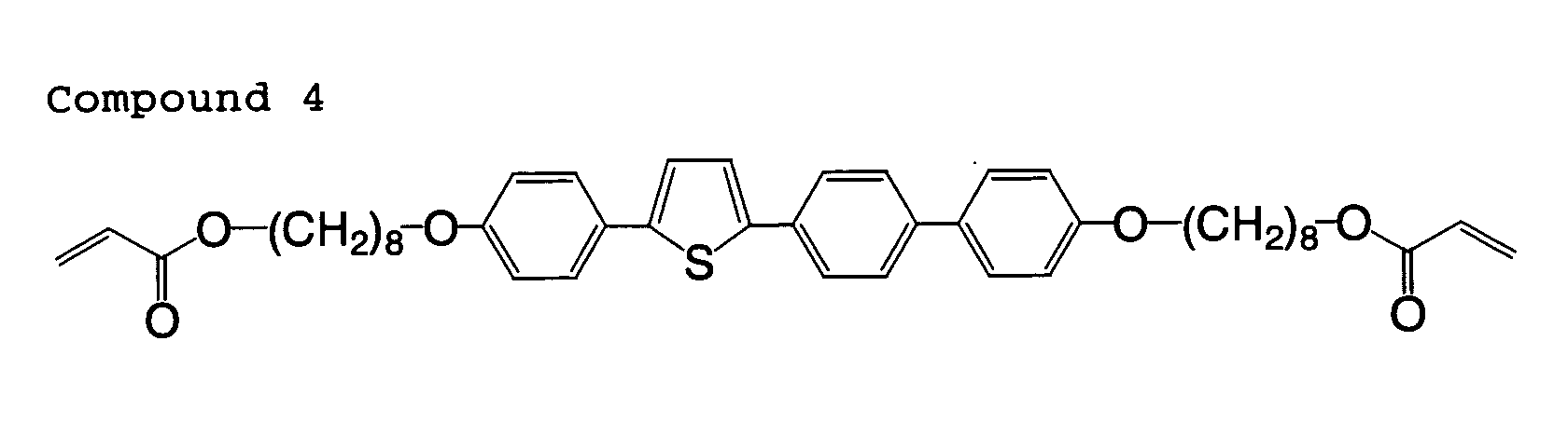
- Fig. 1 depicts a glass substrate 1A, a transparent electrode 2 and a light-emitting layer 3A, and the light-emitting layer 3A is formed by injecting a compound represented by the formula (1) or (2) (Compound 2) into a transparent electrode cell by a capillary force method and irradiating of a ultraviolet light.
- a compound represented by the formula (1) or (2) (Compound 2) Compound 2
- the transparent electrode 2 an ITO electrode formed by vapor deposition on the substrate 1A is preferred.
- the substrate 1A is a glass substrate and the transparent electrode 2 is an ITO electrode is most preferred.
- Fig. 2 is a schematic view showing a cross section of another embodiment of a light-emitting device according to the present invention.
- Fig. 2 depicts a flexible substrate 1B, a transparent electrode 2, a light-emitting layer 3B, and an orientation film 4A (orientation layer).
- the light-emitting layer 3B contains a polymer of a liquid crystalline compound, the polymeric medium described above, and glass beads, etc. as a spacer.
- the transparent electrode 2 is identical with that in Fig. 1.
- Fig. 3 is a schematic view showing a cross section of still another embodiment of a light-emitting device according to the invention.
- Fig. 3 depicts a glass substrate 1A, a transparent electrode 2, a light-emitting layer 3A, an orientation layer 4B, and a metal electrode 5.
- the glass substrate 1A, the transparent electrode 2 and the light-emitting layer 3A are identical with those in Fig. 1.
- Fig. 4 is a schematic view showing a cross section of a further embodiment of a light-emitting device according to the present invention.
- Fig. 4 depicts a glass substrate 1A, a transparent electrode 2, a hole transportation layer 7, a light-emitting layer 3A, an electron transportation layer 6, and a metal electrode 5.
- Fig. 5 is a schematic view showing a cross section of a still further embodiment of a light-emitting device according to the present invention.
- Fig. 5 depicts a glass substrate 1A, a transparent electrode 2, a light-emitting layer 3A, and an electron transportation layer 6.
- a light-emitting device shown in Fig. 1 was prepared as described below.
- the compound 2 was injected by a capillary force method in a cell in which 1.1 mm-thick glass plates which were each provided with ITO transparent electrodes of 30 nm thickness were arranged and bonded so as to face each other across a 2 ⁇ m gap therebetween(transparent electrode cell, manufactured by EHC Co.). Then, the cell was irradiated by a ultraviolet light (350 nm, 300 W) for 120 sec to prepare a crosslinked film.
- a ultraviolet light 350 nm, 300 W
- the device When a DC voltage (60 V) was applied to the ITO electrode, the device emitted light at a brightness of 10 cd/m 2 or more.
- a light-emitting device shown in Fig. 3 was prepared as described below.
- PEDOT/PSS poly-3,4-ethylenedioxy thiophene/polystyrene sulfonic acid
- the device When a DC voltage (11 V) was applied between the transparent ITO electrode and the aluminum electrode, the device emitted light at 440 cd/m 2 (room temperature). When the light emission intensity under room temperature and under heating at 80°C was compared, hardly any lowering of the emission strength due to heating was observed.
- the light-emitting device shown in Fig. 4 was prepared as described below.
- TPD N,N'-diphenyl-N,N'-di(m-tolyl)-benzidine
- the compound 2 to thickness of 30 nm
- Alq tris (8-hydroxyquinolinate) aluminum
- lithium fluoride to thickness of 5 nm on a glass plate of 1.1 mm thickness on which was formed a transparent ITO electrode of 30 nm thickness
- aluminum was vapor deposited to 500 nm to prepare a light-emitting device.
- a DC voltage 11 V
- the light-emitting device shown in Fig. 5 was prepared as described below.
- Two linear transparent ITO electrodes each of 30 nm thickness and 100 ⁇ m width was were formed (distance between the two linear transparent ITO electrodes: 10 ⁇ m) on a glass plate of 1.1 mm thickness.
- a 10 wt% chloroform solution of the compound 2 was spin coated on the substrate and dried sufficiently in vacuum. Then, when a voltage at 50 V was continuously applied between the two transparent ITO electrodes for 10 min, the device emitted a green light.
- the emission spectra in the horizontal direction and the vertical direction (with respect to the polarization axis) after passing through a polarization plate were as shown in Fig. 6.
- E1 is a plotted curve of the polarization brightness in the horizontal direction with respect to the polarization axis (vs wavelength)
- E2 is a plotted curve of the polarization brightness in the vertical direction with respect to the polarization axis (vs: wavelength).
- a light-emitting device which is stable with respect to heat, can be produced easily and, further, possesses excellent light emitting characteristics and polarization characteristics can be provided.
- the device can be manufactured without using a vapor deposition apparatus or the like and, hence, can be produced easily.
- the light-emitting layer is three dimensionally crosslinked and stable with respect to heat.
- a polarization light-emitting device can be prepared by fixing the liquid crystal orientation through crosslinking.
- a light-emitting layer can be disposed also between a pair of transparent electrodes, a both-side light-emitting body can be manufactured.
Landscapes
- Physics & Mathematics (AREA)
- Spectroscopy & Molecular Physics (AREA)
- Chemical & Material Sciences (AREA)
- Engineering & Computer Science (AREA)
- Materials Engineering (AREA)
- Electroluminescent Light Sources (AREA)
- Addition Polymer Or Copolymer, Post-Treatments, Or Chemical Modifications (AREA)
Abstract

Description


Claims (10)
- A light-emitting device comprising a layer formed from a compound represented by formula (1):wherein A represents a heterocyclic ring having at least one heteroatom, and Ar1 and Ar2 each independently represent an aromatic ring, provided that A, Ar1, and Ar2 each may have a substituent; B1 and B2 each independently represent a polymerizable substituent; C1 and C2 each independently represent a linear, branched, or cyclic linking group having 1 to 20 carbon atoms, and one or more -CH2- in the linking group may be substituted with -O-, -CO-, -NH-, -NR-, -CH=CH-, or -C ≡C- provided that the one or more -CH2- are not adjacent to a heteroatom; R represents an alkyl group having 1 to 20 carbon atoms, and one or more -CH2- in the alkyl group may be substituted with -O-, -CO-, -CH=CH-, or -C≡C- provided that the one or more -CH2- are not adjacent to a heteroatom; and n1 and n2 each independently represent an integer of 0, 1, or 2 provided that n1 and n2 do not both represent 0 at the same time.

- The device of claim 1, wherein A is selected from the group consisting of thiophene-2,5-diyl, thiazole-2,5-diyl, thiadiazole-2,5-diyl, pyridine-2,5-diyl, pyrimidine-2,5-diyl, pyrazine-2,5-diyl, and pyridazine-3,6-diyl.
- The device of claim 1, wherein A is thiophene-2,5-diyl or thiazole-2,5-diyl.
- The device in any one of claims 1 to 3, wherein Ar1 and Ar2 each independently represent 1,4-phenylene, 2,6-naphthalene, thiophene-2,5-diyl or thiazole-2,5-diyl.
- The device in any one of claims 1 to 4, wherein C1 and C2 each independently represent a linear alkyl group having 4 to 12 carbon atoms or a linear alkyloxy group.
- The device in any one of claims 1 to 5, wherein the compound represented by formula (1) is a compound represented by formula (2):wherein X represents a nitrogen atom or CH; Ar1 and Ar2 each independently represent an aromatic ring; B1 and B2 each independently represent a polymerizable substituent; n1 and n2 each independently represent an integer of 0, 1, or 2 provided that n1 and n2 do not both represent 0 at the same time; n3 and n4 each independently represent an integer from 1 to 20; D1 and D2 each independently represent a single bond, -O-, -COO-, -OCO-, -NH-, -NR-, -NRCO-, -CONR-, -NHCO-, or -CONH-; R represents an alkyl group having 1 to 20 carbon atoms, and one or more -CH2- in the alkyl group may be substituted with -O-, -CO-, -CH=CH-, or -C≡C- provided that the one or more -CH2- are not adjacent to a heteroatom; and B4 represents a single bond or an alkylene group having 2 to 10 carbon atoms which may be further substituted with an alkyl group.

- The device of claim 6, wherein Ar1 and Ar2 each independently represent 1,4-phenylene, 2,6-naphthalene, thiophene-2,5-diyl or thiazole-2,5-diyl.
- The device in any one of claims 1 to 7, wherein the compound represented by formula (1) is a compound exhibiting liquid crystallinity.
- The device in any one of claims 1 to 8, wherein the layer formed from the compound represented by formula (1) is provided between a pair of opposing transparent electrodes.
- The device of claim 9, wherein the layer formed from the compound represented by formula (1) is a layer formed by polymerization at a temperature where the compound represented by formula (1) exhibits liquid crystallinity and in a state where molecules of the compound represented by formula (1) are oriented uniaxially.
Applications Claiming Priority (2)
| Application Number | Priority Date | Filing Date | Title |
|---|---|---|---|
| JP2004051641A JP2005243432A (en) | 2004-02-26 | 2004-02-26 | Light-emitting element |
| JP2004051641 | 2004-02-26 |
Publications (2)
| Publication Number | Publication Date |
|---|---|
| EP1569287A2 true EP1569287A2 (en) | 2005-08-31 |
| EP1569287A3 EP1569287A3 (en) | 2008-11-26 |
Family
ID=34747510
Family Applications (1)
| Application Number | Title | Priority Date | Filing Date |
|---|---|---|---|
| EP05004110A Withdrawn EP1569287A3 (en) | 2004-02-26 | 2005-02-25 | Organic light emitting device materials and organic light emitting devices |
Country Status (2)
| Country | Link |
|---|---|
| EP (1) | EP1569287A3 (en) |
| JP (1) | JP2005243432A (en) |
Families Citing this family (4)
| Publication number | Priority date | Publication date | Assignee | Title |
|---|---|---|---|---|
| JP5689653B2 (en) | 2009-12-03 | 2015-03-25 | 富士フイルム株式会社 | Charge transport film, method for producing the same, light emitting device using the same, and photoelectric conversion device |
| JP5718023B2 (en) * | 2010-11-08 | 2015-05-13 | ユー・ディー・シー アイルランド リミテッド | Organic electroluminescent device and method for producing organic electroluminescent device |
| JP5981736B2 (en) * | 2011-04-12 | 2016-08-31 | ユー・ディー・シー アイルランド リミテッド | ORGANIC ELECTROLUMINESCENT ELEMENT, AND LIGHT EMITTING DEVICE, DISPLAY DEVICE AND LIGHTING DEVICE USING THE ORGANIC ELECTROLUMINESCENT ELEMENT |
| JP2016096097A (en) * | 2014-11-17 | 2016-05-26 | 大日本印刷株式会社 | Organic electroluminescent device |
Citations (3)
| Publication number | Priority date | Publication date | Assignee | Title |
|---|---|---|---|---|
| WO2003006468A2 (en) * | 2001-07-09 | 2003-01-23 | Merck Patent Gmbh | Polymerisable charge transport compounds |
| WO2004003108A1 (en) * | 2002-07-01 | 2004-01-08 | The University Of Hull | Luminescent compositions |
| EP1394158A1 (en) * | 2002-08-30 | 2004-03-03 | Fuji Photo Film Co., Ltd. | Novel compounds and optical elements using the same |
-
2004
- 2004-02-26 JP JP2004051641A patent/JP2005243432A/en active Pending
-
2005
- 2005-02-25 EP EP05004110A patent/EP1569287A3/en not_active Withdrawn
Patent Citations (3)
| Publication number | Priority date | Publication date | Assignee | Title |
|---|---|---|---|---|
| WO2003006468A2 (en) * | 2001-07-09 | 2003-01-23 | Merck Patent Gmbh | Polymerisable charge transport compounds |
| WO2004003108A1 (en) * | 2002-07-01 | 2004-01-08 | The University Of Hull | Luminescent compositions |
| EP1394158A1 (en) * | 2002-08-30 | 2004-03-03 | Fuji Photo Film Co., Ltd. | Novel compounds and optical elements using the same |
Also Published As
| Publication number | Publication date |
|---|---|
| EP1569287A3 (en) | 2008-11-26 |
| JP2005243432A (en) | 2005-09-08 |
Similar Documents
| Publication | Publication Date | Title |
|---|---|---|
| EP1805280B1 (en) | Carbazole derivative and organic light emitting device using same | |
| US8089064B2 (en) | Aromatic chalcogen compounds and their use | |
| EP2197979B1 (en) | Novel compound for organic photoelectric device and organic photoelectric device including the same | |
| JP3788676B2 (en) | Organic electroluminescent device material and organic electroluminescent device using the same | |
| US9601705B2 (en) | Material for organic electroluminescence element and organic electroluminescence element using the same, and method for manufacturing organic electroluminescence element | |
| JP5689653B2 (en) | Charge transport film, method for producing the same, light emitting device using the same, and photoelectric conversion device | |
| TWI434873B (en) | Mono-, oligo- and polymers of thienothiazole | |
| JP2002308855A (en) | New compound and luminescent element using the same | |
| JP5174517B2 (en) | Gas barrier film and organic device using the same | |
| JP2002255934A (en) | New compound, its polymer, light emission element material using these substances and the light emission element | |
| JP2002308837A (en) | New compound and light-emitting device using the same | |
| JP2007290369A (en) | Gas barrier laminated film, its manufacturing method and image display element | |
| EP1477993B1 (en) | Organic conductive material and conductive varnish | |
| CN105461685A (en) | Compound containing quinoxaline perssad and organic electroluminescence device of compound | |
| Chen et al. | Polarized electroluminescence from aligned chromophores by the friction transfer method | |
| EP1569287A2 (en) | Organic light emitting device materials and organic light emitting devices | |
| US20050189873A1 (en) | Lighting elements, devices and methods | |
| US20040126616A1 (en) | Polyester resin, functional device and organic electroluminescent device using polyester resin, and method of manufacturing organic electroluminescent device | |
| EP2408037A1 (en) | Organic light-emitting element material, organic light-emitting element, and process for producing same | |
| JP5718023B2 (en) | Organic electroluminescent device and method for producing organic electroluminescent device | |
| Kim et al. | Synergistic Enhancement of Luminescent and Ferroelectric Properties through Multi‐Clipping of Tetraphenylethenes | |
| JP2001288172A (en) | Material for organic light emission element, new heterocyclic compound and organic light emission element by using the same | |
| JP2000344780A (en) | New benzopyran compound, light emission element material and light emission element using the same | |
| US7261953B2 (en) | Organic electroluminescent device | |
| JP2005302641A (en) | Organic electroluminescent element, its manufacturing method, and electronic device |
Legal Events
| Date | Code | Title | Description |
|---|---|---|---|
| PUAI | Public reference made under article 153(3) epc to a published international application that has entered the european phase |
Free format text: ORIGINAL CODE: 0009012 |
|
| AK | Designated contracting states |
Kind code of ref document: A2 Designated state(s): AT BE BG CH CY CZ DE DK EE ES FI FR GB GR HU IE IS IT LI LT LU MC NL PL PT RO SE SI SK TR |
|
| AX | Request for extension of the european patent |
Extension state: AL BA HR LV MK YU |
|
| RAP1 | Party data changed (applicant data changed or rights of an application transferred) |
Owner name: FUJIFILM CORPORATION |
|
| PUAL | Search report despatched |
Free format text: ORIGINAL CODE: 0009013 |
|
| AK | Designated contracting states |
Kind code of ref document: A3 Designated state(s): AT BE BG CH CY CZ DE DK EE ES FI FR GB GR HU IE IS IT LI LT LU MC NL PL PT RO SE SI SK TR |
|
| AX | Request for extension of the european patent |
Extension state: AL BA HR LV MK YU |
|
| RIC1 | Information provided on ipc code assigned before grant |
Ipc: H01L 51/00 20060101AFI20081023BHEP |
|
| 17P | Request for examination filed |
Effective date: 20090401 |
|
| AKX | Designation fees paid |
Designated state(s): AT BE BG CH CY CZ DE DK EE ES FI FR GB GR HU IE IS IT LI LT LU MC NL PL PT RO SE SI SK TR |
|
| 17Q | First examination report despatched |
Effective date: 20100315 |
|
| STAA | Information on the status of an ep patent application or granted ep patent |
Free format text: STATUS: THE APPLICATION IS DEEMED TO BE WITHDRAWN |
|
| 18D | Application deemed to be withdrawn |
Effective date: 20100727 |