EP1569286A2 - Bistable molecular switches and associated methods - Google Patents
Bistable molecular switches and associated methods Download PDFInfo
- Publication number
- EP1569286A2 EP1569286A2 EP04019440A EP04019440A EP1569286A2 EP 1569286 A2 EP1569286 A2 EP 1569286A2 EP 04019440 A EP04019440 A EP 04019440A EP 04019440 A EP04019440 A EP 04019440A EP 1569286 A2 EP1569286 A2 EP 1569286A2
- Authority
- EP
- European Patent Office
- Prior art keywords
- molecular
- group
- state
- switches
- molecular switch
- Prior art date
- Legal status (The legal status is an assumption and is not a legal conclusion. Google has not performed a legal analysis and makes no representation as to the accuracy of the status listed.)
- Withdrawn
Links
Classifications
-
- B—PERFORMING OPERATIONS; TRANSPORTING
- B82—NANOTECHNOLOGY
- B82Y—SPECIFIC USES OR APPLICATIONS OF NANOSTRUCTURES; MEASUREMENT OR ANALYSIS OF NANOSTRUCTURES; MANUFACTURE OR TREATMENT OF NANOSTRUCTURES
- B82Y10/00—Nanotechnology for information processing, storage or transmission, e.g. quantum computing or single electron logic
-
- G—PHYSICS
- G02—OPTICS
- G02B—OPTICAL ELEMENTS, SYSTEMS OR APPARATUS
- G02B26/00—Optical devices or arrangements for the control of light using movable or deformable optical elements
- G02B26/02—Optical devices or arrangements for the control of light using movable or deformable optical elements for controlling the intensity of light
- G02B26/026—Optical devices or arrangements for the control of light using movable or deformable optical elements for controlling the intensity of light based on the rotation of particles under the influence of an external field, e.g. gyricons, twisting ball displays
-
- G—PHYSICS
- G02—OPTICS
- G02F—OPTICAL DEVICES OR ARRANGEMENTS FOR THE CONTROL OF LIGHT BY MODIFICATION OF THE OPTICAL PROPERTIES OF THE MEDIA OF THE ELEMENTS INVOLVED THEREIN; NON-LINEAR OPTICS; FREQUENCY-CHANGING OF LIGHT; OPTICAL LOGIC ELEMENTS; OPTICAL ANALOGUE/DIGITAL CONVERTERS
- G02F1/00—Devices or arrangements for the control of the intensity, colour, phase, polarisation or direction of light arriving from an independent light source, e.g. switching, gating or modulating; Non-linear optics
- G02F1/01—Devices or arrangements for the control of the intensity, colour, phase, polarisation or direction of light arriving from an independent light source, e.g. switching, gating or modulating; Non-linear optics for the control of the intensity, phase, polarisation or colour
- G02F1/17—Devices or arrangements for the control of the intensity, colour, phase, polarisation or direction of light arriving from an independent light source, e.g. switching, gating or modulating; Non-linear optics for the control of the intensity, phase, polarisation or colour based on variable-absorption elements not provided for in groups G02F1/015 - G02F1/169
- G02F1/174—Devices or arrangements for the control of the intensity, colour, phase, polarisation or direction of light arriving from an independent light source, e.g. switching, gating or modulating; Non-linear optics for the control of the intensity, phase, polarisation or colour based on variable-absorption elements not provided for in groups G02F1/015 - G02F1/169 based on absorption band-shift, e.g. Stark - or Franz-Keldysh effect
-
- G—PHYSICS
- G11—INFORMATION STORAGE
- G11C—STATIC STORES
- G11C13/00—Digital stores characterised by the use of storage elements not covered by groups G11C11/00, G11C23/00, or G11C25/00
- G11C13/0002—Digital stores characterised by the use of storage elements not covered by groups G11C11/00, G11C23/00, or G11C25/00 using resistive RAM [RRAM] elements
- G11C13/0009—RRAM elements whose operation depends upon chemical change
- G11C13/0014—RRAM elements whose operation depends upon chemical change comprising cells based on organic memory material
-
- G—PHYSICS
- G11—INFORMATION STORAGE
- G11C—STATIC STORES
- G11C23/00—Digital stores characterised by movement of mechanical parts to effect storage, e.g. using balls; Storage elements therefor
-
- H—ELECTRICITY
- H10—SEMICONDUCTOR DEVICES; ELECTRIC SOLID-STATE DEVICES NOT OTHERWISE PROVIDED FOR
- H10K—ORGANIC ELECTRIC SOLID-STATE DEVICES
- H10K10/00—Organic devices specially adapted for rectifying, amplifying, oscillating or switching; Organic capacitors or resistors having potential barriers
- H10K10/701—Organic molecular electronic devices
-
- H—ELECTRICITY
- H10—SEMICONDUCTOR DEVICES; ELECTRIC SOLID-STATE DEVICES NOT OTHERWISE PROVIDED FOR
- H10K—ORGANIC ELECTRIC SOLID-STATE DEVICES
- H10K85/00—Organic materials used in the body or electrodes of devices covered by this subclass
- H10K85/60—Organic compounds having low molecular weight
-
- G—PHYSICS
- G11—INFORMATION STORAGE
- G11C—STATIC STORES
- G11C13/00—Digital stores characterised by the use of storage elements not covered by groups G11C11/00, G11C23/00, or G11C25/00
-
- G—PHYSICS
- G11—INFORMATION STORAGE
- G11C—STATIC STORES
- G11C2213/00—Indexing scheme relating to G11C13/00 for features not covered by this group
- G11C2213/10—Resistive cells; Technology aspects
- G11C2213/14—Use of different molecule structures as storage states, e.g. part of molecule being rotated
-
- G—PHYSICS
- G11—INFORMATION STORAGE
- G11C—STATIC STORES
- G11C2213/00—Indexing scheme relating to G11C13/00 for features not covered by this group
- G11C2213/70—Resistive array aspects
- G11C2213/77—Array wherein the memory element being directly connected to the bit lines and word lines without any access device being used
Definitions
- the present invention relates generally to molecular electronic switches. More particularly, the present invention relates to specific classes of compounds which are bistable and suitable for production of electronic devices such as ROM memory and the like.
- rotaxanes provide an irreversible switch that can only be toggled once. Thus, it can be suitable for use in a programmable read-only memory (PROM) device; however, it is unsuitable for use in reconfigurable devices. Further, rotaxanes are complex molecules which tend to be relatively large. As a result, the switching times of these molecules can be slow. In addition, rotaxanes require an oxidation and/or reduction reaction to occur before the switch can be toggled. With respect to catenane switches, the primary concerns are the small ON-to-OFF ratio and slow switching times.
- a bistable molecular switch can have a highly conjugated first state and a less conjugated second state.
- the bistable molecular switch can be configured such that application of an electric field reversibly switches the molecular switch from the first state to the second state.
- the bistable molecular switch can include a hydrophobic moiety and a hydrophilic moiety.
- the molecular switches can be used in a method for storing data.
- a molecular switch system can be formed which can include a layer of molecular switches between a first electrode layer and a second electrode layer.
- the layer of molecular switches can have substantially all of the molecular switches having their hydrophilic moiety oriented in the same direction.
- An electric potential can then be induced between the first and second electrode layers sufficient to switch the molecular switches from the first or second state to the second or first state, respectively.
- bistable refers to a property of a molecule such that the molecule has at least two relatively low energy states separated by an activation barrier.
- the molecule can be independently stable in either of the two low energy states.
- reversibly refers to a process of change in condition which is not permanent and can be undone to return to an original condition.
- reversibly switching a molecule can involve changing a molecular configuration from a first state to a second state. The molecule can subsequently be reversibly switched from the second state to the original first state.
- conjugated refers to the degree of ⁇ -bonding electrons in a molecule.
- a highly conjugated molecule has a relatively high number of electrons occupying ⁇ bonds.
- Such conjugated molecules are also characterized by a delocalization of electrons over at least a portion of the molecule.
- monolayer refers to a layer of molecules which has a thickness of a single molecule.
- a monolayer can cover almost any area and has a thickness of one molecule substantially over the entire area.
- defects can be present in such monolayers and such defects are acceptable, as long as the desired properties are maintained.
- self-assembly refers to a process wherein a system, i.e. plurality of molecules, naturally adopts a regular pattern and orientation of individual molecules based on the conditions and molecules involved.
- substituted refers to a compound having a carbon and/or hydrogen replaced by a heteroatom or functional group.
- dipole moment refers to any charge separation which is associated with uneven electron distributions within a molecule or portion thereof and can be described by a vector.
- the term should also be interpreted to cover multipole moments, e.g., quadrupoles, octopoles, etc.
- ⁇ -bonding electrons refers to electrons which occupy orbitals associated with ⁇ bonds, whether pure ⁇ bonds or hybridized bonds, e.g., ⁇ - ⁇ bonds.
- a size range of about 1 ⁇ m to about 200 ⁇ m should be interpreted to include not only the explicitly recited limits of 1 ⁇ m and about 200 ⁇ m, but also to include individual sizes such as 2 ⁇ m, 3 ⁇ m, 4 ⁇ m, and sub-ranges such as 10 ⁇ m to 50 ⁇ m, 20 ⁇ m to 100 ⁇ m, etc.
- a bistable molecular switch can have a highly conjugated first state and a less conjugated second state.
- the molecular switch In the highly conjugated first state, the molecular switch is typically conductive, while in the less conjugated second state the molecular switch is less conductive.
- Application of an electric field can reversibly switch the molecular switch from the first state to the second state or from the second state to the first state, depending on the direction of the applied electric field.
- Molecular switches of the present invention can typically include a hydrophobic moiety and a hydrophilic moiety.
- reversible switching can be accomplished using electric field induced rotation of a portion of the molecular switch sufficient to change the band gap, i.e. conductivity, of the molecular switch.
- reversible switching can be realized using electric field induced rearrangement of bonding sufficient to cause a change in band gap.
- intramolecular bonds can be formed and/or broken which allow for a reversible change in the conjugation of the molecule.
- reversible switching can be achieved using electric field induced intramolecular folding and/or stretching.
- the molecular switch can include at least one rotor, which is a portion of the molecular switch that can rotate or otherwise change position with respect to the balance of the molecular switch molecule.
- Each rotor can have a donor group and an acceptor group, each of which is operably connected thereto.
- the rotor can be connected to at least one stator and preferably between two stators such that rotation of the rotor is permitted with respect to the stators.
- Stators are typically relatively stationary moieties that can contribute to providing an axis for the rotor to rotate or change position.
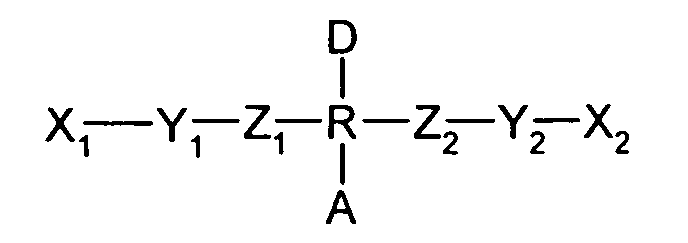
- the molecular switches of the present invention can have the general molecular structure of Formula I, as follows: where A is an acceptor group, D is a donor group, R is a rotor, X 1 is a hydrophilic moiety, X 2 is a hydrophobic moiety, Y 1 is a first stator, Y 2 is a second stator, Z 1 is a first bridging group, and Z 2 is a second bridging group. Additional optional groups can also be included between the bridging groups and stators, and/or the rotor, hydrophilic moiety, and hydrophobic moiety. Alternatively, some of these components can be merged into single components, such as where a bridging group is part of one of the stators or the rotor, for example. Each of the groups described in Formula I above is discussed in more detail below.
- Suitable rotor groups can have a variety of configurations. However, as a general guideline, rotors can be planar groups having at least some electrons available for ⁇ -bonding orbitals. In one embodiment, a rotor can be aromatic or heterocyclic.
- suitable rotors can include, without limitation, benzene or substituted benzene, naphthalene, acenaphthalene, anthracene, phenanthrene, benzanthracene, dibenzanthracene, fluorene, benzofluorene, fluoranthene, pyrene, benzopyrene, naphthopyrene, chrysene, perylene, benzoperylene, pentacene, coronene, tetraphenylene, triphenylene, decacyclene, pyrrole, thiophene, porphine, pyrazole, imidazole, triazole, isoxazole, oxadiazole, thiazole, isothiazole, thiadiazole, pyridazine, pyrimidine, uracil, azauracil, pyrazine, triazine, pyridine, indole
- the rotor can have at least one acceptor group and at least one donor group connected such that the A-R-D portion of Formula I has a relatively large dipole moment.
- the A-R-D portion of the molecular switch can rotate in an attempt to align the dipole moment parallel with the electric field.
- the magnitude of the dipole moment can be largely determined by the relative difference in electronegativity of the acceptor and donor groups.
- the donor group can have a lower electronegativity than the acceptor group in order to produce an A-R-D rotor segment having a relatively large dipole moment.
- the acceptor and donor groups can be operably connected to the rotor in any number of configurations. Any functional configuration can be used, as long as the A-R-D rotor segment has a large dipole moment.
- the acceptor and donor groups can be attached to the rotor directly opposite each other.
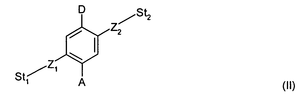
- Formula II shows a molecular switch having a phenyl rotor with the acceptor and donor groups that are positioned para, as shown below: where St 1 and St 2 represent the stators in combination with the hydrophilic and hydrophobic moieties, respectively, and Z 1 , Z 2 , A, and D are defined as described in Formula I.
- the electric field can be applied substantially perpendicular to a molecular axis defined along a line between St 1 and St 2 .
- the electric field can be applied from about a 45° to about a 90° angle with respect to the molecular axis. Therefore, the dipole moment and electric field can be offset in some embodiments.
- the acceptor and donor groups can be attached at various positions on the rotor.
- the acceptor and donor groups can be attached to a phenyl rotor such that the groups are positioned meta with respect to one another. In short, almost any configuration where the dipole moment can cause motion of the rotor under the applied electric field can be operable.
- steric or Coulombic repulsion can prevent the rotor from rotating a full 180°.
- the rotor and stators, along with any other portions of the molecular switch have electrons delocalized, or shared, over a large portion of the molecular switch.
- This first state is typically associated with rotor and stators in a coplanar orientation.
- the rotor is not coplanar with the stators.
- conjugation is segregated to various portions of the molecular switch.
- the ⁇ -bonding electrons are segregated separately in the rotor and each stator in the second state.
- the donor group can be any group which is electron donating in a given environment.
- suitable donor groups include a hydrocarbon having from one to six carbon atoms, hydrogen, amine, hydroxy, thiol, ether, and combinations thereof.
- the donor group can be a functional group containing at least one heteroatom selected from the group consisting of B, Si, I, N, O, S, and P. In one embodiment, the donor group can be methyl.
- the acceptor group can be any group which is electron withdrawing in the given environment. Suitable acceptor groups can include, but are not limited to, nitro, nitrile, hydrogen, acids, ketone, imine, trifluoromethyl, trichloromethyl, hydrocarbons having from one to six carbon atoms, and combinations thereof. Additionally, the acceptor group can be heteroatoms selected from the group consisting of N, O, S, P, F, Cl, and Br, or functional groups having at least one of such heteroatoms, e.g., OH, SH, NH, and the like. In one specific embodiment, the acceptor group can be nitro.
- the above listed donor and acceptor groups are merely exemplary and those skilled in the art can choose other appropriate groups based on the description herein. Further, the specific donor and acceptor groups are not as important as the relative differences in electronegativity. This is why several groups listed can be either a donor or acceptor group depending on the other group attached to the rotor.
- One basic consideration in choosing appropriate donor and acceptor groups is that the donor group has a lower electronegativity than the acceptor group sufficient to create a large dipole moment across the rotor. In some embodiments of the present invention, the large dipole moment can be from about 3 Debye (D) to about 30 D, and can typically range from about 4 D to about 6 D.
- bridging groups can be connected between the rotor and stators, as shown in Formula I. Suitable bridging groups can have at least one bond about which rotation can occur. Additionally, bridging groups having available ⁇ -bonding electrons can further increase the overall conjugation of the molecular switch.
- the bridging groups can be acetylene, ethylene, amide, imide, imine, azo, and combinations thereof. In one specific embodiment, the bridging groups can each be acetylene. Alternatively, as described previously, bridging groups can be part of or provided by either the rotor or stators.
- the stators can be of any group which is configured to substantially maintain its position relative to the rotor during rotation of the rotor.
- Suitable stators can include conjugated rings, aromatic rings, and saturated, unsaturated, or substituted hydrocarbons.
- stators can include rings which have ⁇ -bonding electrons available to contribute to the overall conjugation of the molecular switch.
- stators can be independently selected from groups such as benzene or substituted benzene, phenyl, naphthalene, acenaphthalene, anthracene, phenanthrene, benzanthracene, dibenzanthracene, fluorene, benzofluorene, fluoranthene, pyrene, benzopyrene, naphthopyrene, chrysene, perylene, benzoperylene, pentacene, coronene, tetraphenylene, triphenylene, decacyclene, pyrrole, thiophene, porphine, pyrazole, imidazole, triazole, isoxazole, oxadiazole, thiazole, isothiazole, thiadiazole, pyridazine, pyrimidine, uracil, azauracil, pyrazine, triazine
- One difficulty with molecular switches can be related to the orientation of individual molecules in a useful direction with respect to an electric field and/or associated electrodes.
- hydrophobic and hydrophilic groups can be attached at either end of the molecular switch. Forming molecular switches each having a hydrophilic and a hydrophobic moiety allows for arrangement of individual molecules using thin film techniques such as self-assembly techniques, Langmuir-Blodgett techniques, and the like.
- the hydrophobic moiety suitable for use in the molecular switches can include any functional hydrophobic group.
- Suitable hydrophobic moieties can include long substituted or unsubstituted hydrophobic chains having from 6 to about 30 carbons.
- the hydrophobic moiety can be a long substituted or unsubstituted hydrophobic chain having from 8 to about 20 carbons.
- Specific non-limiting examples of hydrophobic moieties for use with the present invention include alkyl, alkoxy, alkyl thio, alkyl seleno, alkyl amino, aryl, aryloxy, aryl thio, aryl seleno, aryl amino, and the like.
- the hydrophobic moiety can be an unsubstituted alkyl.
- the molecular switches of the present invention can have a plurality of hydrophobic moieties.
- the hydrophobic moiety can be selected to create a protective layer between the rotor and an electrode. This protective layer can provide chemical and mechanical protection to the stator and rotor portions of the molecular switches. This can be particularly helpful during construction of an operable molecular switch system, described in more detail below. Such construction often involves processes such as metal deposition, which may damage unprotected stators and/or rotors. Hydrophobic moieties which provide such protection can typically form a protective layer from about 1 nm to about 4 nm in thickness.
- hydrophilic moiety can be used in the molecular switches of the present invention.
- the hydrophilic moiety can be selected to form a bond, e.g., chemical, mechanical, or electrostatic, between the switchable molecule and a substrate, such as an electrode.
- Hydrophilic moieties can typically form a protective layer from about 0.1 nm to about 1.5 nm in thickness.
- hydrophilic moieties include carboxylic acids, alcohols, amines, thiols, sulfonic acids, sulfuric acid, ethyl, ethers or polyethers, tetrahydrofurans, pyridines, imidazoles, pyrroles, furans, thiophenes, and the like.
- the hydrophilic moiety can be carboxylate.
- the molecular switches of the present invention can have a plurality of hydrophilic moieties.
- Formula IV depicts one currently useful class of molecular switches in accordance with the principles of the present invention, as shown below: where n is an integer from 5 to about 29.
- the hydrophilic and/or hydrophobic moieties can be supplied as part of the stators.
- phenyl can act as both a stator and a hydrophobic moiety.
- the molecular switches can be assembled to form a molecular switch system.
- the molecular switch system can include a substrate and a plurality of bistable molecular switches on the substrate.
- the molecular switch system preferably has substantially all of the molecular switches oriented such that the hydrophilic moieties are oriented in the same direction.
- the molecular switches can be arranged having their hydrophilic moieties oriented in the same direction.
- suitable thin film preparation methods can include, without limitation, Langmuir-Blodgett (L-B), self-assembly mechanisms (SAM), vapor phase deposition, or the like.
- the molecular switches can be suspended in a solvent based solution which is then thick film coated onto a substrate, e.g., reverse rolling, spin-coated onto a substrate, or dried while being subjected to an electric field that orients the molecules.
- the thin film method used can allow formation of a monolayer of molecular switches.
- any method that can produce a substantially monolayer thin film where a molecular axis is defined by an axis between the hydrophobic and hydrophilic moieties, and is oriented substantially parallel with the electric field that will be applied, can be suitable for use in the present invention.
- Typical L-B film methods and self-assembly methods can provide a very high concentration of molecular switches per area.
- the molecular switches can be formed in a monolayer at concentrations of about 10 6 molecules per square micron to about 10 7 molecules per square micron.
- the molecular switches can be arranged using a SAM technique.
- the molecular switches can be arranged using Langmuir-Blodgett (L-B) films.
- L-B film techniques are well known to those skilled in the art.
- L-B methods involve placing a measured amount of material having hydrophobic groups and hydrophilic groups on a fluid surface. The material forms a monolayer at the surface with the hydrophilic groups oriented in the same direction.
- the fluid can typically be water; however, other materials can be used, e.g., glycerine, mercury, etc. If water is used, then the hydrophilic ends are oriented in the water, while the hydrophobic ends are oriented away from the water surface. Alternatively, a hydrophobic material can be used such that the hydrophobic end is oriented toward the hydrophobic material and the hydrophilic end is oriented away from the hydrophobic material.
- a first substrate can then be passed through the monolayer, wherein the molecules transfer to the substrate as a monolayer.
- the substrate can have either a hydrophilic or hydrophobic surface.
- hydrophilic substrates can be passed through the monolayer from the water side, while hydrophobic substrates can typically be passed through the monolayer from above the monolayer. Passing a hydrophilic substrate through the monolayer can result in the molecular switches oriented with the hydrophilic ends toward the substrate and the hydrophobic ends oriented away from the substrate. Similarly, passing a hydrophobic substrate through the monolayer results in the hydrophilic ends oriented away from the substrate.
- the molecular switch systems of the present invention can include forming either a single monolayer of molecular switches or a plurality of monolayers.
- the L-B method is well suited for the formation of either a single monolayer or multiple stacked monolayers. When multiple monolayers are formed, the hydrophilic ends of the molecular switches can substantially all become oriented in a common same direction.
- the first substrate having a monolayer thereon can be passed through an L-B film to deposit additional monolayers on the surface. Multiple passes of a hydrophilic substrate can be referred to as Z-type deposition, whereas multiple passes of a hydrophobic substrate can be referred to as Y-type deposition.
- Suitable hydrophilic substrates can include, without limitation, silver, gold, copper, chromium, aluminum, tin, tin oxides, glass, quartz, silicon, gallium arsenide, and alloys thereof.
- the first substrate can be formed of a conductive metal such as silver, gold, copper, or the like.
- Suitable hydrophobic substrates can include, without limitation, etched silicon, mica, highly ordered pyrolytic graphite (HOPG), or the like.
- the substrates of the present invention can be hydrophilic substrates.
- the first substrate can be a conductive layer suitable for use as an electrode.
- the substrate can comprise a transparent or translucent material. Such transparent materials can be suitable for use in producing heads-up displays or other see-through devices.
- the molecular switch system can further include a second substrate opposite the first substrate such that the plurality of molecular switches are between the first and second substrates.
- the second substrate can be formed using any number of known deposition techniques. Several non-limiting examples of suitable deposition techniques include physical vapor deposition, electrodeposition, electroless deposition, and the like.
- the second substrate can be formed of a variety of materials, depending on the desired application.
- the second substrate can be formed of the same or of a different material than the first substrate.
- suitable substrate materials include metals, metal oxides, metal alloys, glass, quartz, mica, HOPG, or the like.
- the second substrate can be formed of silver, gold, copper, platinum, chromium, aluminum, glass, quartz, silicon, gallium arsenide, ITO, or alloys thereof.
- the second substrate can typically be a conductive electrode layer comprising a conductive metal or alloy such as silver, gold, copper, alloys thereof, or the like.
- the first and second substrates can be almost any practical thickness, depending on the intended application.
- the molecular switch system of the present invention can include substrates having a thickness of from 1 nm to about 1.5 ⁇ m, though thickness up to 500 ⁇ m can be used.
- the specific molecular switches used can affect the total thickness of the molecular switch system.
- the layer of molecular switches can have a thickness of from about 1 nm to about 100 nm, depending on the number of monolayers and the specific molecular switch structure. In embodiments having a single monolayer of molecular switches, the layer of molecular switches can have a thickness of from about 1 nm to about 10 nm.
- the layer of molecular switches can have a thickness of from about 1.5 nm to about 5 nm. In one detailed embodiment of the present invention, the entire molecular switch system can have a thickness of from about 1 nm to about 100 mm.
- the layer of molecular switches can cover an entire substrate surface or merely a portion thereof, depending on the intended application. For example, it can be desirable to deposit molecular switches over a portion of a substrate in order to leave room for additional components formed by subsequent processing, such as by photolithographic exposure or the like.
- the layer of molecular switches can cover an area of the substrate of from about 0.01 ⁇ m 2 to about 0.01 mm 2 , although areas outside this range can be used, depending on the application. For example, areas up to 1 cm 2 and beyond are possible.
- Those skilled in the art can design specific electronic structures and devices based on the disclosure herein to thus incorporate the molecular switches of the present invention into a variety of devices.
- a molecular switch system including a layer of molecular switches between a first electrode layer and a second electrode layer, can be formed as discussed above. With substantially all of the hydrophilic moieties oriented in the same direction, application of an electric potential across the electrode layers can have a relatively uniform effect on individual molecular switches. Typically, inducing an electric potential between the first and second electrode layers can be sufficient to switch the molecular switches from the first or second state to the second or first state, respectively. Recall that the first state is the highly conjugated state, while the second state is less conjugated.
- Formula V illustrates an exemplary situation with respect to a single molecular switch within a monolayer, as follows:
- Formula V shows the rotor having rotated 90°; however, this is merely an idealized rotation shown for exemplary purposes, as actual angles of rotation can vary somewhat as discussed earlier.
- the actual angle of rotation can depend on the specific acceptor and donor groups, associated steric interactions, i.e. including intermolecular and intramolecular forces, applied electric field strength, temperature, and the like. More generally, for the molecular switch of Formula V, the angle of rotation can vary from about 30° to about 150°. In addition, the rotation of the rotor is typically not acting alone without other outside influences.
- the single bistable molecule shown in Formula V is part of a large number of molecular switches that form a monolayer.
- Other similar bistable monolayers are oriented generally parallel with respect to the depicted single molecule to form a plane of molecules along an approximate z-axis with respect the molecule shown.
- directly above and below the plane of molecules can be other planes of molecules that are oriented along a y-axis with respect to the plane of molecules described previously.
- the term "plane" is not intended to infer that these molecules are perfectly aligned in rigid planar structures, but that the plurality of molecules is generally organized in a monolayer between the electrode layers.
- the electric potential can vary in field strength depending on the specific molecular switch and the number of monolayers included. Typically, the electric potential can be from about 1 ⁇ V to about 1000 ⁇ V per molecular switch. The electric potential does not need to be maintained once the molecular switch has switched from one state to the other. Most often, the molecular switches of the present invention can be switched relatively quickly. In some embodiments of the present invention, the electric potential can be applied for about 1 ⁇ sec to about 10 msec. Note that each state is stable, thus the electric field does not need to be maintained in order to preserve either the first or second state once the switch has been placed in the first or second position. Further, the electric field can be applied along the molecular axis or at any other functional direction.
- the electric field used to rotate the rotor can be independent of the electric field across the molecular switch.
- the electric field can be applied in any direction such that rotation of the rotor occurs sufficient to switch the molecular switch from the first state to the second state or from the second state to the first state.
- the first state can be highly conjugated, which allows for free movement of electrons across substantially the entire molecular switch.
- the second state can be less conjugated wherein conjugation and ⁇ -bonding electrons are segregated to portions of the molecule.
- the conjugation is segregated to at least three portions, i.e. the two phenyl stators and the phenyl rotor.
- the first state can have a first resistivity (R 1 )
- the second state can have a second resistivity (R 2 ).
- the ratio of R 2 /R 1 illustrates the difference in resistivity between the two states and can be one measure of the ability of a molecular switch to act as useful electronic components.
- the ratio of R 2 /R 1 can be from about 10 to about 100, and in another aspect can be from about 2 to about 10 4 .
- the molecular switches described herein can be assembled to form any number of electronic components such as cross-bar and other circuits.
- Cross-bar circuits can be formed to perform memory, logic, communication, and other functions.
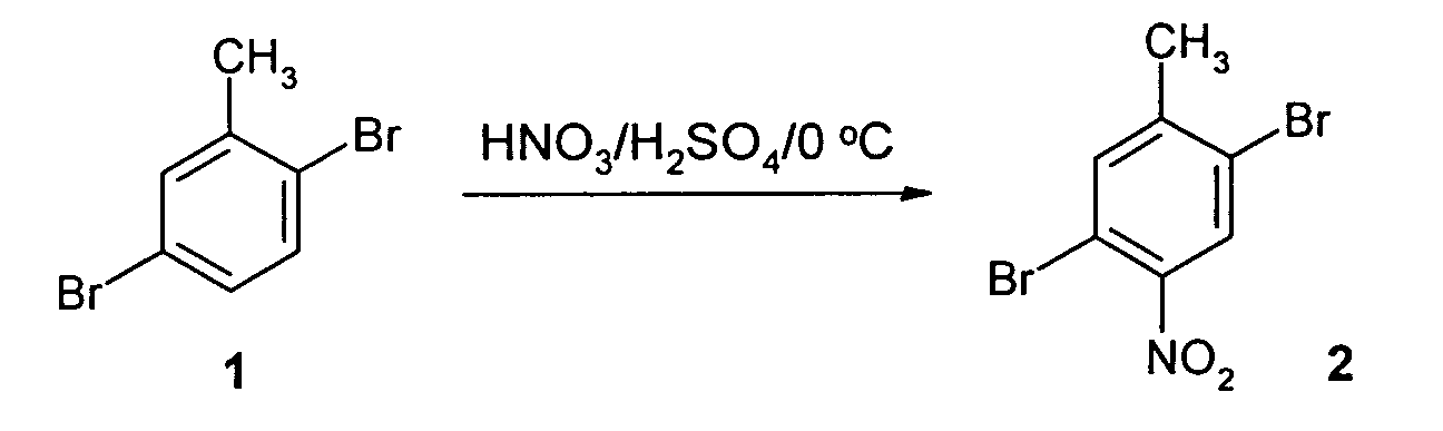
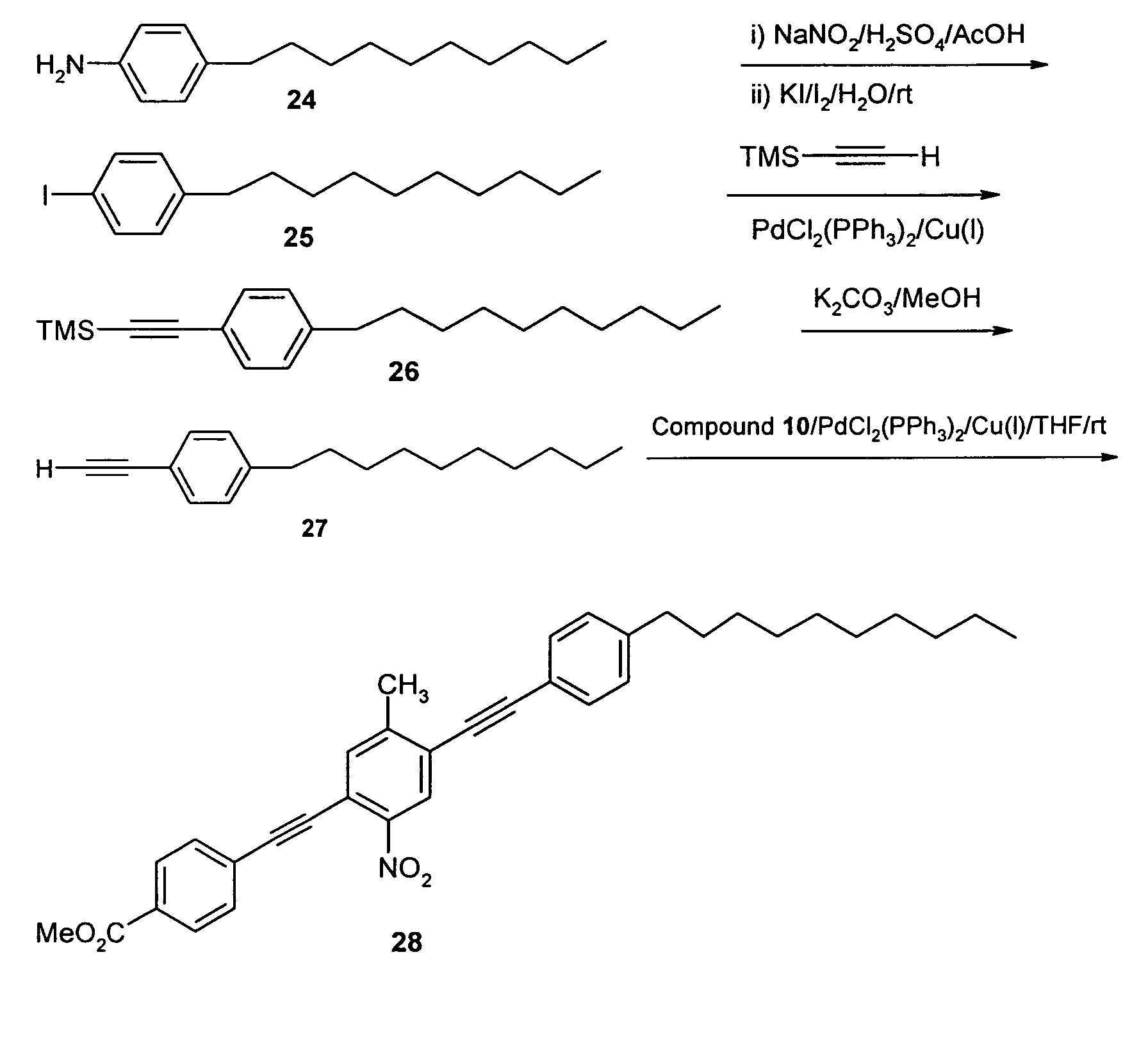
- Nitration of readily available 2,5-dibromotoluene (1) was performed by mixing excess nitric acid and sulfuric acid at about 0 °C for 30 minutes, as shown below.
- the product 2,5-dibromo-4-nitrotoluene (2) was achieved with a 60% yield as a pale yellow solid.
- the nitro substituent provides a strong electron-withdrawing group, i.e. the acceptor group, while methyl acts as a donor group.
- Compound 2 was then used as a reactant for attachment of the rotor portion of a molecular switch.
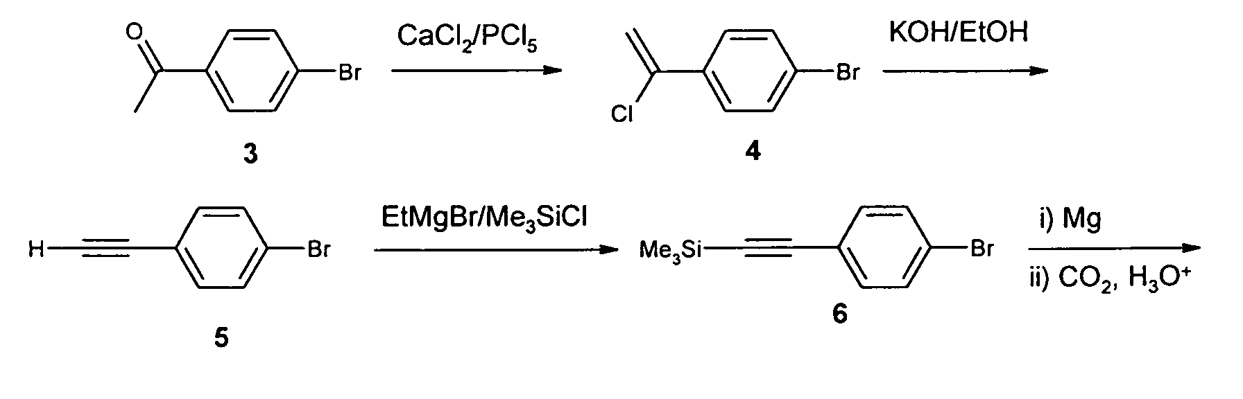
- 4-bromoacetophenone (3) can be treated with powdered phosphorous pentachloride to produce 1-(4-bromophenyl)-1-chloroethylene (4).
- Compound 4 was then treated with potassium hydroxide to produce 4-bromophenylacetylene (5) at a 60% yield.
- Treatment of compound 5 with ethyl magnesium bromide was followed by reaction with chlorotrimethylsilane.
- the resulting product (4-bromophenylethynyl) trimethylsilane (6) was recovered with a 90% yield.
- Compound 6 was then treated with ethyl magnesium bromide, followed by reaction with carbon dioxide to produce (4-carboxyphenylethynyl) trimethylsilane (7) in 89% yield.
- Compound 7 was then deprotected using KOH in methanol to form 4-ethynylbenzoic acid (8) in 96% yield.
- Compound 8 is a useful building block for forming a variety of molecular switches in accordance with the present invention, and was used in forming molecular switches of the following examples.
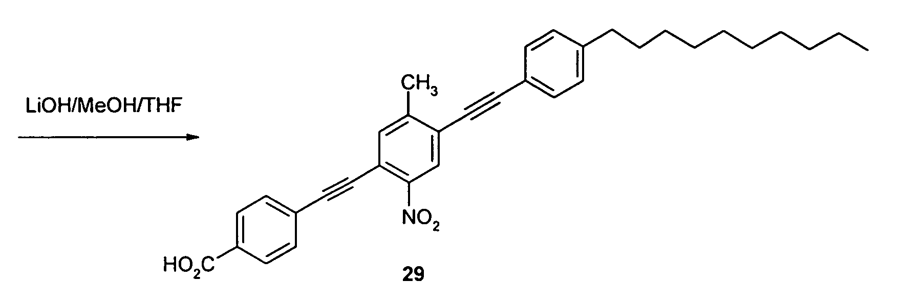
- reaction sequence shown below was used to produce a molecular switch having a decyl group as the hydrophobic moiety and a carboxy group as the hydrophilic moiety.
- Molecular switch 29 includes a decyl group as the hydrophobic moiety and a carboxy group as the hydrophilic moiety which is stable and well suited to monolayer formation using L-B methods.
Landscapes
- Physics & Mathematics (AREA)
- Engineering & Computer Science (AREA)
- Chemical & Material Sciences (AREA)
- Nonlinear Science (AREA)
- General Physics & Mathematics (AREA)
- Optics & Photonics (AREA)
- Spectroscopy & Molecular Physics (AREA)
- Nanotechnology (AREA)
- Crystallography & Structural Chemistry (AREA)
- Theoretical Computer Science (AREA)
- Health & Medical Sciences (AREA)
- Life Sciences & Earth Sciences (AREA)
- Molecular Biology (AREA)
- Mathematical Physics (AREA)
- Materials Engineering (AREA)
- Semiconductor Memories (AREA)
- Electroluminescent Light Sources (AREA)
Abstract
Description


Claims (17)
- A bistable molecular switch having a highly conjugated first state and a less conjugated second state such that application of an electric field reversibly switches the molecular switch from the first state to the second state, said molecular switch comprising a hydrophobic moiety and a hydrophilic moiety.
- The molecular switch of claim 1, further comprising at least one rotor having a donor group and an acceptor group, each of the donor and the acceptor groups being operably connected to the rotor to cause switching upon application of an electric field, said donor group having a lower electronegativity than the acceptor group.
- The molecular switch of claim 2, wherein said molecular switch has the general molecular structurewhere A is the acceptor group, D is the donor group, R is the rotor, X1 is the hydrophilic moiety, X2 is the hydrophobic moiety, Y1 is a first stator, Y2 is a second stator, Z1 is a first bridging group, and Z2 is a second bridging group.

- The molecular switch of claim 3, wherein the hydrophobic moiety comprises a long substituted or unsubstituted hydrophobic chain having from 6 to about 30 carbons.
- The molecular switch of claim 3, wherein the hydrophobic moiety comprises a member selected from the group consisting of alkyl, alkoxy, alkyl thio, alkyl amino, alkyl seleno, aryl, aryloxy, aryl thio, aryl amino, aryl seleno, and combinations thereof.
- The molecular switch of claim 3, wherein the hydrophilic moiety is selected from the group consisting of carboxylic acid, sulfuric acid, alcohol, ethyl, polyether, tetrahydrofuran, pyridine, imidazole, pyrrole, furan, thiophene, and combinations thereof.
- The molecular switch of claim 3, wherein the donor group is selected from the group consisting of a hydrocarbon having from one to six carbon atoms, hydrogen, amine, hydroxy, thiol, ether, and combinations thereof.
- The molecular switch of claim 7, wherein the acceptor group is selected from the group consisting of nitro, nitrile, ketone, imine, acids, trifluoromethyl, trichloromethyl, hydrocarbons having from one to six carbon atoms, and combinations thereof, and wherein said donor group has a lower electronegativity than the acceptor group.
- A molecular switch system, comprising:wherein said molecular switch has a hydrophobic moiety and a hydrophilic moiety such that substantially all of the molecular switches have the hydrophilic moiety oriented in the same direction, wherein said molecular switches each further comprise at least one rotor having a donor group and an acceptor group each operably connected to the rotor to cause switching upon application of an electric field, said donor group having a lower electronegativity than the acceptor group and wherein said molecular switch has the general molecular structurea) a substrate; andb) a plurality of bistable molecular switches on the substrate, said molecular switches having a highly conjugated first state and a less conjugated second state such that application of an electric field reversibly switches the molecular switch from the first state to the second state, andwhere A is the acceptor group, D is the donor group, R is the rotor, X1 is the hydrophilic moiety, X2 is the hydrophobic moiety, Y1 is a first stator, Y2 is a second stator, Z1 is a first bridging group, and Z2 is a second bridging group.

- The system of claim 9, wherein the substrate is a conductive electrode layer.
- The system of claim 10, further comprising a second conductive electrode layer such that the plurality of molecular switches are between the conductive electrode layer and second conductive electrode layer.
- The system of claim 9, wherein the substrate has a thickness of from 1 nm to about 1.5 µm.
- The system of claim 9, wherein the plurality of molecular switches are configured in a single monolayer.
- A method of storing data, comprising the steps of:wherein said molecular switches each further comprise at least one rotor having a donor group and an acceptor group each operably connected to the rotor to cause switching upon application of an electric field, said donor group having a lower electronegativity than the acceptor group and wherein said molecular switch has the general molecular structurea) forming a molecular switch system including a layer of molecular switches between a first electrode layer and a second electrode layer, said molecular switches having a highly conjugated first state and a less conjugated second state such that application of an electric field reversibly switches the molecular switch from the first state to the second state, and wherein said molecular switch has a hydrophobic moiety and a hydrophilic moiety such that substantially all of the molecular switches have the hydrophilic moiety oriented in the same direction toward the first electrode layer; andb) inducing an electric potential between the first and second electrode layers sufficient to switch the molecular switches from the first or second state to the second or first state, respectively,where A is the acceptor group, D is the donor group, R is the rotor, X1 is the hydrophilic moiety, X2 is the hydrophobic moiety, Y1 is a first stator, Y2 is a second stator, Z1 is a first bridging group, and Z2 is a second bridging group.
- The method of claim 14, wherein the electric potential is from about 1 µV to about 1000 µV per molecular switch.
- The method of claim 14, wherein the step of forming includes using a Langmuir-Blodgett thin film technique to form at least one monolayer and orient the molecular switches.
- The method of claim 14, wherein the first state has a first resistivity, R1 and the second state has a second resistivity, R2, such that R2/R1 is from about 2 to about 104.
Applications Claiming Priority (2)
| Application Number | Priority Date | Filing Date | Title |
|---|---|---|---|
| US786986 | 1985-10-15 | ||
| US10/786,986 US6995312B2 (en) | 2001-03-29 | 2004-02-24 | Bistable molecular switches and associated methods |
Publications (2)
| Publication Number | Publication Date |
|---|---|
| EP1569286A2 true EP1569286A2 (en) | 2005-08-31 |
| EP1569286A3 EP1569286A3 (en) | 2007-09-12 |
Family
ID=34750502
Family Applications (1)
| Application Number | Title | Priority Date | Filing Date |
|---|---|---|---|
| EP04019440A Withdrawn EP1569286A3 (en) | 2004-02-24 | 2004-08-16 | Bistable molecular switches and associated methods |
Country Status (3)
| Country | Link |
|---|---|
| US (1) | US6995312B2 (en) |
| EP (1) | EP1569286A3 (en) |
| JP (1) | JP4332508B2 (en) |
Cited By (3)
| Publication number | Priority date | Publication date | Assignee | Title |
|---|---|---|---|---|
| US7521710B2 (en) | 2006-02-16 | 2009-04-21 | Idemitsu Kosan Co., Ltd. | Organic thin film transistor |
| WO2009124699A1 (en) * | 2008-04-12 | 2009-10-15 | Forschungszentrum Karlsruhe Gmbh | Use of a molecule as switching element |
| WO2012107612A1 (en) * | 2011-02-08 | 2012-08-16 | Consejo Superior De Investigaciones Científicas (Csic) | Hydrophobic/hydrophilic molecular switch, device containing said switch and method for controlling surface hydrophobicity |
Families Citing this family (7)
| Publication number | Priority date | Publication date | Assignee | Title |
|---|---|---|---|---|
| US7020355B2 (en) * | 2001-11-02 | 2006-03-28 | Massachusetts Institute Of Technology | Switchable surfaces |
| WO2008044695A1 (en) * | 2006-10-12 | 2008-04-17 | Idemitsu Kosan Co., Ltd. | Organic thin film transistor device and organic thin film light-emitting transistor |
| US8044212B2 (en) * | 2007-04-30 | 2011-10-25 | Hewlett-Packard Development Company, L.P. | Reconfigurable molecules and molecular switches, sensors, and dyes employing the same |
| US9120799B2 (en) * | 2011-09-22 | 2015-09-01 | Northwestern University | Crystalline bipyridinium radical complexes and uses thereof |
| JP5781039B2 (en) | 2012-08-28 | 2015-09-16 | 株式会社東芝 | Method and apparatus for manufacturing functional element |
| JP6158013B2 (en) | 2013-09-24 | 2017-07-05 | 株式会社東芝 | Organic molecular memory |
| CN114686923B (en) * | 2022-03-15 | 2023-11-10 | 大连交通大学 | Preparation method of intelligent molecular switch |
Family Cites Families (15)
| Publication number | Priority date | Publication date | Assignee | Title |
|---|---|---|---|---|
| US6320200B1 (en) | 1992-06-01 | 2001-11-20 | Yale University | Sub-nanoscale electronic devices and processes |
| DE69713500T2 (en) * | 1997-02-06 | 2003-02-20 | International Business Machines Corp., Armonk | LAYERED MEDIUM AND METHOD FOR GENERATING PATTERNS |
| US6128214A (en) | 1999-03-29 | 2000-10-03 | Hewlett-Packard | Molecular wire crossbar memory |
| US6072716A (en) | 1999-04-14 | 2000-06-06 | Massachusetts Institute Of Technology | Memory structures and methods of making same |
| US6433270B1 (en) * | 1999-09-23 | 2002-08-13 | California Institute Of Technology | Photoinduced molecular switches |
| US7714438B2 (en) | 2000-12-14 | 2010-05-11 | Hewlett-Packard Development Company, L.P. | Bistable molecular mechanical devices with a band gap change activated by an electrical field for electronic switching, gating, and memory applications |
| US6701035B2 (en) | 2000-12-14 | 2004-03-02 | Hewlett-Packard Development Company, L.P. | Electric-field actuated chromogenic materials based on molecules with a rotating middle segment for applications in photonic switching |
| US6751365B2 (en) | 2000-12-14 | 2004-06-15 | Hewlett-Packard Development Company, L.P. | E-field-modulated bistable molecular mechanical device |
| US6512119B2 (en) | 2001-01-12 | 2003-01-28 | Hewlett-Packard Company | Bistable molecular mechanical devices with an appended rotor activated by an electric field for electronic switching, gating and memory applications |
| US6947205B2 (en) | 2000-12-14 | 2005-09-20 | Hewlett-Packard Development Company, Lp. | Bistable molecular mechanical devices activated by an electric field for electronic ink and other visual display applications |
| US6541309B2 (en) | 2001-03-21 | 2003-04-01 | Hewlett-Packard Development Company Lp | Fabricating a molecular electronic device having a protective barrier layer |
| US6542400B2 (en) | 2001-03-27 | 2003-04-01 | Hewlett-Packard Development Company Lp | Molecular memory systems and methods |
| US7175961B2 (en) * | 2001-10-24 | 2007-02-13 | Hewlett-Packard Development Company, L.P. | Photopatternable molecular circuitry |
| US6858162B2 (en) * | 2002-04-01 | 2005-02-22 | Hewlett-Packard Development Company, L.P. | Single molecule realization of the switch and doide combination |
| US6656763B1 (en) | 2003-03-10 | 2003-12-02 | Advanced Micro Devices, Inc. | Spin on polymers for organic memory devices |
-
2004
- 2004-02-24 US US10/786,986 patent/US6995312B2/en not_active Expired - Fee Related
- 2004-08-16 EP EP04019440A patent/EP1569286A3/en not_active Withdrawn
-
2005
- 2005-02-24 JP JP2005049301A patent/JP4332508B2/en not_active Expired - Fee Related
Cited By (5)
| Publication number | Priority date | Publication date | Assignee | Title |
|---|---|---|---|---|
| US7521710B2 (en) | 2006-02-16 | 2009-04-21 | Idemitsu Kosan Co., Ltd. | Organic thin film transistor |
| US8445894B2 (en) | 2006-02-16 | 2013-05-21 | Idemitsu Kosan Co., Ltd. | Organic thin film transistor |
| WO2009124699A1 (en) * | 2008-04-12 | 2009-10-15 | Forschungszentrum Karlsruhe Gmbh | Use of a molecule as switching element |
| WO2012107612A1 (en) * | 2011-02-08 | 2012-08-16 | Consejo Superior De Investigaciones Científicas (Csic) | Hydrophobic/hydrophilic molecular switch, device containing said switch and method for controlling surface hydrophobicity |
| ES2386885A1 (en) * | 2011-02-08 | 2012-09-04 | Consejo Superior De Investigaciones Científicas | Hydrophobic/hydrophilic molecular switch, device containing said switch and method for controlling surface hydrophobicity |
Also Published As
| Publication number | Publication date |
|---|---|
| EP1569286A3 (en) | 2007-09-12 |
| US6995312B2 (en) | 2006-02-07 |
| JP2005244236A (en) | 2005-09-08 |
| JP4332508B2 (en) | 2009-09-16 |
| US20040165806A1 (en) | 2004-08-26 |
Similar Documents
| Publication | Publication Date | Title |
|---|---|---|
| De Boer et al. | Synthesis and characterization of conjugated mono-and dithiol oligomers and characterization of their self-assembled monolayers | |
| Weder et al. | Efficient solid-state photoluminescence in new poly (2, 5-dialkoxy-p-phenyleneethynylene) s | |
| CN102449795B (en) | Use of phthalocyanine compounds with aryl or hetaryl substituents in organic solar cells | |
| TWI508991B (en) | Ambipolar polymeric semiconductor materials and organic electronic devices | |
| WO2002035580A2 (en) | Three-terminal field-controlled molecular devices | |
| Van den Bergh et al. | Expression of supramolecular chirality in block copoly (thiophene) s | |
| CN109790176A (en) | Organic semiconductor compound | |
| CN112236882B (en) | organic semiconductor compound | |
| JP4844701B2 (en) | Material for photoelectric conversion element and photoelectric conversion element | |
| US6995312B2 (en) | Bistable molecular switches and associated methods | |
| WO2007119703A1 (en) | Method for producing crystalline organic semiconductor thin film, organic semiconductor thin film, electronic device, and thin film transistor | |
| CN109891616A (en) | Organic semiconductor compound | |
| JP7308984B2 (en) | Photoelectric conversion device, image pickup device, optical sensor | |
| US20190181348A1 (en) | Branch point effect on structure and electronic properties of conjugated polymers | |
| Lo et al. | Langmuir–Blodgett thin films of diketopyrrolopyrrole-based amphiphiles | |
| Herrer et al. | pH control of conductance in a pyrazolyl Langmuir–Blodgett monolayer | |
| TWI516490B (en) | Organic thin film transistor | |
| CN101257091A (en) | Semiconductor device and manufacturing method thereof | |
| KR101458204B1 (en) | Dendrimer having metallocene core, organic memory device using the same and preparation method thereof | |
| Gong et al. | 1, 8‐Substituted Pyrene Derivatives for High‐Performance Organic Field‐Effect Transistors | |
| JP2006008679A (en) | Method for producing small molecule thiophene compound | |
| KR20080089949A (en) | Dendrimers having a triphenylamine core, organic memory devices using the same and a method of manufacturing the same | |
| US8450724B2 (en) | Electrical device containing helical substituted polyacetylene | |
| Akshaya et al. | Exploring Single Atom Substitution In Phenanthro [9, 10‐d] Imidazole‐Based D–π–A Architectures with Fluorene and its Heteroanalogs for Non‐Volatile Resistive WORM Memory Device Applications | |
| KR101244571B1 (en) | Novel ferrocene containing polymer and organic memory device comprising the same |
Legal Events
| Date | Code | Title | Description |
|---|---|---|---|
| PUAI | Public reference made under article 153(3) epc to a published international application that has entered the european phase |
Free format text: ORIGINAL CODE: 0009012 |
|
| AK | Designated contracting states |
Kind code of ref document: A2 Designated state(s): AT BE BG CH CY CZ DE DK EE ES FI FR GB GR HU IE IT LI LU MC NL PL PT RO SE SI SK TR |
|
| AX | Request for extension of the european patent |
Extension state: AL HR LT LV MK |
|
| PUAL | Search report despatched |
Free format text: ORIGINAL CODE: 0009013 |
|
| AK | Designated contracting states |
Kind code of ref document: A3 Designated state(s): AT BE BG CH CY CZ DE DK EE ES FI FR GB GR HU IE IT LI LU MC NL PL PT RO SE SI SK TR |
|
| AX | Request for extension of the european patent |
Extension state: AL HR LT LV MK |
|
| 17P | Request for examination filed |
Effective date: 20080222 |
|
| AKX | Designation fees paid |
Designated state(s): AT BE BG CH CY CZ DE DK EE ES FI FR GB GR HU IE IT LI LU MC NL PL PT RO SE SI SK TR |
|
| 17Q | First examination report despatched |
Effective date: 20090624 |
|
| STAA | Information on the status of an ep patent application or granted ep patent |
Free format text: STATUS: THE APPLICATION IS DEEMED TO BE WITHDRAWN |
|
| 18D | Application deemed to be withdrawn |
Effective date: 20130301 |