EP1569278A2 - Amplifying solid-state image pickup device - Google Patents
Amplifying solid-state image pickup device Download PDFInfo
- Publication number
- EP1569278A2 EP1569278A2 EP05251102A EP05251102A EP1569278A2 EP 1569278 A2 EP1569278 A2 EP 1569278A2 EP 05251102 A EP05251102 A EP 05251102A EP 05251102 A EP05251102 A EP 05251102A EP 1569278 A2 EP1569278 A2 EP 1569278A2
- Authority
- EP
- European Patent Office
- Prior art keywords
- photoelectric conversion
- transfer
- numbered field
- switched capacitor
- image pickup
- Prior art date
- Legal status (The legal status is an assumption and is not a legal conclusion. Google has not performed a legal analysis and makes no representation as to the accuracy of the status listed.)
- Withdrawn
Links
Images






Classifications
-
- D—TEXTILES; PAPER
- D21—PAPER-MAKING; PRODUCTION OF CELLULOSE
- D21H—PULP COMPOSITIONS; PREPARATION THEREOF NOT COVERED BY SUBCLASSES D21C OR D21D; IMPREGNATING OR COATING OF PAPER; TREATMENT OF FINISHED PAPER NOT COVERED BY CLASS B31 OR SUBCLASS D21G; PAPER NOT OTHERWISE PROVIDED FOR
- D21H27/00—Special paper not otherwise provided for, e.g. made by multi-step processes
- D21H27/18—Paper- or board-based structures for surface covering
- D21H27/20—Flexible structures being applied by the user, e.g. wallpaper
-
- D—TEXTILES; PAPER
- D21—PAPER-MAKING; PRODUCTION OF CELLULOSE
- D21H—PULP COMPOSITIONS; PREPARATION THEREOF NOT COVERED BY SUBCLASSES D21C OR D21D; IMPREGNATING OR COATING OF PAPER; TREATMENT OF FINISHED PAPER NOT COVERED BY CLASS B31 OR SUBCLASS D21G; PAPER NOT OTHERWISE PROVIDED FOR
- D21H17/00—Non-fibrous material added to the pulp, characterised by its constitution; Paper-impregnating material characterised by its constitution
- D21H17/63—Inorganic compounds
-
- D—TEXTILES; PAPER
- D21—PAPER-MAKING; PRODUCTION OF CELLULOSE
- D21H—PULP COMPOSITIONS; PREPARATION THEREOF NOT COVERED BY SUBCLASSES D21C OR D21D; IMPREGNATING OR COATING OF PAPER; TREATMENT OF FINISHED PAPER NOT COVERED BY CLASS B31 OR SUBCLASS D21G; PAPER NOT OTHERWISE PROVIDED FOR
- D21H19/00—Coated paper; Coating material
- D21H19/10—Coatings without pigments
- D21H19/14—Coatings without pigments applied in a form other than the aqueous solution defined in group D21H19/12
- D21H19/24—Coatings without pigments applied in a form other than the aqueous solution defined in group D21H19/12 comprising macromolecular compounds obtained otherwise than by reactions only involving carbon-to-carbon unsaturated bonds
-
- D—TEXTILES; PAPER
- D21—PAPER-MAKING; PRODUCTION OF CELLULOSE
- D21H—PULP COMPOSITIONS; PREPARATION THEREOF NOT COVERED BY SUBCLASSES D21C OR D21D; IMPREGNATING OR COATING OF PAPER; TREATMENT OF FINISHED PAPER NOT COVERED BY CLASS B31 OR SUBCLASS D21G; PAPER NOT OTHERWISE PROVIDED FOR
- D21H21/00—Non-fibrous material added to the pulp, characterised by its function, form or properties; Paper-impregnating or coating material, characterised by its function, form or properties
- D21H21/14—Non-fibrous material added to the pulp, characterised by its function, form or properties; Paper-impregnating or coating material, characterised by its function, form or properties characterised by function or properties in or on the paper
- D21H21/34—Ignifugeants
-
- D—TEXTILES; PAPER
- D21—PAPER-MAKING; PRODUCTION OF CELLULOSE
- D21H—PULP COMPOSITIONS; PREPARATION THEREOF NOT COVERED BY SUBCLASSES D21C OR D21D; IMPREGNATING OR COATING OF PAPER; TREATMENT OF FINISHED PAPER NOT COVERED BY CLASS B31 OR SUBCLASS D21G; PAPER NOT OTHERWISE PROVIDED FOR
- D21H27/00—Special paper not otherwise provided for, e.g. made by multi-step processes
- D21H27/001—Release paper
-
- D—TEXTILES; PAPER
- D21—PAPER-MAKING; PRODUCTION OF CELLULOSE
- D21H—PULP COMPOSITIONS; PREPARATION THEREOF NOT COVERED BY SUBCLASSES D21C OR D21D; IMPREGNATING OR COATING OF PAPER; TREATMENT OF FINISHED PAPER NOT COVERED BY CLASS B31 OR SUBCLASS D21G; PAPER NOT OTHERWISE PROVIDED FOR
- D21H27/00—Special paper not otherwise provided for, e.g. made by multi-step processes
- D21H27/02—Patterned paper
-
- H—ELECTRICITY
- H04—ELECTRIC COMMUNICATION TECHNIQUE
- H04N—PICTORIAL COMMUNICATION, e.g. TELEVISION
- H04N25/00—Circuitry of solid-state image sensors [SSIS]; Control thereof
- H04N25/40—Extracting pixel data from image sensors by controlling scanning circuits, e.g. by modifying the number of pixels sampled or to be sampled
- H04N25/46—Extracting pixel data from image sensors by controlling scanning circuits, e.g. by modifying the number of pixels sampled or to be sampled by combining or binning pixels
-
- H—ELECTRICITY
- H04—ELECTRIC COMMUNICATION TECHNIQUE
- H04N—PICTORIAL COMMUNICATION, e.g. TELEVISION
- H04N25/00—Circuitry of solid-state image sensors [SSIS]; Control thereof
- H04N25/70—SSIS architectures; Circuits associated therewith
- H04N25/76—Addressed sensors, e.g. MOS or CMOS sensors
- H04N25/77—Pixel circuitry, e.g. memories, A/D converters, pixel amplifiers, shared circuits or shared components
-
- H—ELECTRICITY
- H04—ELECTRIC COMMUNICATION TECHNIQUE
- H04N—PICTORIAL COMMUNICATION, e.g. TELEVISION
- H04N25/00—Circuitry of solid-state image sensors [SSIS]; Control thereof
- H04N25/70—SSIS architectures; Circuits associated therewith
- H04N25/76—Addressed sensors, e.g. MOS or CMOS sensors
- H04N25/77—Pixel circuitry, e.g. memories, A/D converters, pixel amplifiers, shared circuits or shared components
- H04N25/778—Pixel circuitry, e.g. memories, A/D converters, pixel amplifiers, shared circuits or shared components comprising amplifiers shared between a plurality of pixels, i.e. at least one part of the amplifier must be on the sensor array itself
-
- H—ELECTRICITY
- H04—ELECTRIC COMMUNICATION TECHNIQUE
- H04N—PICTORIAL COMMUNICATION, e.g. TELEVISION
- H04N25/00—Circuitry of solid-state image sensors [SSIS]; Control thereof
- H04N25/70—SSIS architectures; Circuits associated therewith
- H04N25/76—Addressed sensors, e.g. MOS or CMOS sensors
- H04N25/78—Readout circuits for addressed sensors, e.g. output amplifiers or A/D converters
-
- H—ELECTRICITY
- H10—SEMICONDUCTOR DEVICES; ELECTRIC SOLID-STATE DEVICES NOT OTHERWISE PROVIDED FOR
- H10F—INORGANIC SEMICONDUCTOR DEVICES SENSITIVE TO INFRARED RADIATION, LIGHT, ELECTROMAGNETIC RADIATION OF SHORTER WAVELENGTH OR CORPUSCULAR RADIATION
- H10F39/00—Integrated devices, or assemblies of multiple devices, comprising at least one element covered by group H10F30/00, e.g. radiation detectors comprising photodiode arrays
- H10F39/80—Constructional details of image sensors
- H10F39/803—Pixels having integrated switching, control, storage or amplification elements
Definitions
- an amplifying solid-state image pickup device comprising:
- control part is switchable between an addition operation mode for performing addition of the signal charges and an independent operation mode for independently reading signal charges of the photoelectric conversion elements, respectively, without performing the addition of signal charges.
- each of the photoelectric conversion elements has any one of a plurality of color characteristics, and the signal charges of the photoelectric conversion elements are added up which have an identical color characteristic.
- Fig. 1A shows an example of a method for performing an addition between upper-and-lower two pixels 30, 30 of an identical color in a Bayer pattern color filter that is composed of the three primary colors, green (G), red (R) and blue (B), where the addition operation is performed every other pixel.
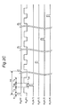
- drive pulses ⁇ T (n, A2) and ⁇ T (n, B2) as well as ⁇ T (n, A4) and ⁇ T (n, B4) turn ON simultaneously, and totally four pixels, i.e. pixel signals of the 1st column and the 3rd column of the 2nd row as well as pixel signals of the 1st column and the 3rd column of the 4th row, are added up and led to the signal line 7 of the j-th column, while totally four pixels, i.e. pixel signals of the 2nd column and the 4th column of the 2nd row as well as pixel signals of the 2nd column and the 4th column of the 4th row, are added up and led to the signal line 11 of the (j+1)th column.
Landscapes
- Engineering & Computer Science (AREA)
- Multimedia (AREA)
- Signal Processing (AREA)
- Chemical & Material Sciences (AREA)
- Inorganic Chemistry (AREA)
- Chemical Kinetics & Catalysis (AREA)
- Solid State Image Pick-Up Elements (AREA)
- Transforming Light Signals Into Electric Signals (AREA)
- Color Television Image Signal Generators (AREA)
Abstract
Description

Since s12 = 2·s1 and n12 = na1,
the signal charges of the photoelectric conversion elements are added up which have an identical color characteristic.
the signal charges of the photoelectric conversion elements are added up which have different color characteristics composing a combination of a specified plurality of colors, respectively.
in each of the photoelectric conversion transfer parts, the transfer transistors are composed of an odd-numbered field transfer transistor and an even-numbered field transfer transistor which respectively transfer signal charge of the photoelectric conversion element,
the switched capacitor amplification part includes an odd-numbered field switched capacitor amplification part whose input side is connected to an output side of the odd-numbered field transfer transistor and an even-numbered field switched capacitor amplification part whose input side is connected to an output side of the even-numbered field transfer transistor,
the control part includes an odd-numbered field control part for controlling the odd-numbered field transfer transistor and the odd-numbered field switched capacitor amplification part as well as an even-numbered field control part for controlling the even-numbered field transfer transistor and the even-numbered field switched capacitor amplification part, and
the odd-numbered field control part and the even-numbered field control part perform interlace reading of a columnar-direction combination of photoelectric conversion elements to be added to the odd-numbered field switched capacitor amplification part side as well as a columnar-direction combination of photoelectric conversion elements to be added to the even-numbered field switched capacitor amplification part side each with a shift of one row in the columnar direction.
Claims (6)
- An amplifying solid-state image pickup device comprising:a plurality of photoelectric conversion transfer parts (10) which are provided for individual pixels (30), respectively, and each of which has a photoelectric conversion element (1) and at least one transfer transistor (2, 2a, 2b) for transferring signal charge of the photoelectric conversion element (1), whereinthe plurality of photoelectric conversion transfer parts (10) are divided into a plurality of photoelectric conversion transfer part groups each composed of at least two of the photoelectric conversion transfer parts (10), respectively;a plurality of switched capacitor amplification parts (20, 20a, 20b) which are provided for the individual photoelectric conversion transfer part groups, respectively, of which input side of each is connected to an output side of each transfer transistor (2, 2a, 2b) of the photoelectric conversion transfer parts (10) and of which output side of each is connected to a signal line; anda control part (25, 25a, 25b) for selecting a plurality of photoelectric conversion transfer parts (10) out of all the photoelectric conversion transfer parts (10) within the photoelectric conversion transfer part group, and controlling the transfer transistors (2, 2a, 2b) and the switched capacitor amplification parts (20, 20a, 20b) so that signal charges of the photoelectric conversion elements (1) of the selected plurality of photoelectric conversion transfer parts (10) are transferred to the input side of the switched capacitor amplification part (20, 20a, 20b) via the transfer transistors (2, 2a, 2b) of the selected plurality of photoelectric conversion transfer parts (10), the plurality of signal charges are added up, and the added-up signal charge is read out by the switched capacitor amplification parts (20, 20a, 20b).
- The amplifying solid-state image pickup device as claimed in Claim 1, wherein
the control part (25) is switchable between an addition operation mode for performing addition of the signal charges and an independent operation mode for independently reading signal charges of the photoelectric conversion elements (1), respectively, without performing the addition of signal charges. - The amplifying solid-state image pickup device as claimed in Claim 1, wherein
the photoelectric conversion element (1) is a buried photodiode. - The amplifying solid-state image pickup device as claimed in Claim 1, wherein
each of the photoelectric conversion elements (1) has any one of a plurality of color characteristics, and
the signal charges of the photoelectric conversion elements (1) are added up which have an identical color characteristic. - The amplifying solid-state image pickup device as claimed in Claim 1, wherein
each of the photoelectric conversion elements (1) has any one of a plurality of color characteristics, and
the signal charges of the photoelectric conversion elements (1) are added up which have different color characteristics composing a combination of a specified plurality of colors, respectively. - The amplifying solid-state image pickup device as claimed in Claim 1, wherein
the photoelectric conversion transfer part groups are arrayed in a matrix shape,
in each of the photoelectric conversion transfer parts (10), the transfer transistors are composed of an odd-numbered field transfer transistor (2a) and an even-numbered field transfer transistor (2b) which respectively transfer signal charge of the photoelectric conversion element (1),
the switched capacitor amplification part includes an odd-numbered field switched capacitor amplification part (20a) whose input side is connected to an output side of the odd-numbered field transfer transistor (2a) and an even-numbered field switched capacitor amplification part (20b) whose input side is connected to an output side of the even-numbered field transfer transistor (2b),
the control part includes an odd-numbered field control part (25a) for controlling the odd-numbered field transfer transistor (2a) and the odd-numbered field switched capacitor amplification part (20a) as well as an even-numbered field control part (25b) for controlling the even-numbered field transfer transistor (2b) and the even-numbered field switched capacitor amplification part (20b), and
the odd-numbered field control part (25a) and the even-numbered field control part (25b) perform interlace reading of a columnar-direction combination of photoelectric conversion elements (1) to be added to the odd-numbered field switched capacitor amplification part (20a) side as well as a columnar-direction combination of photoelectric conversion elements (1) to be added to the even-numbered field switched capacitor amplification part (25b) side each with a shift of one row in the columnar direction.
Applications Claiming Priority (2)
| Application Number | Priority Date | Filing Date | Title |
|---|---|---|---|
| JP2004049482 | 2004-02-25 | ||
| JP2004049482A JP4086798B2 (en) | 2004-02-25 | 2004-02-25 | Amplification type solid-state imaging device |
Publications (2)
| Publication Number | Publication Date |
|---|---|
| EP1569278A2 true EP1569278A2 (en) | 2005-08-31 |
| EP1569278A3 EP1569278A3 (en) | 2007-05-30 |
Family
ID=34747465
Family Applications (1)
| Application Number | Title | Priority Date | Filing Date |
|---|---|---|---|
| EP05251102A Withdrawn EP1569278A3 (en) | 2004-02-25 | 2005-02-24 | Amplifying solid-state image pickup device |
Country Status (5)
| Country | Link |
|---|---|
| US (1) | US6992341B2 (en) |
| EP (1) | EP1569278A3 (en) |
| JP (1) | JP4086798B2 (en) |
| KR (1) | KR100678612B1 (en) |
| CN (1) | CN100338946C (en) |
Cited By (3)
| Publication number | Priority date | Publication date | Assignee | Title |
|---|---|---|---|---|
| CN101534397B (en) * | 2008-03-14 | 2011-06-29 | 佳能株式会社 | Solid state image pickup device |
| EP2351356A4 (en) * | 2008-10-22 | 2014-09-10 | Canon Kk | IMAGE SENSOR AND IMAGE DETECTION APPARATUS |
| EP2890118A4 (en) * | 2012-08-23 | 2016-08-10 | Sony Corp | CURRENT CONVERSION CIRCUIT / VOLTAGE AND IMAGE CAPTURE DEVICE |
Families Citing this family (23)
| Publication number | Priority date | Publication date | Assignee | Title |
|---|---|---|---|---|
| JP4071190B2 (en) * | 2003-12-02 | 2008-04-02 | シャープ株式会社 | Amplification type solid-state imaging device and driving method thereof |
| JP4051034B2 (en) * | 2004-01-28 | 2008-02-20 | シャープ株式会社 | Amplification type solid-state imaging device and driving method thereof |
| KR100871688B1 (en) * | 2004-02-27 | 2008-12-08 | 삼성전자주식회사 | Solid-state imaging device and its driving method |
| JP2005348041A (en) * | 2004-06-02 | 2005-12-15 | Canon Inc | Solid-state imaging device and imaging system |
| JP4828914B2 (en) * | 2005-10-28 | 2011-11-30 | 株式会社東芝 | Solid-state imaging device and driving method thereof |
| JP4902308B2 (en) * | 2006-10-10 | 2012-03-21 | Hoya株式会社 | Image sensor |
| JP4242427B2 (en) * | 2007-02-01 | 2009-03-25 | シャープ株式会社 | Amplification type solid-state imaging device |
| KR100823173B1 (en) | 2007-02-16 | 2008-04-21 | 삼성전자주식회사 | CMOS image sensor |
| JP2008278453A (en) * | 2007-04-03 | 2008-11-13 | Canon Inc | Imaging apparatus and imaging system |
| US20100110245A1 (en) * | 2007-04-18 | 2010-05-06 | Rosnes Corporation | Solid-state imaging device |
| JP2009010862A (en) * | 2007-06-29 | 2009-01-15 | Canon Inc | Driving method of imaging apparatus |
| JP2009021809A (en) * | 2007-07-11 | 2009-01-29 | Canon Inc | Imaging device driving method, imaging device, and imaging system |
| JP5164719B2 (en) * | 2008-07-29 | 2013-03-21 | キヤノン株式会社 | Solid-state imaging device |
| JP5213632B2 (en) * | 2008-10-09 | 2013-06-19 | キヤノン株式会社 | Imaging device |
| JP5267867B2 (en) * | 2009-03-06 | 2013-08-21 | ルネサスエレクトロニクス株式会社 | Imaging device |
| JP5233828B2 (en) | 2009-05-11 | 2013-07-10 | ソニー株式会社 | Solid-state imaging device, driving method of solid-state imaging device, and electronic apparatus |
| JP5146499B2 (en) | 2009-08-08 | 2013-02-20 | 株式会社ニコン | Solid-state image sensor |
| JP5232189B2 (en) * | 2010-03-11 | 2013-07-10 | 株式会社東芝 | Solid-state imaging device |
| JP5764783B2 (en) * | 2012-04-19 | 2015-08-19 | 国立大学法人東北大学 | Solid-state imaging device |
| US9560301B2 (en) * | 2014-05-16 | 2017-01-31 | Taiwan Semiconductor Manufacturing Company, Ltd. | Pixel unit cell having conversion circuit |
| JP6353300B2 (en) * | 2014-07-08 | 2018-07-04 | ソニーセミコンダクタソリューションズ株式会社 | Pixel circuit, semiconductor photodetection device, and radiation counter |
| EP3252445B1 (en) * | 2016-06-01 | 2024-01-03 | ams International AG | Photodetector arrangement having an adjustable output and method for adjusting an output of a photodetector arrangement |
| EP3516691B1 (en) | 2016-10-14 | 2021-09-22 | Huawei Technologies Co., Ltd. | Cmos image sensor |
Family Cites Families (14)
| Publication number | Priority date | Publication date | Assignee | Title |
|---|---|---|---|---|
| JP2977060B2 (en) * | 1992-01-29 | 1999-11-10 | オリンパス光学工業株式会社 | Solid-state imaging device and control method thereof |
| US6903771B2 (en) * | 2000-03-02 | 2005-06-07 | Canon Kabushiki Kaisha | Image pickup apparatus |
| US5739562A (en) * | 1995-08-01 | 1998-04-14 | Lucent Technologies Inc. | Combined photogate and photodiode active pixel image sensor |
| JP3031606B2 (en) * | 1995-08-02 | 2000-04-10 | キヤノン株式会社 | Solid-state imaging device and image imaging device |
| JPH09260627A (en) * | 1996-03-18 | 1997-10-03 | Sharp Corp | Amplification type solid-state imaging device |
| JP2871640B2 (en) * | 1996-12-18 | 1999-03-17 | 日本電気株式会社 | Driving method of solid-state imaging device |
| US6037577A (en) * | 1997-03-11 | 2000-03-14 | Kabushiki Kaisha Toshiba | Amplifying solid-state image pickup device and operating method of the same |
| JP2894341B1 (en) * | 1998-03-12 | 1999-05-24 | 日本電気株式会社 | Driving method of solid-state imaging device |
| US6836291B1 (en) * | 1998-04-30 | 2004-12-28 | Minolta Co., Ltd. | Image pickup device with integral amplification |
| US6956605B1 (en) * | 1998-08-05 | 2005-10-18 | Canon Kabushiki Kaisha | Image pickup apparatus |
| JP3697073B2 (en) * | 1998-08-05 | 2005-09-21 | キヤノン株式会社 | Imaging apparatus and imaging system using the same |
| US6445022B1 (en) * | 1999-04-23 | 2002-09-03 | Micron Technology, Inc. | Increasing pixel conversion gain in CMOS image sensors |
| JP3944829B2 (en) * | 2002-01-17 | 2007-07-18 | ソニー株式会社 | Solid-state imaging device and driving method thereof |
| JP4071190B2 (en) * | 2003-12-02 | 2008-04-02 | シャープ株式会社 | Amplification type solid-state imaging device and driving method thereof |
-
2004
- 2004-02-25 JP JP2004049482A patent/JP4086798B2/en not_active Expired - Fee Related
-
2005
- 2005-02-24 EP EP05251102A patent/EP1569278A3/en not_active Withdrawn
- 2005-02-25 KR KR1020050016037A patent/KR100678612B1/en not_active Expired - Fee Related
- 2005-02-25 CN CNB2005100516764A patent/CN100338946C/en not_active Expired - Fee Related
- 2005-02-25 US US11/067,393 patent/US6992341B2/en not_active Expired - Fee Related
Cited By (5)
| Publication number | Priority date | Publication date | Assignee | Title |
|---|---|---|---|---|
| CN101534397B (en) * | 2008-03-14 | 2011-06-29 | 佳能株式会社 | Solid state image pickup device |
| EP2351356A4 (en) * | 2008-10-22 | 2014-09-10 | Canon Kk | IMAGE SENSOR AND IMAGE DETECTION APPARATUS |
| US9294744B2 (en) | 2008-10-22 | 2016-03-22 | Canon Kabushiki Kaisha | Image sensor and image sensing apparatus with plural vertical output lines |
| EP2890118A4 (en) * | 2012-08-23 | 2016-08-10 | Sony Corp | CURRENT CONVERSION CIRCUIT / VOLTAGE AND IMAGE CAPTURE DEVICE |
| US10009565B2 (en) | 2012-08-23 | 2018-06-26 | Sony Corporation | Current/voltage conversion circuit and imaging apparatus |
Also Published As
| Publication number | Publication date |
|---|---|
| CN1662040A (en) | 2005-08-31 |
| CN100338946C (en) | 2007-09-19 |
| US6992341B2 (en) | 2006-01-31 |
| KR20060042392A (en) | 2006-05-12 |
| JP4086798B2 (en) | 2008-05-14 |
| JP2005244435A (en) | 2005-09-08 |
| EP1569278A3 (en) | 2007-05-30 |
| KR100678612B1 (en) | 2007-02-02 |
| US20050185073A1 (en) | 2005-08-25 |
Similar Documents
| Publication | Publication Date | Title |
|---|---|---|
| US6992341B2 (en) | Amplifying solid-state image pickup device | |
| KR101204571B1 (en) | Solid-state imaging device, method for driving the same and camera | |
| US6784928B1 (en) | Solid state image pickup device and signal reading method thereof | |
| US8023018B2 (en) | Drive method for solid-state imaging device, solid-state imaging device, and imaging apparatus | |
| EP0757497B1 (en) | Photoelectric conversion apparatus for colour images | |
| US9832405B2 (en) | Solid-state imaging device with a plurality of photoelectric converters | |
| KR101104617B1 (en) | Solid state imaging device and imaging device | |
| JP6239975B2 (en) | Solid-state imaging device and imaging system using the same | |
| US7456886B2 (en) | Image pickup apparatus | |
| JP4611296B2 (en) | Charge binning image sensor | |
| US8189081B2 (en) | Solid-state imaging apparatus, driving method thereof, camera, and copier | |
| JP2006253876A (en) | Physical quantity distribution detection device and driving method of physical quantity distribution detection device | |
| JP2011239156A (en) | Solid-state imaging device and camera | |
| US20100245628A1 (en) | Imaging apparatus and imaging system | |
| KR100660862B1 (en) | A color image pickup device for adding and outputting pixel data of the same color and a pixel data reading method thereof | |
| JP3956875B2 (en) | Solid-state imaging device | |
| US8547458B2 (en) | Solid-state image pickup device | |
| US7701498B2 (en) | Solid-state image pickup device, drive method therefor and camera | |
| WO2011007562A1 (en) | Image reader |
Legal Events
| Date | Code | Title | Description |
|---|---|---|---|
| PUAI | Public reference made under article 153(3) epc to a published international application that has entered the european phase |
Free format text: ORIGINAL CODE: 0009012 |
|
| AK | Designated contracting states |
Kind code of ref document: A2 Designated state(s): AT BE BG CH CY CZ DE DK EE ES FI FR GB GR HU IE IS IT LI LT LU MC NL PL PT RO SE SI SK TR |
|
| AX | Request for extension of the european patent |
Extension state: AL BA HR LV MK YU |
|
| PUAL | Search report despatched |
Free format text: ORIGINAL CODE: 0009013 |
|
| AK | Designated contracting states |
Kind code of ref document: A3 Designated state(s): AT BE BG CH CY CZ DE DK EE ES FI FR GB GR HU IE IS IT LI LT LU MC NL PL PT RO SE SI SK TR |
|
| AX | Request for extension of the european patent |
Extension state: AL BA HR LV MK YU |
|
| RIC1 | Information provided on ipc code assigned before grant |
Ipc: H04N 3/15 20060101ALI20070425BHEP Ipc: H01L 27/146 20060101AFI20050628BHEP |
|
| 17P | Request for examination filed |
Effective date: 20070817 |
|
| AKX | Designation fees paid |
Designated state(s): DE FR GB |
|
| 17Q | First examination report despatched |
Effective date: 20100219 |
|
| STAA | Information on the status of an ep patent application or granted ep patent |
Free format text: STATUS: THE APPLICATION IS DEEMED TO BE WITHDRAWN |
|
| 18D | Application deemed to be withdrawn |
Effective date: 20100702 |