EP1569269A1 - Epitaxial growing method and substrate for epitaxial growth - Google Patents
Epitaxial growing method and substrate for epitaxial growth Download PDFInfo
- Publication number
- EP1569269A1 EP1569269A1 EP03723368A EP03723368A EP1569269A1 EP 1569269 A1 EP1569269 A1 EP 1569269A1 EP 03723368 A EP03723368 A EP 03723368A EP 03723368 A EP03723368 A EP 03723368A EP 1569269 A1 EP1569269 A1 EP 1569269A1
- Authority
- EP
- European Patent Office
- Prior art keywords
- substrate
- layer
- growth
- compound semiconductor
- epitaxial growth
- Prior art date
- Legal status (The legal status is an assumption and is not a legal conclusion. Google has not performed a legal analysis and makes no representation as to the accuracy of the status listed.)
- Granted
Links
Images
Classifications
-
- C—CHEMISTRY; METALLURGY
- C30—CRYSTAL GROWTH
- C30B—SINGLE-CRYSTAL GROWTH; UNIDIRECTIONAL SOLIDIFICATION OF EUTECTIC MATERIAL OR UNIDIRECTIONAL DEMIXING OF EUTECTOID MATERIAL; REFINING BY ZONE-MELTING OF MATERIAL; PRODUCTION OF A HOMOGENEOUS POLYCRYSTALLINE MATERIAL WITH DEFINED STRUCTURE; SINGLE CRYSTALS OR HOMOGENEOUS POLYCRYSTALLINE MATERIAL WITH DEFINED STRUCTURE; AFTER-TREATMENT OF SINGLE CRYSTALS OR A HOMOGENEOUS POLYCRYSTALLINE MATERIAL WITH DEFINED STRUCTURE; APPARATUS THEREFOR
- C30B25/00—Single-crystal growth by chemical reaction of reactive gases, e.g. chemical vapour-deposition growth
- C30B25/02—Epitaxial-layer growth
-
- H—ELECTRICITY
- H10—SEMICONDUCTOR DEVICES; ELECTRIC SOLID-STATE DEVICES NOT OTHERWISE PROVIDED FOR
- H10P—GENERIC PROCESSES OR APPARATUS FOR THE MANUFACTURE OR TREATMENT OF DEVICES COVERED BY CLASS H10
- H10P14/00—Formation of materials, e.g. in the shape of layers or pillars
- H10P14/20—Formation of materials, e.g. in the shape of layers or pillars of semiconductor materials
-
- C—CHEMISTRY; METALLURGY
- C30—CRYSTAL GROWTH
- C30B—SINGLE-CRYSTAL GROWTH; UNIDIRECTIONAL SOLIDIFICATION OF EUTECTIC MATERIAL OR UNIDIRECTIONAL DEMIXING OF EUTECTOID MATERIAL; REFINING BY ZONE-MELTING OF MATERIAL; PRODUCTION OF A HOMOGENEOUS POLYCRYSTALLINE MATERIAL WITH DEFINED STRUCTURE; SINGLE CRYSTALS OR HOMOGENEOUS POLYCRYSTALLINE MATERIAL WITH DEFINED STRUCTURE; AFTER-TREATMENT OF SINGLE CRYSTALS OR A HOMOGENEOUS POLYCRYSTALLINE MATERIAL WITH DEFINED STRUCTURE; APPARATUS THEREFOR
- C30B25/00—Single-crystal growth by chemical reaction of reactive gases, e.g. chemical vapour-deposition growth
- C30B25/02—Epitaxial-layer growth
- C30B25/18—Epitaxial-layer growth characterised by the substrate
- C30B25/183—Epitaxial-layer growth characterised by the substrate being provided with a buffer layer, e.g. a lattice matching layer
-
- C—CHEMISTRY; METALLURGY
- C30—CRYSTAL GROWTH
- C30B—SINGLE-CRYSTAL GROWTH; UNIDIRECTIONAL SOLIDIFICATION OF EUTECTIC MATERIAL OR UNIDIRECTIONAL DEMIXING OF EUTECTOID MATERIAL; REFINING BY ZONE-MELTING OF MATERIAL; PRODUCTION OF A HOMOGENEOUS POLYCRYSTALLINE MATERIAL WITH DEFINED STRUCTURE; SINGLE CRYSTALS OR HOMOGENEOUS POLYCRYSTALLINE MATERIAL WITH DEFINED STRUCTURE; AFTER-TREATMENT OF SINGLE CRYSTALS OR A HOMOGENEOUS POLYCRYSTALLINE MATERIAL WITH DEFINED STRUCTURE; APPARATUS THEREFOR
- C30B29/00—Single crystals or homogeneous polycrystalline material with defined structure characterised by the material or by their shape
- C30B29/10—Inorganic compounds or compositions
- C30B29/40—AIIIBV compounds wherein A is B, Al, Ga, In or Tl and B is N, P, As, Sb or Bi
-
- H—ELECTRICITY
- H10—SEMICONDUCTOR DEVICES; ELECTRIC SOLID-STATE DEVICES NOT OTHERWISE PROVIDED FOR
- H10P—GENERIC PROCESSES OR APPARATUS FOR THE MANUFACTURE OR TREATMENT OF DEVICES COVERED BY CLASS H10
- H10P14/00—Formation of materials, e.g. in the shape of layers or pillars
- H10P14/20—Formation of materials, e.g. in the shape of layers or pillars of semiconductor materials
- H10P14/29—Formation of materials, e.g. in the shape of layers or pillars of semiconductor materials characterised by the substrates
- H10P14/2901—Materials
- H10P14/2907—Materials being Group IIIA-VA materials
- H10P14/2909—Phosphides
-
- H—ELECTRICITY
- H10—SEMICONDUCTOR DEVICES; ELECTRIC SOLID-STATE DEVICES NOT OTHERWISE PROVIDED FOR
- H10P—GENERIC PROCESSES OR APPARATUS FOR THE MANUFACTURE OR TREATMENT OF DEVICES COVERED BY CLASS H10
- H10P14/00—Formation of materials, e.g. in the shape of layers or pillars
- H10P14/20—Formation of materials, e.g. in the shape of layers or pillars of semiconductor materials
- H10P14/29—Formation of materials, e.g. in the shape of layers or pillars of semiconductor materials characterised by the substrates
- H10P14/2926—Crystal orientations
-
- H—ELECTRICITY
- H10—SEMICONDUCTOR DEVICES; ELECTRIC SOLID-STATE DEVICES NOT OTHERWISE PROVIDED FOR
- H10P—GENERIC PROCESSES OR APPARATUS FOR THE MANUFACTURE OR TREATMENT OF DEVICES COVERED BY CLASS H10
- H10P14/00—Formation of materials, e.g. in the shape of layers or pillars
- H10P14/20—Formation of materials, e.g. in the shape of layers or pillars of semiconductor materials
- H10P14/32—Formation of materials, e.g. in the shape of layers or pillars of semiconductor materials characterised by intermediate layers between substrates and deposited layers
- H10P14/3202—Materials thereof
- H10P14/3214—Materials thereof being Group IIIA-VA semiconductors
- H10P14/3218—Phosphides
-
- H—ELECTRICITY
- H10—SEMICONDUCTOR DEVICES; ELECTRIC SOLID-STATE DEVICES NOT OTHERWISE PROVIDED FOR
- H10P—GENERIC PROCESSES OR APPARATUS FOR THE MANUFACTURE OR TREATMENT OF DEVICES COVERED BY CLASS H10
- H10P14/00—Formation of materials, e.g. in the shape of layers or pillars
- H10P14/20—Formation of materials, e.g. in the shape of layers or pillars of semiconductor materials
- H10P14/32—Formation of materials, e.g. in the shape of layers or pillars of semiconductor materials characterised by intermediate layers between substrates and deposited layers
- H10P14/3202—Materials thereof
- H10P14/3214—Materials thereof being Group IIIA-VA semiconductors
- H10P14/3221—Arsenides
-
- H—ELECTRICITY
- H10—SEMICONDUCTOR DEVICES; ELECTRIC SOLID-STATE DEVICES NOT OTHERWISE PROVIDED FOR
- H10P—GENERIC PROCESSES OR APPARATUS FOR THE MANUFACTURE OR TREATMENT OF DEVICES COVERED BY CLASS H10
- H10P14/00—Formation of materials, e.g. in the shape of layers or pillars
- H10P14/20—Formation of materials, e.g. in the shape of layers or pillars of semiconductor materials
- H10P14/32—Formation of materials, e.g. in the shape of layers or pillars of semiconductor materials characterised by intermediate layers between substrates and deposited layers
- H10P14/3242—Structure
- H10P14/3244—Layer structure
- H10P14/3248—Layer structure consisting of two layers
-
- H—ELECTRICITY
- H10—SEMICONDUCTOR DEVICES; ELECTRIC SOLID-STATE DEVICES NOT OTHERWISE PROVIDED FOR
- H10P—GENERIC PROCESSES OR APPARATUS FOR THE MANUFACTURE OR TREATMENT OF DEVICES COVERED BY CLASS H10
- H10P14/00—Formation of materials, e.g. in the shape of layers or pillars
- H10P14/20—Formation of materials, e.g. in the shape of layers or pillars of semiconductor materials
- H10P14/34—Deposited materials, e.g. layers
- H10P14/3402—Deposited materials, e.g. layers characterised by the chemical composition
- H10P14/3414—Deposited materials, e.g. layers characterised by the chemical composition being group IIIA-VIA materials
- H10P14/3418—Phosphides
-
- H—ELECTRICITY
- H10—SEMICONDUCTOR DEVICES; ELECTRIC SOLID-STATE DEVICES NOT OTHERWISE PROVIDED FOR
- H10P—GENERIC PROCESSES OR APPARATUS FOR THE MANUFACTURE OR TREATMENT OF DEVICES COVERED BY CLASS H10
- H10P50/00—Etching of wafers, substrates or parts of devices
Definitions
- the present invention relates to an epitaxial growth method or a substrate for epitaxial growth; for forming a compound semiconductor layer on a semiconductor substrate by metal organic chemical vapor deposition, and especially relates to a technique for improving surface morphology of the compound semiconductor.
- a semiconductor wafer has been widely used for a semiconductor element such as a luminous element and light receiving element, in which a III-V group ternary or quaternary compound semiconductor layer such as an InGaAs layer, AlGaAs layer, InAlAs layer, InAlGaAs layer and InGaAsP layer and an InP layer are sequentially grown onto an InP substrate by epitaxial growth.
- the epitaxial layer of this semiconductor wafer is, for example, formed by metal organic chemical vapor deposition (hereinafter referred to as an MOCVD method).
- JP2750331B discloses that plane orientation of a substrate in epitaxial growth is regulated in order to reduce a teardrop-like defect (synonymous with a hillock-like defect) occurring on a surface of a growth film.
- plane orientation of a compound semiconductor single crystal substrate to be used is regulated according to a growth temperature and growth rate in growing the epitaxial layer, so that an occurrence of the teardrop-like defect is effectively reduced.
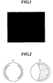
- aberrant surface morphology a surface of an epitaxial growth layer (hereinafter referred to as aberrant surface morphology) (see FIG. 1).
- the present invention is made in order to solve the above problems.
- the object of the invention is to provide an epitaxial growth method and a substrate for growth used for epitaxial growth, in which occurrence of the aberrant surface morphology is effectively prevented in a course of growing a III-V group compound semiconductor layer such as InGaAs layer, AlGaAs layer, AlInAs layer and AlInGaAs layer on a InP substrate.
- the present inventors investigated surface morphology of a semiconductor wafer in which an InGaAs layer had been grown on an InP substrate by the above-described technique of prior art.
- the InGaAs layer was grown to be thinner than 0.5 ⁇ m thick, the aberrant surface morphology as shown in FIG. 1 was not observed at all, and only when the InGaAs layer was grown to be thicker than 0.5 ⁇ m, aberrant surface morphology was observed.
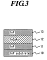
- the aberrant surface morphology may occur along with edges of a substrate as shown in FIG. 2(a), or at approximately a half area of a substrate as shown in FIG. 2(b). It was found that the generation part varied according to substrates to be used. The present inventors presumed that plane orientation generally has slight variation in an entire area of a substrate, which caused the substrates to show various generation status (generation part) of aberrant surface morphology as described above.
- the aberrant surface morphology especially occurred at a part having certain specific plane orientation, for example one inclined 0.03° to 0.04° with respect to (100) surface. That is, occurrence of the above-described aberrant surface morphology was based on an generation mechanism inherently different from that of a hillock-like defect which occurs at dislocation part of a substance, and it only depended on plane orientation of a substrate without any relation to dislocation of a substrate.
- the inventors acquired a knowledge that occurrence of the aberrant surface morphology can be prevented by using a substrate not having certain plane orientation in the entire area of the substrate, when a III-V group compound semiconductor layer such as InGaAs layer is grown to be 0.5 ⁇ m thick or more by epitaxial growth on a substrate for growth such as InP single crystal.
- the present invention is made on the basis of the above knowledge, and is an epitaxial growth method comprising supporting a substrate for growth with a substrate supporter, growing a compound semiconductor layer comprising three or four elements on the semiconductor substrate by metal organic chemical vapor deposition, polishing the substrate so that an angle of gradient direction is 0.00° to 0.03° or 0.04° to 0.24° with respect to (100) in an entire effective area of the substrate, and forming the compound semiconductor layer to be 0.5 ⁇ m thick or more on the substrate by using the substrate for growth. That is, since the aberrant surface morphology occurs in the case that the angle of gradient with respect to (100) surface is 0.03° to 0.04°, a substrate not including a portion having such plane orientation is used.
- the effective area designates a center part of a substrate, eliminating a rolled edge occurring in mirror finishing process located at the most peripheral part thereof (approximately 3mm width from the circumference of the substrate).
- the compound semiconductor layer may be formed on the substrate for growth by the intermediary of a buffer layer. By doing so, the compound semiconductor layer having superior crystal quality can be grown with epitaxial growth.
- III-V group compound semiconductor layer containing at least As on the substrate for growth is also effective in growing a III-V group compound semiconductor layer containing at least As on the substrate for growth.
- the compound semiconductor layer is an InGaAs layer or InAlAs layer.
- the above non-patent literature 1 discloses that a hillock-like defect occurs when an angle of gradient is 0.00° to 0.03°. However, as described above, the hillock-like defect occurs only at a crystal having dislocation. Thus, the occurrence of hillock-like defect can be prevented by using a crystal substrate having sufficiently low dislocation density or no dislocation. Concretely, it is desirable to use a semiconductor crystal substrate having dislocation density of 5000cm -2 or less.
- the substrate for growth which has been previously polished so that an angle of gradient is 0.00° to 0.03° or 0.04° to 0.24° with respect to (100) direction in entire effective area of the substrate may be used.
- an InP single crystal grown in (100) direction was manufactured with liquid encapsulated Czochralski (LEC) method in order to obtain the substrate for growth to which the present invention is to be applied.
- LOC liquid encapsulated Czochralski
- Sulfur, tin and iron were respectively used as a dopant so that a plurality of InP single crystals having different dislocation densities each other were obtained.
- the dislocation densities of the InP single crystals were 500cm -2 or less (sulfur dope), 5000cm -2 (tin dope) and 20000cm -2 (iron dope) respectively.
- Each InP single crystal was formed to be a circular cylinder of 2 inches diameter, and sliced to obtain an InP substrate in which the surface thereof slopes 0.00° to 0.30° with respect to (100) surface.
- an epitaxial layer was formed onto these substrates with metal organic chemical vapor deposition, so that semiconductor wafer of a laminated structure as shown in FIG. 3 was manufactured.
- an InP buffer layer 11 of 0.5 ⁇ m thick was formed onto an InP substrate 10, and an InGaAs layer 12 of 0.3 to 2.5 ⁇ m thick is formed thereon.
- an InP layer 13 of 0.5 ⁇ m thick is formed.
- growth temperature was set to 640°C
- growth pressure is set to 50torr
- total gas flow is set to 601/min.
- growth rate of the InGaAs layer 12 was set to 1.0 ⁇ m/h
- growth rates of the InP layers 11 and 13 were set to 2.0 ⁇ m/h.
- occurrence of the aberrant surface morphology could be prevented by using the substrates having an angle of gradient with respect to (100) surface of 0.00° to 0.03° or 0.04° or more. Further, occurrence of hillock-like defect could be prevented by using the substrates having dislocation density of 5000cm -2 or less, and occurrence of step-like defect could be prevented when an angle of gradient was 0.25° or less with respect to (100) surface.
- an example where an InGaAs layer is grown on an InP substrate with epitaxial growth is explained.
- the present invention can be applied to a case where the III-V group compound semiconductor layer comprising 3 or 4 elements including at least As (for example, an AlGaAs layer, AlInAs layer and AlInGaAs layer) is grown to be more than 0.5 ⁇ m thick on the InP substrate with epitaxial growth, similarly with the above case.
- an InP single crystal grown in (100) direction in the entire effective area with LEC method is processed so as to obtain a desired substrate for growth.
- a substrate for growth which has been previously polished so that an angle of gradient is 0.00° to 0.03° or 0.04° to 0.24° with respect to (100) direction also can be used.
- an epitaxial growth method comprises supporting a substrate for growth with a substrate supporter, growing a compound semiconductor layer comprising 3 or 4 elements on the semiconductor substrate by metal organic chemical vapor deposition, polishing the substrate so that an angle of gradient with respect to (100) direction is 0.00° to 0.03° or 0.04° to 0.24° in an entire effective area of the substrate, and forming the compound semiconductor layer to be 0.5 ⁇ m thick or more on the substrate by using the substrate for growth.
- the present invention can be applied not only to a case where a III-V group compound semiconductor layer is grown on an InP substrate, but also to a case where the compound semiconductor layer is grown on a crystal substrate with epitaxial growth using the crystal substrate in which a difference of lattice constant is small between the substrate and the compound semiconductor layer to be grown.
Landscapes
- Chemical & Material Sciences (AREA)
- Engineering & Computer Science (AREA)
- Crystallography & Structural Chemistry (AREA)
- Materials Engineering (AREA)
- Metallurgy (AREA)
- Organic Chemistry (AREA)
- Chemical Kinetics & Catalysis (AREA)
- General Chemical & Material Sciences (AREA)
- Inorganic Chemistry (AREA)
- Crystals, And After-Treatments Of Crystals (AREA)
- Semiconductor Lasers (AREA)
Abstract
Description

Claims (9)
- An epitaxial growth method comprising: supporting a substrate for growth with a substrate supporter, forming a compound semiconductor layer comprising 3 or 4 elements on the substrate for growth by metal organic chemical vapor deposition, polishing the substrate so that an angle of gradient is 0.00° to 0.03° or 0.04° to 0.24° with respect to (100) direction in an entire effective area of the substrate, and forming the compound semiconductor layer to be 0.5µm thick or more on the substrate by using the substrate for growth.
- The epitaxial growth method as claimed in claim 1, further comprising: forming a buffer layer on the substrate for growth, and forming the compound semiconductor layer on the buffer layer.
- The epitaxial growth method as claimed in claim 1 or 2, wherein the compound semiconductor layer is a III-V group compound semiconductor layer containing at least As.
- The epitaxial growth method as claimed in claim 3, wherein the compound semiconductor layer is an InGaAs layer or an InAlAs layer.
- The epitaxial growth method as claimed in claim 3 or 4, wherein the substrate for growth is a semiconductor crystal substrate having dislocation density of 5000cm-2 or less.
- The epitaxial growth method as claimed in claim 5, wherein the substrate for growth is an InP substrate.
- A substrate for epitaxial growth used for an epitaxial growth method in which a compound semiconductor layer comprising 3 or 4 elements is formed on the substrate for growth by metal organic chemical vapor deposition, wherein an angle of gradient is 0.00° to 0.03° or 0.04° to 0.24° with respect to (100) direction in an entire effective area of the substrate.
- The substrate for epitaxial growth as claimed in claim 7, wherein the substrate is a semiconductor crystal substrate having dislocation density of 5000cm-2 or less.
- The substrate for epitaxial growth as claimed in claim 7 or 8, wherein the substrate is an InP substrate.
Applications Claiming Priority (3)
| Application Number | Priority Date | Filing Date | Title |
|---|---|---|---|
| JP2002350704 | 2002-12-03 | ||
| JP2002350704 | 2002-12-03 | ||
| PCT/JP2003/005987 WO2004051725A1 (en) | 2002-12-03 | 2003-05-14 | Epitaxial growing method and substrate for epitaxial growth |
Publications (3)
| Publication Number | Publication Date |
|---|---|
| EP1569269A1 true EP1569269A1 (en) | 2005-08-31 |
| EP1569269A4 EP1569269A4 (en) | 2007-10-24 |
| EP1569269B1 EP1569269B1 (en) | 2010-12-08 |
Family
ID=32463114
Family Applications (1)
| Application Number | Title | Priority Date | Filing Date |
|---|---|---|---|
| EP03723368A Expired - Lifetime EP1569269B1 (en) | 2002-12-03 | 2003-05-14 | Epitaxial growing method and use of substrate for epitaxial growth |
Country Status (8)
| Country | Link |
|---|---|
| US (1) | US7338902B2 (en) |
| EP (1) | EP1569269B1 (en) |
| JP (1) | JP4657724B2 (en) |
| KR (1) | KR100952650B1 (en) |
| CN (1) | CN100401482C (en) |
| CA (1) | CA2505631C (en) |
| DE (1) | DE60335287D1 (en) |
| WO (1) | WO2004051725A1 (en) |
Families Citing this family (2)
| Publication number | Priority date | Publication date | Assignee | Title |
|---|---|---|---|---|
| TWI402896B (en) * | 2006-02-02 | 2013-07-21 | Nippon Mining Co | Substrate semiconductor growth substrate and epitaxial growth method |
| FR2921200B1 (en) * | 2007-09-18 | 2009-12-18 | Centre Nat Rech Scient | EPITAXIC MONOLITHIC SEMICONDUCTOR HETEROSTRUCTURES AND PROCESS FOR THEIR MANUFACTURE |
Family Cites Families (4)
| Publication number | Priority date | Publication date | Assignee | Title |
|---|---|---|---|---|
| JPH0692278B2 (en) | 1989-03-09 | 1994-11-16 | 株式会社ジャパンエナジー | Epitaxial growth method |
| JP2750331B2 (en) | 1992-04-23 | 1998-05-13 | 株式会社ジャパンエナジー | Substrate for epitaxial growth and epitaxial growth method |
| JP3129112B2 (en) * | 1994-09-08 | 2001-01-29 | 住友電気工業株式会社 | Compound semiconductor epitaxial growth method and InP substrate therefor |
| JPH08330236A (en) | 1995-05-30 | 1996-12-13 | Furukawa Electric Co Ltd:The | Metal organic chemical vapor deposition |
-
2003
- 2003-05-14 KR KR1020057009830A patent/KR100952650B1/en not_active Expired - Lifetime
- 2003-05-14 US US10/534,695 patent/US7338902B2/en not_active Expired - Lifetime
- 2003-05-14 EP EP03723368A patent/EP1569269B1/en not_active Expired - Lifetime
- 2003-05-14 DE DE60335287T patent/DE60335287D1/en not_active Expired - Lifetime
- 2003-05-14 CA CA2505631A patent/CA2505631C/en not_active Expired - Lifetime
- 2003-05-14 CN CNB038255286A patent/CN100401482C/en not_active Expired - Lifetime
- 2003-05-14 JP JP2004556817A patent/JP4657724B2/en not_active Expired - Lifetime
- 2003-05-14 WO PCT/JP2003/005987 patent/WO2004051725A1/en not_active Ceased
Also Published As
| Publication number | Publication date |
|---|---|
| JP4657724B2 (en) | 2011-03-23 |
| US20060012010A1 (en) | 2006-01-19 |
| DE60335287D1 (en) | 2011-01-20 |
| EP1569269A4 (en) | 2007-10-24 |
| JPWO2004051725A1 (en) | 2006-04-06 |
| KR100952650B1 (en) | 2010-04-13 |
| CN100401482C (en) | 2008-07-09 |
| WO2004051725A1 (en) | 2004-06-17 |
| EP1569269B1 (en) | 2010-12-08 |
| CN1708836A (en) | 2005-12-14 |
| KR20050085234A (en) | 2005-08-29 |
| US7338902B2 (en) | 2008-03-04 |
| CA2505631C (en) | 2012-02-28 |
| CA2505631A1 (en) | 2004-06-17 |
Similar Documents
| Publication | Publication Date | Title |
|---|---|---|
| EP1684973B1 (en) | Vicinal gallium nitride substrate for high quality homoepitaxy | |
| KR100810554B1 (en) | How to improve epitaxy quality (surface texture and defect density) on freestanding (aluminum, indium, gallium) nitride substrates for optoelectronic and electronic devices | |
| US8212259B2 (en) | III-V nitride homoepitaxial material of improved quality formed on free-standing (Al,In,Ga)N substrates | |
| JP2003321298A (en) | SiC single crystal and its manufacturing method, SiC wafer with epitaxial film and its manufacturing method, and SiC electronic device | |
| TWI254362B (en) | Epitaxial growth method | |
| EP1569269B1 (en) | Epitaxial growing method and use of substrate for epitaxial growth | |
| EP1988194B1 (en) | Substrate for growing of compound semiconductor and method of epitaxial growth | |
| CA2556824A1 (en) | Vapor phase growth method | |
| EP1791171B1 (en) | Epitaxial crystal growing method | |
| US7393412B2 (en) | Method for manufacturing compound semiconductor epitaxial substrate | |
| JP2007019048A (en) | Epitaxial growth method and substrate for epitaxial growth |
Legal Events
| Date | Code | Title | Description |
|---|---|---|---|
| PUAI | Public reference made under article 153(3) epc to a published international application that has entered the european phase |
Free format text: ORIGINAL CODE: 0009012 |
|
| 17P | Request for examination filed |
Effective date: 20050622 |
|
| AK | Designated contracting states |
Kind code of ref document: A1 Designated state(s): AT BE BG CH CY CZ DE DK EE ES FI FR GB GR HU IE IT LI LU MC NL PT RO SE SI SK TR |
|
| RBV | Designated contracting states (corrected) |
Designated state(s): DE FR GB |
|
| RAP1 | Party data changed (applicant data changed or rights of an application transferred) |
Owner name: NIPPON MINING & METALS CO., LTD. |
|
| A4 | Supplementary search report drawn up and despatched |
Effective date: 20070920 |
|
| 17Q | First examination report despatched |
Effective date: 20080219 |
|
| RTI1 | Title (correction) |
Free format text: EPITAXIAL GROWING METHOD AND USE OF SUBSTRATE FOR EPITAXIAL GROWTH |
|
| GRAP | Despatch of communication of intention to grant a patent |
Free format text: ORIGINAL CODE: EPIDOSNIGR1 |
|
| GRAS | Grant fee paid |
Free format text: ORIGINAL CODE: EPIDOSNIGR3 |
|
| GRAA | (expected) grant |
Free format text: ORIGINAL CODE: 0009210 |
|
| AK | Designated contracting states |
Kind code of ref document: B1 Designated state(s): DE FR GB |
|
| REG | Reference to a national code |
Ref country code: GB Ref legal event code: FG4D |
|
| REF | Corresponds to: |
Ref document number: 60335287 Country of ref document: DE Date of ref document: 20110120 Kind code of ref document: P |
|
| PLBE | No opposition filed within time limit |
Free format text: ORIGINAL CODE: 0009261 |
|
| STAA | Information on the status of an ep patent application or granted ep patent |
Free format text: STATUS: NO OPPOSITION FILED WITHIN TIME LIMIT |
|
| 26N | No opposition filed |
Effective date: 20110909 |
|
| REG | Reference to a national code |
Ref country code: DE Ref legal event code: R097 Ref document number: 60335287 Country of ref document: DE Effective date: 20110909 |
|
| REG | Reference to a national code |
Ref country code: GB Ref legal event code: 732E Free format text: REGISTERED BETWEEN 20130801 AND 20130807 |
|
| REG | Reference to a national code |
Ref country code: DE Ref legal event code: R081 Ref document number: 60335287 Country of ref document: DE Owner name: JX NIPPON MINING & METALS CORP., JP Free format text: FORMER OWNER: NIPPON MINING & METALS CO., LTD., TOKIO/TOKYO, JP Effective date: 20130715 |
|
| REG | Reference to a national code |
Ref country code: FR Ref legal event code: CD Owner name: JX NIPPON MINING & METALS CORPORATION, JP Effective date: 20130819 Ref country code: FR Ref legal event code: CA Effective date: 20130819 Ref country code: FR Ref legal event code: TP Owner name: JX NIPPON MINING & METALS CORPORATION, JP Effective date: 20130819 |
|
| REG | Reference to a national code |
Ref country code: FR Ref legal event code: PLFP Year of fee payment: 14 |
|
| REG | Reference to a national code |
Ref country code: FR Ref legal event code: PLFP Year of fee payment: 15 |
|
| REG | Reference to a national code |
Ref country code: FR Ref legal event code: CA Effective date: 20171006 |
|
| REG | Reference to a national code |
Ref country code: FR Ref legal event code: PLFP Year of fee payment: 16 |
|
| PGFP | Annual fee paid to national office [announced via postgrant information from national office to epo] |
Ref country code: GB Payment date: 20220519 Year of fee payment: 20 Ref country code: FR Payment date: 20220523 Year of fee payment: 20 Ref country code: DE Payment date: 20220519 Year of fee payment: 20 |
|
| REG | Reference to a national code |
Ref country code: DE Ref legal event code: R071 Ref document number: 60335287 Country of ref document: DE |
|
| REG | Reference to a national code |
Ref country code: GB Ref legal event code: PE20 Expiry date: 20230513 |
|
| PG25 | Lapsed in a contracting state [announced via postgrant information from national office to epo] |
Ref country code: GB Free format text: LAPSE BECAUSE OF EXPIRATION OF PROTECTION Effective date: 20230513 |