EP1569074A1 - Noise-resistant touch-pad using capacitance - Google Patents
Noise-resistant touch-pad using capacitance Download PDFInfo
- Publication number
- EP1569074A1 EP1569074A1 EP04002350A EP04002350A EP1569074A1 EP 1569074 A1 EP1569074 A1 EP 1569074A1 EP 04002350 A EP04002350 A EP 04002350A EP 04002350 A EP04002350 A EP 04002350A EP 1569074 A1 EP1569074 A1 EP 1569074A1
- Authority
- EP
- European Patent Office
- Prior art keywords
- terminal
- film
- positioning device
- coordinate
- contact point
- Prior art date
- Legal status (The legal status is an assumption and is not a legal conclusion. Google has not performed a legal analysis and makes no representation as to the accuracy of the status listed.)
- Granted
Links
Images



Classifications
-
- G—PHYSICS
- G06—COMPUTING OR CALCULATING; COUNTING
- G06F—ELECTRIC DIGITAL DATA PROCESSING
- G06F3/00—Input arrangements for transferring data to be processed into a form capable of being handled by the computer; Output arrangements for transferring data from processing unit to output unit, e.g. interface arrangements
- G06F3/01—Input arrangements or combined input and output arrangements for interaction between user and computer
- G06F3/03—Arrangements for converting the position or the displacement of a member into a coded form
- G06F3/041—Digitisers, e.g. for touch screens or touch pads, characterised by the transducing means
- G06F3/045—Digitisers, e.g. for touch screens or touch pads, characterised by the transducing means using resistive elements, e.g. a single continuous surface or two parallel surfaces put in contact
Definitions
- the invention relates to a film positioning device, and more particularly to a film positioning device having a quick response speed.
- a cursor positioning device such as a mouse or a film positioning device, is widely used in the man-machine interface to facilitate the communication between the user and the electrical device.
- the film positioning device includes two resistive films or two capacitive films for detecting coordinates of a point contacted by the user.
- FIG. 1 shows a circuit diagram of a resistive film positioning device 100, which includes a film 110.
- the film 110 includes an X film and a Y film.
- the X film and the Y film are plane resistors and do not contact each other in a natural state.
- the resistance on the X film varies with the variation of the X coordinate but does not depend on the variation of the Y coordinate.
- the resistance on the Y film varies with the variation of the Y coordinate but does not depend on the variation of the X coordinate.
- the film positioning device further includes transistors QX0, QX1, QY0, QY1 and capacitors Cxp, Cxm, Cyp and Cym for detecting a point contacted by a user and isolating the noises, wherein the transistors QX0, QX1, QY0 and QY1 are controlled by signals X0, X1, Y0 and Y1, respectively.
- the X film is electrically connected to the Y film at a contact point, and the resistor of the contact point is R_touch.
- the resistor above the contact point is R_up
- the resistor below the contact point is R_down.
- the resistor at the right-hand side of the contact point is R_right
- the resistor at the left-hand side of the contact point is R_left.
- the film positioning device 100 may obtain the X coordinate of the contact point according to the ratio of the resistor R_up to the resistor R_down, and the Y coordinate of the contact point according to the ratio of the resistor R_right to the resistor R_left.
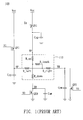
- FIG. 2A shows an equivalent circuit diagram of the film positioning device when the X coordinate of a contact point is detected.
- the transistors QY0 and QY1 are turned on, and then the current I1 flows to the ground via QY1, R_left, R_right and QY0.
- the X coordinate of the contact point may be obtained by detecting the voltage at the XP point.
- the X coordinate of the contact point also may be obtained by detecting the voltage at the XM point.
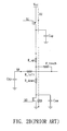
- FIG. 2B shows an equivalent circuit diagram of the film positioning device when the Y coordinate of the contact point is detected.
- the transistors QXO and QX1 are turned on, and then the current 12 flows to the ground via QX1, R_up, R_down and QX0.
- the Y coordinate of the contact point may be obtained by detecting the voltage at the YP point.
- the Y coordinate of the contact point also may be obtained by detecting the voltage at the YM point.
- the capacitors Cxp, Cxm, Cyp and Cym are used to isolate noises and ensure the precision of the coordinates. As the capacitances of the capacitors get larger, the capability of isolating noises gets greater, but the response speed of the positioning device gets slower.
- the capacitor Cyp is charged to about the level of the power source Vcc.
- the transistors QY1 and QY2 are turned off, so the capacitor Cyp has to be discharged through the impedances of R_left, R_touch, Cxp, and the like.
- the force applied from the user to the film positioning device is too small and thus makes the impedance of R_touch very large, thereby lengthening the discharge time of the capacitor Cyp. If the discharge time of the capacitor Cyp is lengthened, the waiting time for the next coordinate to be detected is also lengthened, thereby causing the problem of the insufficiently quick response speed of the positioning device.
- the capacitor Cxp is charged to about the level of the power source Vcc. If the resistor R_touch is too large, the problem of insufficiently quick response speed of the positioning device owing to the lengthened discharge time will be caused.
- the response speed of the positioning device may be increased when the capacitances of the capacitors Cxp, Cxm, Cyp and Cym are reduced, the capability for isolating the noises and thus the positioning precision will be deteriorated. It is problematic if the capacitances are enlarged because the response speed of the positioning device will become too slow.
- the invention achieves the above-identified object by providing a film positioning device for detecting a position of a contact point.
- the film positioning device includes an X film having a first X terminal and a second X terminal, a Y film having a first Y terminal and a second Y terminal, a first Y switch coupled between the first Y terminal and a ground, a second Y switch coupled between the second Y terminal and the power source, a first X switch coupled between the first X terminal and the ground, a second X switch coupled between the second X terminal and the power source, a first X capacitor coupled between the first X terminal and the second X terminal, and a second Y capacitor coupled between the first Y terminal and the second Y terminal.
- FIG. 1 shows a circuit diagram of a resistive film positioning device.
- FIG. 2A shows an equivalent circuit diagram of the film positioning device when the X coordinate of a contact point is detected.
- FIG. 2B shows an equivalent circuit diagram of the film positioning device when the Y coordinate of the contact point is detected.
- FIG. 3 shows a circuit diagram of a film positioning device according to a preferred embodiment of the invention.
- FIG. 4A shows an equivalent circuit diagram of the film positioning device when the X coordinate of the contact point is detected.
- FIG. 4B shows an equivalent circuit diagram of the film positioning device when the Y coordinate of the contact point is detected.
- FIG. 3 shows a circuit diagram of a film positioning device according to a preferred embodiment of the invention.
- the film positioning device 300 includes a film 310, which includes an X film and a Y film.
- the X film and Y film are plane resistors and do not contact each other in a natural state.
- the resistance on the X film varies with the variation of the X coordinate but does not depend on the variation of the Y coordinate.
- the resistance on the Y film varies with the variation of the Y coordinate but does not depend on the variation of the X coordinate.
- the film positioning device further includes transistors QX0', QX1', QY0' and QY1' and capacitors Cx and Cy for detecting a point contacted by a user and isolating the noises, wherein the transistors QX0', QX1', QY0' and QY1' are controlled by signals X0', X1', Y0' a Y1', respectively.
- the X film is electrically connected to the Y film at a contact point, and the resistor of the contact point is R_touch'.
- the resistor above the contact point is R_up'
- the resistor below the contact point is R_down'
- the resistor at the right-hand side of the contact point is R_right'
- the resistor at the left-hand side of the contact point is R_left'.
- the film positioning device 300 may obtain the X coordinate of the contact point according to the ratio of the resistor R_up' to the resistor R_down', and the Y coordinate of the contact point according to the ratio of the resistor R_right' to the resistor R_left'.
- FIG. 4A shows an equivalent circuit diagram of the film positioning device when the X coordinate of the contact point is detected.
- the transistors QY0' and QY1' are turned on, and then the current I1' flows to the ground via QY1', R_left', R_right' and QY0'.
- the X coordinate of the contact point may be obtained by detecting the voltage at the XP' point.
- the X coordinate of the contact point also may be obtained by detecting the voltage at the XM' point.
- FIG. 4B shows an equivalent circuit diagram of the film positioning device when the Y coordinate of the contact point is detected.
- the transistors QX0' and QX1' are turned on, and then the current 12' flows to the ground via QX1', R_up', R_down' and QX0'.
- the Y coordinate of the contact point may be obtained by detecting the voltage at the YP' point.
- the Y coordinate of the contact point also may be obtained by detecting the voltage at the YM' point.
- a liquid crystal display which has high-frequency signals such as pixel clock signals, horizontal synchronization signals, vertical synchronization signals, and the like so as to maintain an update frequency of, for example, 30 frames per second, is located under the touch panel. The high-frequency signals tend to be coupled to the film positioning device to cause errors in the detected coordinates.
- the invention utilizes newly added capacitors Cx and Cy to isolate the noises, and thus to ensure the precision of the coordinates, shorten the discharge time of these capacitors, and increase the response speed of the positioning device 300.
- the capacitor Cy is charged to about the level of the power source Vcc.
- the transistors QY1' and QY2' are turned off, so the capacitor Cy may be discharged through the impedances of R_left' and R_right' without being discharged through the R_touch' as performed in the prior art method.
- the capacitor Cx is charged to about the level of the power source Vcc.
- the transistors QX1' and QX2' are turned off, so the capacitor Cx may be discharged through R_up' and R_down' without being discharged through R_touch' as performed in the prior art method.
- the embodiment may further include capacitors Cxp', Cxm', Cyp' and Cym' with smaller capacitances to make the effect against noises better without influencing the response speed of the positioning device.
- the disclosed film positioning device changes the coupling manner of the capacitors against the noises and makes its discharge time free from being restricted by the magnitude of the impedance of R_touch', so the positioning speed may be increased and good ability against noises may be obtained.
Landscapes
- Engineering & Computer Science (AREA)
- General Engineering & Computer Science (AREA)
- Theoretical Computer Science (AREA)
- Human Computer Interaction (AREA)
- Physics & Mathematics (AREA)
- General Physics & Mathematics (AREA)
- Position Input By Displaying (AREA)
- Measurement Of Length, Angles, Or The Like Using Electric Or Magnetic Means (AREA)
- Push-Button Switches (AREA)
- Electronic Switches (AREA)
Abstract
Description
Claims (4)
- A film positioning device for detecting a position of a contact point, the device comprising:wherein when the film positioning device detects an X coordinate of the contact point, the first Y switch and the second Y switch are turned on, and then the X coordinate is obtained according to a voltage at the first X terminal or the second X terminal;an X film having a first X terminal and a second X terminal;a Y film having a first Y terminal and a second Y terminal;a first Y switch coupled between the first Y terminal and a ground;a second Y switch coupled between the second Y terminal and a power source;a first X switch coupled between the first X terminal and the ground;a second X switch coupled between the second X terminal and the power source;a first X capacitor coupled between the first X terminal and the second X terminal; anda second Y capacitor coupled between the first Y terminal and the second Y terminal;
wherein when the film positioning device detects a Y coordinate of the contact point, the first X switch and the second X switch are turned on, and then the Y coordinate is obtained according to a voltage at the first Y terminal or the second Y terminal. - The film positioning device according to claim 1, wherein the X film and the Y film are plane resistors.
- The film positioning device according to claim 1, wherein the first Y switch, the second Y switch, the first X switch and the second X switch are transistors.
- The film positioning device according to claim 1, further comprising:a first capacitor coupled to the first X terminal;a second capacitor coupled to the second X terminal;a third capacitor coupled to the first Y terminal; anda fourth capacitor coupled to the second Y terminal.
Priority Applications (3)
| Application Number | Priority Date | Filing Date | Title |
|---|---|---|---|
| EP04002350A EP1569074B1 (en) | 2004-02-03 | 2004-02-03 | Noise-resistant touch-pad using capacitance |
| AT04002350T ATE405880T1 (en) | 2004-02-03 | 2004-02-03 | INTERFERENCE RESISTANT TOUCH SENSITIVE SURFACE USING CAPACITANCE |
| DE602004015927T DE602004015927D1 (en) | 2004-02-03 | 2004-02-03 | Fault-resistant touch-sensitive area using capacitance |
Applications Claiming Priority (1)
| Application Number | Priority Date | Filing Date | Title |
|---|---|---|---|
| EP04002350A EP1569074B1 (en) | 2004-02-03 | 2004-02-03 | Noise-resistant touch-pad using capacitance |
Publications (2)
| Publication Number | Publication Date |
|---|---|
| EP1569074A1 true EP1569074A1 (en) | 2005-08-31 |
| EP1569074B1 EP1569074B1 (en) | 2008-08-20 |
Family
ID=34745848
Family Applications (1)
| Application Number | Title | Priority Date | Filing Date |
|---|---|---|---|
| EP04002350A Expired - Lifetime EP1569074B1 (en) | 2004-02-03 | 2004-02-03 | Noise-resistant touch-pad using capacitance |
Country Status (3)
| Country | Link |
|---|---|
| EP (1) | EP1569074B1 (en) |
| AT (1) | ATE405880T1 (en) |
| DE (1) | DE602004015927D1 (en) |
Cited By (2)
| Publication number | Priority date | Publication date | Assignee | Title |
|---|---|---|---|---|
| WO2006003249A3 (en) * | 2004-07-07 | 2006-04-13 | Emfit Oy | Electrical coupling of an electromechanical control unit |
| JP2015212659A (en) * | 2014-05-02 | 2015-11-26 | 株式会社半導体エネルギー研究所 | Detection device, input device, input / output device, and driving method of detection device |
Citations (3)
| Publication number | Priority date | Publication date | Assignee | Title |
|---|---|---|---|---|
| GB1447525A (en) * | 1972-10-13 | 1976-08-25 | Asahi Optical Co Ltd | Camera shutter control circuit |
| EP0309946A2 (en) * | 1987-09-28 | 1989-04-05 | Oki Electric Industry Company, Limited | Pressure-sentitive input apparatus |
| US20030071797A1 (en) * | 2001-10-12 | 2003-04-17 | Wei-Chih Chang | Method for detecting touch-point coordinate for used in a resistive touch panel |
-
2004
- 2004-02-03 EP EP04002350A patent/EP1569074B1/en not_active Expired - Lifetime
- 2004-02-03 AT AT04002350T patent/ATE405880T1/en not_active IP Right Cessation
- 2004-02-03 DE DE602004015927T patent/DE602004015927D1/en not_active Expired - Lifetime
Patent Citations (3)
| Publication number | Priority date | Publication date | Assignee | Title |
|---|---|---|---|---|
| GB1447525A (en) * | 1972-10-13 | 1976-08-25 | Asahi Optical Co Ltd | Camera shutter control circuit |
| EP0309946A2 (en) * | 1987-09-28 | 1989-04-05 | Oki Electric Industry Company, Limited | Pressure-sentitive input apparatus |
| US20030071797A1 (en) * | 2001-10-12 | 2003-04-17 | Wei-Chih Chang | Method for detecting touch-point coordinate for used in a resistive touch panel |
Cited By (2)
| Publication number | Priority date | Publication date | Assignee | Title |
|---|---|---|---|---|
| WO2006003249A3 (en) * | 2004-07-07 | 2006-04-13 | Emfit Oy | Electrical coupling of an electromechanical control unit |
| JP2015212659A (en) * | 2014-05-02 | 2015-11-26 | 株式会社半導体エネルギー研究所 | Detection device, input device, input / output device, and driving method of detection device |
Also Published As
| Publication number | Publication date |
|---|---|
| ATE405880T1 (en) | 2008-09-15 |
| EP1569074B1 (en) | 2008-08-20 |
| DE602004015927D1 (en) | 2008-10-02 |
Similar Documents
| Publication | Publication Date | Title |
|---|---|---|
| US10990230B2 (en) | Circuit, touch chip, and electronic device for capacitance detection | |
| KR101561351B1 (en) | Touch detection device, display device with touch detection function, and electronic apparatus | |
| US9563310B2 (en) | Touch sensing device and method for driving the same | |
| US8618818B2 (en) | Electrostatic capacity type touch sensor | |
| US8115746B2 (en) | Display panel with multi-touch function | |
| US9524054B2 (en) | Integrator and touch sensing system using the same | |
| US8963858B2 (en) | Use of resistive touch screen as a proximity sensor | |
| CN107870692B (en) | Touch driving circuit, touch display device and method of driving touch display device | |
| US10540041B2 (en) | Touch processor, touch display driver integrated circuit chip including touch processor, and method of operating touch processor | |
| US10338439B2 (en) | Touch detection using common electrodes of display device | |
| US9891724B2 (en) | Circuit and stylus for capacitive touchscreen | |
| US11460953B2 (en) | Noise suppression circuit | |
| US20030071797A1 (en) | Method for detecting touch-point coordinate for used in a resistive touch panel | |
| US7301525B2 (en) | Coordinate positioning device and method thereof | |
| TW201619791A (en) | Test apparatus for touch panel and test method thereof | |
| WO2020237503A1 (en) | Capacitance detection circuit, capacitance detection method, touch chip and electronic device | |
| US20100309161A1 (en) | Image display system and method for controlling a touch panel thereof | |
| EP1569074B1 (en) | Noise-resistant touch-pad using capacitance | |
| US20210303097A1 (en) | Capacitance detection circuit and input device | |
| US20140184522A1 (en) | Touch-sensitive display panel | |
| CN106445220B (en) | Touch detection method and capacitive sensing device | |
| EP1630652A1 (en) | Coordinate positioning device with anti-noise method | |
| US20050074095A1 (en) | Film positioning device | |
| US10001892B2 (en) | Self-capacitive touch and force sensing apparatus and self-capacitive touch and force sensing method | |
| JP4285606B2 (en) | Optical amplification mechanism provided in an optical integrated circuit and an amplification device integrated with the mechanism |
Legal Events
| Date | Code | Title | Description |
|---|---|---|---|
| PUAI | Public reference made under article 153(3) epc to a published international application that has entered the european phase |
Free format text: ORIGINAL CODE: 0009012 |
|
| 17P | Request for examination filed |
Effective date: 20050415 |
|
| AK | Designated contracting states |
Kind code of ref document: A1 Designated state(s): AT BE BG CH CY CZ DE DK EE ES FI FR GB GR HU IE IT LI LU MC NL PT RO SE SI SK TR |
|
| AX | Request for extension of the european patent |
Extension state: AL LT LV MK |
|
| AKX | Designation fees paid |
Designated state(s): AT BE BG CH CY CZ DE DK EE ES FI FR GB GR HU IE IT LI LU MC NL PT RO SE SI SK TR |
|
| 17Q | First examination report despatched |
Effective date: 20061206 |
|
| GRAP | Despatch of communication of intention to grant a patent |
Free format text: ORIGINAL CODE: EPIDOSNIGR1 |
|
| RIC1 | Information provided on ipc code assigned before grant |
Ipc: G06F 3/045 20060101AFI20080129BHEP |
|
| GRAS | Grant fee paid |
Free format text: ORIGINAL CODE: EPIDOSNIGR3 |
|
| GRAA | (expected) grant |
Free format text: ORIGINAL CODE: 0009210 |
|
| AK | Designated contracting states |
Kind code of ref document: B1 Designated state(s): AT BE BG CH CY CZ DE DK EE ES FI FR GB GR HU IE IT LI LU MC NL PT RO SE SI SK TR |
|
| REG | Reference to a national code |
Ref country code: GB Ref legal event code: FG4D |
|
| REG | Reference to a national code |
Ref country code: CH Ref legal event code: EP |
|
| REG | Reference to a national code |
Ref country code: IE Ref legal event code: FG4D |
|
| REF | Corresponds to: |
Ref document number: 602004015927 Country of ref document: DE Date of ref document: 20081002 Kind code of ref document: P |
|
| RAP2 | Party data changed (patent owner data changed or rights of a patent transferred) |
Owner name: HTC CORPORATION |
|
| PG25 | Lapsed in a contracting state [announced via postgrant information from national office to epo] |
Ref country code: NL Free format text: LAPSE BECAUSE OF FAILURE TO SUBMIT A TRANSLATION OF THE DESCRIPTION OR TO PAY THE FEE WITHIN THE PRESCRIBED TIME-LIMIT Effective date: 20080820 Ref country code: ES Free format text: LAPSE BECAUSE OF FAILURE TO SUBMIT A TRANSLATION OF THE DESCRIPTION OR TO PAY THE FEE WITHIN THE PRESCRIBED TIME-LIMIT Effective date: 20081201 |
|
| PG25 | Lapsed in a contracting state [announced via postgrant information from national office to epo] |
Ref country code: FI Free format text: LAPSE BECAUSE OF FAILURE TO SUBMIT A TRANSLATION OF THE DESCRIPTION OR TO PAY THE FEE WITHIN THE PRESCRIBED TIME-LIMIT Effective date: 20080820 Ref country code: AT Free format text: LAPSE BECAUSE OF FAILURE TO SUBMIT A TRANSLATION OF THE DESCRIPTION OR TO PAY THE FEE WITHIN THE PRESCRIBED TIME-LIMIT Effective date: 20080820 Ref country code: SI Free format text: LAPSE BECAUSE OF FAILURE TO SUBMIT A TRANSLATION OF THE DESCRIPTION OR TO PAY THE FEE WITHIN THE PRESCRIBED TIME-LIMIT Effective date: 20080820 |
|
| PG25 | Lapsed in a contracting state [announced via postgrant information from national office to epo] |
Ref country code: BE Free format text: LAPSE BECAUSE OF FAILURE TO SUBMIT A TRANSLATION OF THE DESCRIPTION OR TO PAY THE FEE WITHIN THE PRESCRIBED TIME-LIMIT Effective date: 20080820 |
|
| PG25 | Lapsed in a contracting state [announced via postgrant information from national office to epo] |
Ref country code: BG Free format text: LAPSE BECAUSE OF FAILURE TO SUBMIT A TRANSLATION OF THE DESCRIPTION OR TO PAY THE FEE WITHIN THE PRESCRIBED TIME-LIMIT Effective date: 20081120 Ref country code: DK Free format text: LAPSE BECAUSE OF FAILURE TO SUBMIT A TRANSLATION OF THE DESCRIPTION OR TO PAY THE FEE WITHIN THE PRESCRIBED TIME-LIMIT Effective date: 20080820 |
|
| PG25 | Lapsed in a contracting state [announced via postgrant information from national office to epo] |
Ref country code: RO Free format text: LAPSE BECAUSE OF FAILURE TO SUBMIT A TRANSLATION OF THE DESCRIPTION OR TO PAY THE FEE WITHIN THE PRESCRIBED TIME-LIMIT Effective date: 20080820 Ref country code: CZ Free format text: LAPSE BECAUSE OF FAILURE TO SUBMIT A TRANSLATION OF THE DESCRIPTION OR TO PAY THE FEE WITHIN THE PRESCRIBED TIME-LIMIT Effective date: 20080820 Ref country code: PT Free format text: LAPSE BECAUSE OF FAILURE TO SUBMIT A TRANSLATION OF THE DESCRIPTION OR TO PAY THE FEE WITHIN THE PRESCRIBED TIME-LIMIT Effective date: 20090120 Ref country code: SK Free format text: LAPSE BECAUSE OF FAILURE TO SUBMIT A TRANSLATION OF THE DESCRIPTION OR TO PAY THE FEE WITHIN THE PRESCRIBED TIME-LIMIT Effective date: 20080820 |
|
| PLBE | No opposition filed within time limit |
Free format text: ORIGINAL CODE: 0009261 |
|
| STAA | Information on the status of an ep patent application or granted ep patent |
Free format text: STATUS: NO OPPOSITION FILED WITHIN TIME LIMIT |
|
| 26N | No opposition filed |
Effective date: 20090525 |
|
| PG25 | Lapsed in a contracting state [announced via postgrant information from national office to epo] |
Ref country code: EE Free format text: LAPSE BECAUSE OF FAILURE TO SUBMIT A TRANSLATION OF THE DESCRIPTION OR TO PAY THE FEE WITHIN THE PRESCRIBED TIME-LIMIT Effective date: 20080820 |
|
| PG25 | Lapsed in a contracting state [announced via postgrant information from national office to epo] |
Ref country code: IT Free format text: LAPSE BECAUSE OF FAILURE TO SUBMIT A TRANSLATION OF THE DESCRIPTION OR TO PAY THE FEE WITHIN THE PRESCRIBED TIME-LIMIT Effective date: 20080820 |
|
| PG25 | Lapsed in a contracting state [announced via postgrant information from national office to epo] |
Ref country code: MC Free format text: LAPSE BECAUSE OF NON-PAYMENT OF DUE FEES Effective date: 20090228 |
|
| REG | Reference to a national code |
Ref country code: CH Ref legal event code: PL |
|
| PG25 | Lapsed in a contracting state [announced via postgrant information from national office to epo] |
Ref country code: LI Free format text: LAPSE BECAUSE OF NON-PAYMENT OF DUE FEES Effective date: 20090228 Ref country code: CH Free format text: LAPSE BECAUSE OF NON-PAYMENT OF DUE FEES Effective date: 20090228 |
|
| REG | Reference to a national code |
Ref country code: IE Ref legal event code: MM4A |
|
| PG25 | Lapsed in a contracting state [announced via postgrant information from national office to epo] |
Ref country code: IE Free format text: LAPSE BECAUSE OF NON-PAYMENT OF DUE FEES Effective date: 20090203 Ref country code: SE Free format text: LAPSE BECAUSE OF FAILURE TO SUBMIT A TRANSLATION OF THE DESCRIPTION OR TO PAY THE FEE WITHIN THE PRESCRIBED TIME-LIMIT Effective date: 20081120 |
|
| PG25 | Lapsed in a contracting state [announced via postgrant information from national office to epo] |
Ref country code: GR Free format text: LAPSE BECAUSE OF FAILURE TO SUBMIT A TRANSLATION OF THE DESCRIPTION OR TO PAY THE FEE WITHIN THE PRESCRIBED TIME-LIMIT Effective date: 20081121 |
|
| PG25 | Lapsed in a contracting state [announced via postgrant information from national office to epo] |
Ref country code: LU Free format text: LAPSE BECAUSE OF NON-PAYMENT OF DUE FEES Effective date: 20090203 |
|
| PG25 | Lapsed in a contracting state [announced via postgrant information from national office to epo] |
Ref country code: HU Free format text: LAPSE BECAUSE OF FAILURE TO SUBMIT A TRANSLATION OF THE DESCRIPTION OR TO PAY THE FEE WITHIN THE PRESCRIBED TIME-LIMIT Effective date: 20090221 |
|
| PG25 | Lapsed in a contracting state [announced via postgrant information from national office to epo] |
Ref country code: TR Free format text: LAPSE BECAUSE OF FAILURE TO SUBMIT A TRANSLATION OF THE DESCRIPTION OR TO PAY THE FEE WITHIN THE PRESCRIBED TIME-LIMIT Effective date: 20080820 |
|
| PG25 | Lapsed in a contracting state [announced via postgrant information from national office to epo] |
Ref country code: CY Free format text: LAPSE BECAUSE OF FAILURE TO SUBMIT A TRANSLATION OF THE DESCRIPTION OR TO PAY THE FEE WITHIN THE PRESCRIBED TIME-LIMIT Effective date: 20080820 |
|
| REG | Reference to a national code |
Ref country code: FR Ref legal event code: PLFP Year of fee payment: 13 |
|
| REG | Reference to a national code |
Ref country code: FR Ref legal event code: PLFP Year of fee payment: 14 |
|
| REG | Reference to a national code |
Ref country code: FR Ref legal event code: PLFP Year of fee payment: 15 |
|
| PGFP | Annual fee paid to national office [announced via postgrant information from national office to epo] |
Ref country code: FR Payment date: 20211216 Year of fee payment: 19 Ref country code: GB Payment date: 20211216 Year of fee payment: 19 |
|
| PGFP | Annual fee paid to national office [announced via postgrant information from national office to epo] |
Ref country code: DE Payment date: 20211207 Year of fee payment: 19 |
|
| REG | Reference to a national code |
Ref country code: DE Ref legal event code: R119 Ref document number: 602004015927 Country of ref document: DE |
|
| GBPC | Gb: european patent ceased through non-payment of renewal fee |
Effective date: 20230203 |
|
| PG25 | Lapsed in a contracting state [announced via postgrant information from national office to epo] |
Ref country code: GB Free format text: LAPSE BECAUSE OF NON-PAYMENT OF DUE FEES Effective date: 20230203 |
|
| PG25 | Lapsed in a contracting state [announced via postgrant information from national office to epo] |
Ref country code: GB Free format text: LAPSE BECAUSE OF NON-PAYMENT OF DUE FEES Effective date: 20230203 Ref country code: FR Free format text: LAPSE BECAUSE OF NON-PAYMENT OF DUE FEES Effective date: 20230228 Ref country code: DE Free format text: LAPSE BECAUSE OF NON-PAYMENT OF DUE FEES Effective date: 20230901 |