EP1566858A1 - Ultra wideband bow-tie slot antenna - Google Patents
Ultra wideband bow-tie slot antenna Download PDFInfo
- Publication number
- EP1566858A1 EP1566858A1 EP04030241A EP04030241A EP1566858A1 EP 1566858 A1 EP1566858 A1 EP 1566858A1 EP 04030241 A EP04030241 A EP 04030241A EP 04030241 A EP04030241 A EP 04030241A EP 1566858 A1 EP1566858 A1 EP 1566858A1
- Authority
- EP
- European Patent Office
- Prior art keywords
- slot
- slot antenna
- metal layer
- antenna
- axis
- Prior art date
- Legal status (The legal status is an assumption and is not a legal conclusion. Google has not performed a legal analysis and makes no representation as to the accuracy of the status listed.)
- Granted
Links
- 239000002184 metal Substances 0.000 claims abstract description 36
- 229910052751 metal Inorganic materials 0.000 claims abstract description 36
- 239000000758 substrate Substances 0.000 claims abstract description 34
- 238000009413 insulation Methods 0.000 claims abstract description 15
- 229910052802 copper Inorganic materials 0.000 claims description 13
- 239000004809 Teflon Substances 0.000 claims description 5
- 229920006362 Teflon® Polymers 0.000 claims description 5
- 229910052737 gold Inorganic materials 0.000 claims description 5
- 229910052709 silver Inorganic materials 0.000 claims description 4
- 230000005855 radiation Effects 0.000 description 19
- 239000010949 copper Substances 0.000 description 12
- 230000005540 biological transmission Effects 0.000 description 10
- RYGMFSIKBFXOCR-UHFFFAOYSA-N Copper Chemical compound [Cu] RYGMFSIKBFXOCR-UHFFFAOYSA-N 0.000 description 8
- 238000004519 manufacturing process Methods 0.000 description 4
- 229910052782 aluminium Inorganic materials 0.000 description 3
- 239000012212 insulator Substances 0.000 description 3
- 239000000463 material Substances 0.000 description 3
- 238000001259 photo etching Methods 0.000 description 3
- 238000004891 communication Methods 0.000 description 2
- 229910052697 platinum Inorganic materials 0.000 description 2
- 239000012774 insulation material Substances 0.000 description 1
- 238000000034 method Methods 0.000 description 1
- 238000004088 simulation Methods 0.000 description 1
Images








Classifications
-
- H—ELECTRICITY
- H01—ELECTRIC ELEMENTS
- H01Q—ANTENNAS, i.e. RADIO AERIALS
- H01Q13/00—Waveguide horns or mouths; Slot antennas; Leaky-waveguide antennas; Equivalent structures causing radiation along the transmission path of a guided wave
- H01Q13/10—Resonant slot antennas
-
- H—ELECTRICITY
- H01—ELECTRIC ELEMENTS
- H01Q—ANTENNAS, i.e. RADIO AERIALS
- H01Q5/00—Arrangements for simultaneous operation of antennas on two or more different wavebands, e.g. dual-band or multi-band arrangements
- H01Q5/20—Arrangements for simultaneous operation of antennas on two or more different wavebands, e.g. dual-band or multi-band arrangements characterised by the operating wavebands
- H01Q5/25—Ultra-wideband [UWB] systems, e.g. multiple resonance systems; Pulse systems
-
- H—ELECTRICITY
- H01—ELECTRIC ELEMENTS
- H01Q—ANTENNAS, i.e. RADIO AERIALS
- H01Q9/00—Electrically-short antennas having dimensions not more than twice the operating wavelength and consisting of conductive active radiating elements
- H01Q9/04—Resonant antennas
- H01Q9/16—Resonant antennas with feed intermediate between the extremities of the antenna, e.g. centre-fed dipole
- H01Q9/28—Conical, cylindrical, cage, strip, gauze, or like elements having an extended radiating surface; Elements comprising two conical surfaces having collinear axes and adjacent apices and fed by two-conductor transmission lines
- H01Q9/285—Planar dipole
Definitions
- Antenna performance and size cause a large impact on the development of wireless devices. Moreover, development of wireless devices greatly depends on improvement of antenna characteristics and size. Designing a traditional antenna that provides fine typical parameters like bandwidth, efficiency and gain within a limited antenna volume is extremely hard. Antenna design is even more critical in devices using the ultra wideband frequency range (“UWB”) because communication in UWB systems uses very high data rates and low power densities.
- UWB ultra wideband frequency range
- Printed antennas are extensively used in various fields due to their many advantages such as their low profile, light weight, easy fabrication, and low cost.
- Antennas are grouped generally into resonant-type antennas and non-resonant-type antennas.
- a resonant-type antenna acts at its resonant frequency, almost all power of the resonant antenna can be radiated from the antenna.
- the receiving or transmitting frequency is different from the resonant frequency, the received or transmitted power cannot be delivered or radiated efficiently.
- the resonant antenna is used by connecting many antennas of different resonating frequencies to each other to cover a wide frequency range.
- the non-resonant antenna can cover a wide frequency range, but realizing high antenna efficiency in a wide frequency range is very difficult.
- antennas having good frequency characteristics in a wide frequency range and high efficiency are usually large. Therefore, normal antennas are not adaptable to wireless devices using the UWB frequency range because the devices have to be small, light and low cost.
- FIG. 16 shows an example of a prior art micro-strip antenna having a rectangular slot.
- a metal layer 111 is layered on an insulation substrate 110.
- a rectangular slot 112 is formed in the metal layer 111.
- the metal layer 111 is connected to a transmission line 114 via a pin 113 inserted through the substrate 110. Transmission power is fed from a transmission circuit (not shown) connected to the transmission line 114 to the metal layer 111.
- a transmission circuit not shown
- the electric wave is received by the metal layer 111, and the signal is transmitted to a receiving circuit (not shown) connected to the transmission line 114 (see, for example, the microstrip antenna described in non-patent document 8 discussed below).
- Prior art microstrip antennas are disadvantageous because of their narrow-band frequency range.
- the antenna For an antenna to be suitable for UWB wireless devices, the antenna must be small, light, have wide bandwidth, and have low manufacturing costs.
- Traditional microstrip antennas, with or without slots, cannot not achieve these conditions.
- One object of the present invention is to provide a slot antenna which is small in profile, light weight, portable, easy to fabricate, and has low distortion in a wide frequency range and an omni-directional pattern.
- Another object of the present invention is to provide a novel slot antenna where the figure of the slot is a bow-tie shape, and with a very compact size to be used as an on-chip or stand-alone antenna for a UWB system.
- the proposed antenna can operate in UWB at a frequency range of 3.1-10.6 GHz.
- the present invention comprises an insulation substrate, a metal layer on the insulation substrate, a slot formed in the metal layer and a feeding part connected to the metal layer.
- the shape of the slot is symmetric and has a bow-tie shape.
- an x-y coordinate system is defined so that the origin is the center of the slot antenna, the y-axis is the symmetric line, and the x-axis is perpendicular to the y-axis, the width of the slot in the direction of the y-axis gradually increasing in proportion to the absolute value of the x-axis.
- the slot antenna having the bow-tie shape slot can achieve a UWB frequency bandwidth of 3.1 GHz - 10.6GHz. Moreover, it has the attractive features of a tiny size usable in portable wireless devices, and low cost of fabrication. It also provides a characteristic of small VSWR in the UWB frequency range. The return loss of the slot antenna is around -7dB in the entire frequency range of UWB.
- the gain in the whole frequency range of UWB is more than 4 dBi.
- the 3D-radiation pattern of the slot antenna is almost uniform in the frequency range of UWB. Because of these characteristics, the bow-tie slot antenna of the present invention can be effective and used with excellent performance in wireless apparatuses using the UWB frequency range, with small transmission power and high data transmission rate.
- FIG.1 is a drawing of an embodiment of the present invention.
- FIG.2 A is a drawing showing the through-hole according to an embodiment of the present invention.
- FIG.2 B is a drawing of another example of the through-hole according to an embodiment of of the present invention.
- FIG. 3 is a drawing of another example of a slot antenna according to an embodiment of the present invention.
- FIG. 4 is a drawing of another example of a through-hole and feeding part according to an embodiment of the present invention.
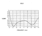
- FIG. 5 is a drawing showing frequency characteristics of VSWR in an embodiment of the slot antenna according to the present invention.
- FIG. 6 is a drawing showing frequency characteristics of return loss in an embodiment of the slot antenna according to the present invention.
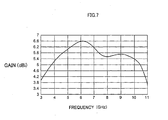
- FIG. 7 is a drawing showing frequency characteristics of gain in an embodiment of the slot antenna according to the present invention.
- FIG. 8 is a drawing showing radiation characteristics of frequency 4 GHz in an embodiment according to the slot antenna of the present invention.
- FIG. 9 is a drawing showing radiation characteristics of frequency 5 GHz in an embodiment of the slot antenna according to the present invention.
- FIG. 10 is a drawing showing radiation characteristics of frequency 6 GHz in an embodiment of the slot antenna according to the present invention.
- FIG. 11 is a drawing showing radiation characteristics of frequency 7 GHz in an embodiment of the slot antenna according to the present invention.
- FIG. 12 is a drawing showing radiation characteristics of frequency 8 GHz in an embodiment of the slot antenna according to the present invention.
- FIG. 13 is a drawing showing radiation characteristics of frequency 9 GHz in an embodiment of the slot antenna according to the present invention.
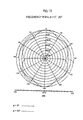
- FIG. 14 is a drawing showing radiation characteristics of frequency 10 GHz in an embodiment of the slot antenna according to the present invention.
- FIG. 15 is a drawing showing the three-dimensional radiation pattern at frequency 6.9 GHz of an embodiment of the slot antenna according to the present invention.
- FIG. 16 is a drawing of a prior art slot antenna.
- FIG.1 is an embodiment of the slot antenna according to the present invention.
- FIG. 1 (a) is a plane view of the slot antenna.
- FIG. 1 (b) is a cross sectional view cut at A-A' of the slot antenna.
- FIG. 1 (c) is a cross sectional view cut at B-B' of the slot antenna.
- a metal layer 11 in FIG. 1 is layered on an insulation substrate 10.
- the substrate 10 is composed of, for example, Teflon or FR-4.
- the metal layer 11 is comprised of one of Cu, Al, Au, or Pt for example.
- a slot is formed in the metal layer 11.
- the figure of the slot 12 is like a bow-tie shape as shown in FIG. 1 (a), and made inside the slot is an extension part 151 extending from a side of the slot antenna.
- slot 12' is narrowed step by step along the extension part 151. Narrowing it by three steps is an example. More steps or fewer steps are possible to narrow the slot, or the narrowing is possible.
- Four cut portions 14 are formed at each pointed edge of the slot 12.
- a feeding part 16 is comprised on the back side of the surfaces of substrate 10.
- the feeding part 16 is made of metal chosen from, for example, Cu, Al, Au, Ag or Pt.
- the feeding part 16 and the metal layer 11 are connected to each other via the through-hole of the substrate 10.
- a metal of the same type as the metal layer 11 is layered on the inner wall of the through-hole 15, and the through-hole is filled with the same insulator as the substrate10 or a different insulator from the substrate 10.
- a pin is inserted in the hole 15 to connect the metal layer 11 to the feeding part 16, as another example of the structure of the through-hole.
- the location of the through-hole is set near the end of the extension part 151 to make the slot antenna match with the feeding part 16.
- a rectangular x-y coordinate is defined as shown on FIG. 1 (a).
- the figure of the slot is symmetry of the y-axis, and an origin is defined at the center of the slot antenna on the y-axis.
- the width of the slot 12 in the direction of the y-axis is gradually enlarged in proportion to enlargement of the absolute value of the x-axis.
- the shape of the slot 12 is formed to be a bow-tie shape as shown in FIG. 1, and symmetric of the y-axis.
- the through-hole 15 is made near an end of the extension part 151 on the symmetry line.
- the slot antenna is connected to the feeding part 16 via the through-hole 15.
- the portion of the slot 12' adjacent to the extension part 151 is narrowed step by step along the extension part 151.
- the feeding part 16 is connected to a transmission circuit or a receiving circuit of a wireless device (not shown). Electric power fed from the transmission circuit to the metal layer 11 is radiated in the air. Electric power of radio wave is received by the metal layer 11 and transmitted to the receiving circuit connected to the feeding part 16.
- Preferred embodiments of the present invention achieve a slot antenna having excellent antenna characteristics in the ultra wide frequency band of UWB because of the slot bow-tie shape and the gradually narrowed slot along the extension part 151. Moreover, the best impedance matching can be accomplished easily by adjusting the through-hole location on the y axis.
- the slot antenna according to preferred embodiments of the present invention has profiles of low height, light weight, small size, easy fabrication, and low cost, so that the slot antenna according to such preferred embodiments of the present invention can be used in almost all portable wireless devices, including UWB systems with simple structures.
- FIG. 2A and FIG. 2B are embodiments of the through-hole connecting the metal layer 11 and the feeding part 16.
- FIG. 2A is a structure of through-hole formed by an electric conductive pin plugged in the substrate 10.
- the material of the pin is chosen from, for example, Cu, Al, Au, Ag or Pt.
- FIG. 2B (a) is a cross sectional view of the substrate 10, and FIG. 2B (b) is a plane view of the backside of the substrate 10.
- an electrically conductive film 152 is deposited on the inner wall of the through-hole 15 and insulator 153 is filled in the hole.
- FIG. 3 is another example of a slot antenna according to an embodiment of the present invention.
- the outer form of the metal layer 11 is a rectangle of 20 mm x 44 mm.
- the outer form of metal layer 11 is 44 mm x 20 mm.
- the width of the slot 12 is 40 mm, and the longitudinal length of the slot is 16 mm.
- the slot antenna is symmetric with respect to the y-axis.
- An origin O of the x-y coordinate system is defined as the center of the rectangle of the outer lines of metal layer 11.
- the through-hole 15 is formed on the y-axis and near the end of the extension part 151 extending into slot 12.
- the extension part 151 with a width of 2 mm x a length of 8 mm and the feeding part 16 are connected with the through-hole 15.
- the distances between the sides along the extension part 151 are 6 mm, 4 mm and 3.2 mm.
- the smallest width of the slot along the extension part 151 is 0.8 mm.
- the length of the cut portions 14 made at the pointed edges of the slot is 1 mm.
- the feeding part 16 and the through-hole 15 are explained in detail referring to FIG. 4.
- the metallic layer 11 is copper of 0.018 mm thickness.
- the pattern of slot 12 is made, for example, by photo-etching the copper film layered on the substrate.
- the copper layer of the substrate is eliminated by photo-etching techniques to make the slot pattern.
- the slot pattern can be made by printing electric-conductive paste of copper on the substrate.
- the feeding part of Cu can be made, for example, by printing electric-conducting paste containing copper.
- the feeding part may also be made by photo-etching copper film layered on the substrate.
- the feeding part 16 is copper of 0.018 mm thickness.
- the substrate 10 in addition to Teflon, various kinds of other materials can be used such as FR-4. Parameters like permittivity, loss tan ä, the thickness of the substrate, size, etc. are determined according to antenna size and antenna characteristics.
- FIG. 4 is an example of feeding part 16 and the through-hole location of the slot antenna according to an embodiment of the present invention.
- the feeding part 16 is formed on the back side of the substrate 10.
- the lower part of the slot (A-A') (shown in FIG. 3) on the front side of substrate 10 is aligned to a side of feed point line A-A' on the back side of the substrate 10 in FIG. 4.
- the feeding part 16 is a T-shape transmission line as shown in FIG. 4.
- the feeding part is T shaped for impedance matching with a 50-ohm connector.
- the width of the T-shape is decided to have impedance of 50 ohms to connect to a connector (not shown).
- the length of longitudinal part b of the T shape is designed to impedance match with the slot antenna on the front side of the substrate 10.
- the feeding part 16 is connected to the metal layer 11 by the copper layer 152 on the inner wall of the through-hole 15.
- the through-hole 15 is plugged with an insulation material 153, which is, for example, the same material as the substrate 10 such as Teflon or FR-4.
- FIG. 5 - FIG. 15 show antenna characteristics of the designed slot antenna shown in FIG. 3 and FIG. 4.
- the simulation results have been obtained from two different software programs, Ansoft Designer and HFSS (High Frequency Structure Simulator). Because the results of the simulators are the same, the obtained results appear to be accurate.
- FIG. 5 is VSWR characteristics in the entire frequency band from 3.5 GHz to 10.6 GHz. As shown in FIG. 5, the designed antenna has VSWR less than 2.5:1 from frequency of 3.5-10.6 GHz.
- FIG. 6 is return loss characteristic in the entire frequency band from 3.5 GHz to 10.6 GHz. As shown in FIG.6, the designed antenna has a return loss of -7 dB in the entire frequency range from 3.5 GHz to 10.6 GHz.
- FIG. 7 is gain characteristics in the entire frequency band from 3.5 GHz to 10.6 GHz. As shown in FIG. 7, the designed antenna achieves more than 4 dBi gain in the entire frequency from 3.5 GHz to 10.6 GHz.
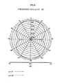
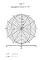
- FIG. 8 is the radiation pattern of 4 GHz.
- FIG. 9 is the radiation pattern of 5 GHz.
- FIG. 10 is the radiation pattern of 6 GHz.
- FIG. 11 is the radiation pattern of 7 GHz.
- FIG. 12 is the radiation pattern of 8 GHz.
- FIG. 13 is the radiation pattern of 9 GHz.
- FIG. 14 is the radiation pattern of 10 GHz.
- the radiation patterns of frequency from 4 GHz to 10 GHz are almost the same patterns.
- the results prove that the slot antenna of the present invention is very effective for use with UWB wireless devices with high data rates and low power densities.
- FIG. 15 is a three-dimensional radiation pattern according to embodiments of the present invention.
- the origin of the axis is the same as that defined in FIG. 3.
- the z axis is defined perpendicular to the x-y plane at the origin.
- the radiation pattern is uniform in space in three dimensions. This pattern proves that the slot antenna of such embodiments of the present invention is excellent and effective for use in UWB wireless communication systems.
Landscapes
- Waveguide Aerials (AREA)
- Details Of Aerials (AREA)
Abstract
Description
Claims (8)
- A slot antenna comprising:an insulation substrate;a metal layer on the insulation substrate; anda feeding part connected to the metal layer, whereinthe metal layer has a slot,the slot is symmetric with respect to a centerline, andwhen an x-y coordinate system is defined on the metal layer so that the y-axis is the centerline, the origin is the center of the slot antenna, and the x-axis through the origin is perpendicular to the y-axis, the width of the slot in the direction of the y-axis is gradually enlarged in proportion to the absolute value of the x-axis.
- The slot antenna of claim 1, wherein:the shape of the slot is a bow-tie type;an extension part extends on the centerline from a side of the slot antenna into the slot; andthe feeding part is connected at an end of the extension part.
- The slot antenna of claim 2, wherein the slot along the extension part is narrowed gradually.
- The slot antenna of claim 1, wherein:the metal layer of the slot antenna is formed on a front side of the insulation substrate;the feeding part is formed on a back side of the insulation substrate;the insulation substrate has a hole from the front side to the back side;an electric conducting layer is formed on the inner surface of the hole or an electric conductive pin is inserted in the hole; andthe feeding part is connected to the metal layer by the electric conducting layer or by the electric conductive pin.
- The slot antenna of claim 2, wherein:the metal layer of the slot antenna is formed on a front side of the insulation substrate;the feeding part is formed on a back side of the insulation substrate;the insulation substrate has a hole from the front side to the back side;an electric conducting layer is formed on the inner surface of the hole or an electric conductive pin is inserted in the hole; andthe feeding part is connected to the metal layer by the electric conductive layer or by the electric conductive pin.
- The slot antenna of claim 1, comprising a cut portion at each end of the sides of the slot parallel to the y-axis.
- The slot antenna of claim 1, wherein:the metal layer is made of one of Cu, Au, Ag, or Pt; andthe feeding part is made of one of Cu, Au, Ag, or Pt.
- The slot antenna of claim 1, wherein the insulation layer is made of Teflon or FR-4.
Applications Claiming Priority (2)
| Application Number | Priority Date | Filing Date | Title |
|---|---|---|---|
| JP2004043395 | 2004-02-19 | ||
| JP2004043395A JP2005236672A (en) | 2004-02-19 | 2004-02-19 | Bowtie slot antenna |
Publications (2)
| Publication Number | Publication Date |
|---|---|
| EP1566858A1 true EP1566858A1 (en) | 2005-08-24 |
| EP1566858B1 EP1566858B1 (en) | 2008-07-30 |
Family
ID=34709126
Family Applications (1)
| Application Number | Title | Priority Date | Filing Date |
|---|---|---|---|
| EP04030241A Expired - Lifetime EP1566858B1 (en) | 2004-02-19 | 2004-12-21 | Ultra wideband bow-tie slot antenna |
Country Status (4)
| Country | Link |
|---|---|
| US (1) | US7193576B2 (en) |
| EP (1) | EP1566858B1 (en) |
| JP (1) | JP2005236672A (en) |
| DE (1) | DE602004015404D1 (en) |
Cited By (3)
| Publication number | Priority date | Publication date | Assignee | Title |
|---|---|---|---|---|
| GB2448551A (en) * | 2007-04-20 | 2008-10-22 | Iti Scotland Ltd | Ultra-wideband antenna |
| CN1925224B (en) * | 2005-08-31 | 2012-06-20 | 日立电线株式会社 | Wideband antenna |
| WO2019007444A3 (en) * | 2018-03-23 | 2019-03-07 | 罗森伯格技术(昆山)有限公司 | Antenna wiring sleeve, and antenna assembly provided with wiring sleeve |
Families Citing this family (27)
| Publication number | Priority date | Publication date | Assignee | Title |
|---|---|---|---|---|
| USD347612S (en) * | 1991-05-20 | 1994-06-07 | Allen Dillis V | Steering wheel assembly with communication keyboard |
| JP4268585B2 (en) * | 2004-12-20 | 2009-05-27 | アルプス電気株式会社 | Antenna device |
| JP2007074226A (en) * | 2005-09-06 | 2007-03-22 | Alps Electric Co Ltd | Vehicle-mounted antenna system |
| US7388550B2 (en) * | 2005-10-11 | 2008-06-17 | Tdk Corporation | PxM antenna with improved radiation characteristics over a broad frequency range |
| US7450077B2 (en) * | 2006-06-13 | 2008-11-11 | Pharad, Llc | Antenna for efficient body wearable applications |
| US7453402B2 (en) * | 2006-06-19 | 2008-11-18 | Hong Kong Applied Science And Research Institute Co., Ltd. | Miniature balanced antenna with differential feed |
| TWM318203U (en) * | 2007-01-19 | 2007-09-01 | Smart Ant Telecom Co Ltd | Dipole array directional antenna |
| USD604275S1 (en) * | 2007-04-20 | 2009-11-17 | Iti Scotland Limited | Antenna |
| ATE547824T1 (en) * | 2007-10-16 | 2012-03-15 | Hirschmann Car Comm Gmbh | METHOD FOR PRODUCING A VEHICLE ANTENNA DEVICE |
| US9105966B1 (en) * | 2010-08-17 | 2015-08-11 | Amazon Technologies, Inc. | Antenna with an exciter |
| TW201310766A (en) * | 2011-08-26 | 2013-03-01 | Yong-Kang Lv | Directional digital TV antenna |
| US9679828B2 (en) | 2012-01-31 | 2017-06-13 | Amit Verma | System-on-chip electronic device with aperture fed nanofilm antenna |
| TWI506859B (en) * | 2013-11-08 | 2015-11-01 | Nat Univ Chin Yi Technology | Coplanar waveguide (cpw-fed) antenna applied in 2g, 3g and 4g systems |
| USD802563S1 (en) * | 2014-08-21 | 2017-11-14 | Vorbeck Materials Corp. | Radio frequency identification antenna |
| US9899741B2 (en) * | 2015-01-26 | 2018-02-20 | Rodradar Ltd. | Radio frequency antenna |
| USD766882S1 (en) * | 2015-05-07 | 2016-09-20 | Airgain Incorporated | Antenna |
| USD784965S1 (en) * | 2015-07-10 | 2017-04-25 | Airgain Incorporated | Antenna |
| USD795228S1 (en) * | 2016-03-04 | 2017-08-22 | Airgain Incorporated | Antenna |
| USD795847S1 (en) * | 2016-03-08 | 2017-08-29 | Airgain Incorporated | Antenna |
| USD801318S1 (en) * | 2016-04-05 | 2017-10-31 | Vorbeck Materials Corp. | Antenna inlay |
| TWI643406B (en) * | 2017-07-14 | 2018-12-01 | 緯創資通股份有限公司 | Antenna structure |
| US11121474B2 (en) | 2017-11-10 | 2021-09-14 | Raytheon Company | Additive manufacturing technology (AMT) low profile radiator |
| CN108777364A (en) * | 2018-06-11 | 2018-11-09 | 中国计量大学 | For tri- frequency channel microstrip antenna of WiFi, WiMAX and WLAN |
| CN108832300A (en) * | 2018-06-25 | 2018-11-16 | 英华达(上海)科技有限公司 | Antenna assembly |
| WO2021124844A1 (en) * | 2019-12-20 | 2021-06-24 | コニカミノルタ株式会社 | Antenna device and tag reader |
| CN112467351B (en) * | 2020-11-19 | 2022-04-19 | 中国电子科技集团公司第二十九研究所 | A multi-resonant excitation cavity-backed antenna |
| CN113093117B (en) * | 2021-06-03 | 2021-09-07 | 成都雷电微晶科技有限公司 | Millimeter wave single-channel control TR component |
Citations (5)
| Publication number | Priority date | Publication date | Assignee | Title |
|---|---|---|---|---|
| US6429819B1 (en) * | 2001-04-06 | 2002-08-06 | Tyco Electronics Logistics Ag | Dual band patch bowtie slot antenna structure |
| EP1229605A1 (en) * | 2001-02-02 | 2002-08-07 | Intracom S.A. Hellenic Telecommunications & Electronics Industry | Wideband printed antenna system |
| US20020154064A1 (en) * | 1997-09-09 | 2002-10-24 | Time Domain Corporation | Ulta-wideband magnetic antenna |
| US20020180654A1 (en) * | 1999-12-22 | 2002-12-05 | Olivier Acher | Anisotripic composite antenna |
| US20030043084A1 (en) * | 2001-09-03 | 2003-03-06 | Yoshimi Egashira | Slotted bow tie antenna with parasitic element, and slotted bow tie array antenna with parasitic element |
Family Cites Families (21)
| Publication number | Priority date | Publication date | Assignee | Title |
|---|---|---|---|---|
| US2935747A (en) * | 1956-03-05 | 1960-05-03 | Rca Corp | Broadband antenna system |
| DE2949013C2 (en) * | 1979-12-06 | 1985-05-02 | ANT Nachrichtentechnik GmbH, 7150 Backnang | Transition from a coaxial cable to a multi-pin connector |
| US4607394A (en) * | 1985-03-04 | 1986-08-19 | General Electric Company | Single balanced planar mixer |
| US5308250A (en) * | 1992-10-30 | 1994-05-03 | Hewlett-Packard Company | Pressure contact for connecting a coaxial shield to a microstrip ground plane |
| JPH06303010A (en) | 1993-04-14 | 1994-10-28 | Sony Corp | High frequency transmission line, integrated circuit device using the high frequency transmission line, and method of connecting high frequency plane circuit |
| JP2829378B2 (en) | 1995-08-17 | 1998-11-25 | 郵政省通信総合研究所長 | Superconductor electromagnetic wave generation method and device |
| JPH09246817A (en) | 1996-03-08 | 1997-09-19 | Nippon Telegr & Teleph Corp <Ntt> | RF power divider / combiner |
| JP3883251B2 (en) | 1997-04-18 | 2007-02-21 | 九州電力株式会社 | Radar antenna |
| JP3580667B2 (en) | 1997-05-28 | 2004-10-27 | 京セラ株式会社 | Conversion line |
| US6211840B1 (en) * | 1998-10-16 | 2001-04-03 | Ems Technologies Canada, Ltd. | Crossed-drooping bent dipole antenna |
| JP2001345608A (en) | 2000-06-05 | 2001-12-14 | Toyota Central Res & Dev Lab Inc | Line converter |
| JP2002111208A (en) | 2000-09-29 | 2002-04-12 | Nippon Telegr & Teleph Corp <Ntt> | Multilayer dielectric substrate |
| JP2002135037A (en) | 2000-10-26 | 2002-05-10 | Mitsubishi Electric Corp | Bowtie antenna |
| JP3830358B2 (en) | 2001-03-23 | 2006-10-04 | 日立電線株式会社 | Flat antenna and electric device having the same |
| JP2002353726A (en) | 2001-05-29 | 2002-12-06 | Furukawa Electric Co Ltd:The | Small antenna |
| JP2003078345A (en) | 2001-09-03 | 2003-03-14 | Sansei Denki Kk | Slot-type bowtie antenna device and method of configuring the same |
| JP3502945B2 (en) | 2001-10-05 | 2004-03-02 | オムロン株式会社 | Radio wave sensor |
| JP2003174315A (en) | 2001-12-05 | 2003-06-20 | Alps Electric Co Ltd | Monopole antenna |
| JP2003283241A (en) | 2002-03-27 | 2003-10-03 | Mitsubishi Electric Corp | Microstrip antenna |
| US6975258B2 (en) | 2003-01-23 | 2005-12-13 | Corporation For National Research Initiatives | Circuit for direct digital delta-sigma conversion of variable electrical capacitance |
| US6975278B2 (en) * | 2003-02-28 | 2005-12-13 | Hong Kong Applied Science and Technology Research Institute, Co., Ltd. | Multiband branch radiator antenna element |
-
2004
- 2004-02-19 JP JP2004043395A patent/JP2005236672A/en active Pending
- 2004-12-21 DE DE602004015404T patent/DE602004015404D1/en not_active Expired - Lifetime
- 2004-12-21 EP EP04030241A patent/EP1566858B1/en not_active Expired - Lifetime
- 2004-12-29 US US11/023,454 patent/US7193576B2/en not_active Expired - Fee Related
Patent Citations (5)
| Publication number | Priority date | Publication date | Assignee | Title |
|---|---|---|---|---|
| US20020154064A1 (en) * | 1997-09-09 | 2002-10-24 | Time Domain Corporation | Ulta-wideband magnetic antenna |
| US20020180654A1 (en) * | 1999-12-22 | 2002-12-05 | Olivier Acher | Anisotripic composite antenna |
| EP1229605A1 (en) * | 2001-02-02 | 2002-08-07 | Intracom S.A. Hellenic Telecommunications & Electronics Industry | Wideband printed antenna system |
| US6429819B1 (en) * | 2001-04-06 | 2002-08-06 | Tyco Electronics Logistics Ag | Dual band patch bowtie slot antenna structure |
| US20030043084A1 (en) * | 2001-09-03 | 2003-03-06 | Yoshimi Egashira | Slotted bow tie antenna with parasitic element, and slotted bow tie array antenna with parasitic element |
Non-Patent Citations (1)
| Title |
|---|
| ELDEK A A ET AL: "Wideband slot antennas for radar applications", PROCEEDINGS OF THE 2003 IEEE RADAR CONFERENCE. HUNTSVILLE, AL, MAY 5 - 8, 2003, IEEE RADAR CONFERENCE, NEW YORK, NY : IEEE, US, 5 May 2003 (2003-05-05), pages 79 - 84, XP010642644, ISBN: 0-7803-7920-9 * |
Cited By (6)
| Publication number | Priority date | Publication date | Assignee | Title |
|---|---|---|---|---|
| CN1925224B (en) * | 2005-08-31 | 2012-06-20 | 日立电线株式会社 | Wideband antenna |
| GB2448551A (en) * | 2007-04-20 | 2008-10-22 | Iti Scotland Ltd | Ultra-wideband antenna |
| WO2008129262A3 (en) * | 2007-04-20 | 2009-05-07 | Iti Scotland Ltd | Ultra wideband antenna |
| GB2448551B (en) * | 2007-04-20 | 2010-03-31 | Iti Scotland Ltd | Ultra wideband antenna |
| WO2019007444A3 (en) * | 2018-03-23 | 2019-03-07 | 罗森伯格技术(昆山)有限公司 | Antenna wiring sleeve, and antenna assembly provided with wiring sleeve |
| US11296396B2 (en) | 2018-03-23 | 2022-04-05 | Rosenberger Technology (Kunshan) Co., Ltd | Antenna wiring sleeve, and antenna assembly provided with wiring sleeve |
Also Published As
| Publication number | Publication date |
|---|---|
| DE602004015404D1 (en) | 2008-09-11 |
| JP2005236672A (en) | 2005-09-02 |
| US7193576B2 (en) | 2007-03-20 |
| EP1566858B1 (en) | 2008-07-30 |
| US20050184919A1 (en) | 2005-08-25 |
Similar Documents
| Publication | Publication Date | Title |
|---|---|---|
| US7193576B2 (en) | Ultra wideband bow-tie slot antenna | |
| EP1515396B1 (en) | Ultra wideband bow-tie printed antenna | |
| Angelopoulos et al. | Circular and elliptical CPW-fed slot and microstrip-fed antennas for ultrawideband applications | |
| US7804456B2 (en) | Ultra wideband loop antenna | |
| US6429819B1 (en) | Dual band patch bowtie slot antenna structure | |
| Naktong et al. | Four-port rectangular monopole antenna for UWB-MIMO applications | |
| US20100295750A1 (en) | Antenna for diversity applications | |
| Shanmugam | Design and analysis of a frequency reconfigurable penta-band antenna for WLAN and 5G applications | |
| CN110474161A (en) | A slot-loaded ultra-wideband antenna with microstrip structure | |
| KR100535255B1 (en) | Small planar antenna with ultra wide bandwidth and manufacturing method thereof | |
| KR100674200B1 (en) | Multiple shock-slot microstrip patch antenna | |
| EP1276170B1 (en) | Multi-band antenna | |
| US20080316108A1 (en) | Compact Antennas for Ultra-Wideband Applications | |
| Yazdandoost et al. | Bow-tie antenna for UWB communication frequency | |
| Chair et al. | Comparative study on the mutual coupling between different sized cylindrical dielectric resonators antennas and circular microstrip patch antennas | |
| Geng et al. | A novel miniaturized Vivaldi antenna for ultra-wideband applications | |
| US11342678B1 (en) | Dual polarized MIMO UWB system: a method and device thereof | |
| Su et al. | A bent, shorted, planar monopole antenna for 2.4 GHz WLAN applications | |
| CN108258409A (en) | A kind of wing terminal octagon gap three-frequency plane slot antenna | |
| Yazdandoost et al. | Slot antenna for ultra wideband system | |
| Nafilah et al. | Design and implementation of Vivaldi antenna with modified Marchand balun for V2X communications | |
| Rahayu et al. | A small novel ultra wideband antenna with slotted ground plane | |
| Moutaouakil et al. | Design and simulation of a fractal multiband antenna printed on a circular patch | |
| Jin et al. | A novel two-layer stacked microstrip antenna array using cross snowflake fractal patches | |
| Harbadji et al. | Triple band Compact Fractal Antenna with Defected Ground Plane for Bluetooth, WiMAX, and WLAN Applications |
Legal Events
| Date | Code | Title | Description |
|---|---|---|---|
| PUAI | Public reference made under article 153(3) epc to a published international application that has entered the european phase |
Free format text: ORIGINAL CODE: 0009012 |
|
| AK | Designated contracting states |
Kind code of ref document: A1 Designated state(s): AT BE BG CH CY CZ DE DK EE ES FI FR GB GR HU IE IS IT LI LT LU MC NL PL PT RO SE SI SK TR |
|
| AX | Request for extension of the european patent |
Extension state: AL BA HR LV MK YU |
|
| 17P | Request for examination filed |
Effective date: 20060123 |
|
| AKX | Designation fees paid |
Designated state(s): DE FI FR GB |
|
| 17Q | First examination report despatched |
Effective date: 20060310 |
|
| GRAP | Despatch of communication of intention to grant a patent |
Free format text: ORIGINAL CODE: EPIDOSNIGR1 |
|
| GRAS | Grant fee paid |
Free format text: ORIGINAL CODE: EPIDOSNIGR3 |
|
| GRAA | (expected) grant |
Free format text: ORIGINAL CODE: 0009210 |
|
| AK | Designated contracting states |
Kind code of ref document: B1 Designated state(s): DE FI FR GB |
|
| REG | Reference to a national code |
Ref country code: GB Ref legal event code: FG4D |
|
| REF | Corresponds to: |
Ref document number: 602004015404 Country of ref document: DE Date of ref document: 20080911 Kind code of ref document: P |
|
| PLBE | No opposition filed within time limit |
Free format text: ORIGINAL CODE: 0009261 |
|
| STAA | Information on the status of an ep patent application or granted ep patent |
Free format text: STATUS: NO OPPOSITION FILED WITHIN TIME LIMIT |
|
| 26N | No opposition filed |
Effective date: 20090506 |
|
| PGFP | Annual fee paid to national office [announced via postgrant information from national office to epo] |
Ref country code: FR Payment date: 20110107 Year of fee payment: 7 |
|
| PGFP | Annual fee paid to national office [announced via postgrant information from national office to epo] |
Ref country code: FI Payment date: 20101220 Year of fee payment: 7 |
|
| PGFP | Annual fee paid to national office [announced via postgrant information from national office to epo] |
Ref country code: GB Payment date: 20101221 Year of fee payment: 7 |
|
| PGFP | Annual fee paid to national office [announced via postgrant information from national office to epo] |
Ref country code: DE Payment date: 20101229 Year of fee payment: 7 |
|
| GBPC | Gb: european patent ceased through non-payment of renewal fee |
Effective date: 20111221 |
|
| PG25 | Lapsed in a contracting state [announced via postgrant information from national office to epo] |
Ref country code: FI Free format text: LAPSE BECAUSE OF NON-PAYMENT OF DUE FEES Effective date: 20111221 |
|
| REG | Reference to a national code |
Ref country code: FR Ref legal event code: ST Effective date: 20120831 |
|
| REG | Reference to a national code |
Ref country code: DE Ref legal event code: R119 Ref document number: 602004015404 Country of ref document: DE Effective date: 20120703 |
|
| PG25 | Lapsed in a contracting state [announced via postgrant information from national office to epo] |
Ref country code: GB Free format text: LAPSE BECAUSE OF NON-PAYMENT OF DUE FEES Effective date: 20111221 Ref country code: DE Free format text: LAPSE BECAUSE OF NON-PAYMENT OF DUE FEES Effective date: 20120703 |
|
| PG25 | Lapsed in a contracting state [announced via postgrant information from national office to epo] |
Ref country code: FR Free format text: LAPSE BECAUSE OF NON-PAYMENT OF DUE FEES Effective date: 20120102 |