CROSS-REFERENCE TO RELATED APPLICATION
This application claims priority to and the benefit of Korean Patent
Application No. 2004-5154, filed January 27, 2004, the disclosure of which is
incorporated by reference in its entirety.
BACKGROUND OF THE INVENTION
1. Field of the Invention
The present invention relates to an organic light emitting display and
method of fabricating the same and, more particularly, to an organic light
emitting display and method of fabricating the same in which surface corners of
a connection hole are formed to be curved which is formed between upper and
lower conductive layers to interconnect the upper conductive layer and the
lower conductive layer so that short-circuit failures may be reduced.
2. Description of the Related Art
In recent years, development for an active matrix organic light emitting
display (AMOLED) as an active matrix flat panel display using an organic light
emitting (EL) diode is being progressed, which is applied to a cellular phone or
the like, so that thickness and size thereof are remarkably reduced,
manufacturing cost is reduced and a process thereof is also simplified.
FIG. 1A is a plan view of a conventional organic light emitting display.
The organic light emitting display of FIG. 1A is illustrated to consist of two
transistors and one capacitor.
FIG. 1B is a cross-sectional view taken along the line I-I of FIG. 1A.
Referring to FIG. 1B, the conventional organic light emitting display has an
emission region 130 where a lower electrode 131 as a pixel electrode, an
organic emission layer 132 and a upper electrode 133 are formed, and a non-emission
region 110 where two thin film transistors (TFT) and a capacitor are
formed.
In the non-emission region 110, a buffer layer 140 is formed on a
transparent insulating substrate 100 such as a glass substrate, and amorphous
silicon is deposited on the buffer layer 140, and then patterned and crystallized
to form a semiconductor layer 111. A gate insulating layer 150 is then formed
on the entire surface of the substrate, and a metal material for forming a gate
electrode is deposited on the gate insulating layer 150 and then patterned to
form a gate 112 on the semiconductor layer 111, while a capacitor bottom
electrode 122 is formed. In this case, a gate line 102 shown in FIG. 1A is
simultaneously formed while the gate 112 and the capacitor lower electrode 122
are formed.
Subsequently, impurities having a predetermined conductivity type such
as a P type or an N type are ion-implanted into the semiconductor layer 111 to
form source and drain regions 113 and 114.
An inter-insulating layer 160 is then formed on the entire surface of the
substrate, and the inter-insulating layer 160 and the gate insulating layer 150
are etched so as to expose portions of the source and drain regions 113 and
114 to thereby form contact holes 161 and 162 for source and drain electrodes.
Subsequently, a metal material for forming the source and drain
electrodes is deposited on the inter-insulating layer 160 to form the source and
drain electrodes 115 and 116 which are in contact with the source and drain
regions 113 and 114 through the contact holes 161 and 162, respectively. In
this case, a capacitor top electrode 126 which extends from one electrode of the
source and drain electrodes 115 and 116, for example, the drain electrode 116,
is formed while a data line 104 and a power supply line 106 shown in FIG. 1A
are formed.
A passivation layer 170 is then formed on the inter-insulating layer 160.
The passivation layer 170 is etched so as to expose a portion of the other
electrode of the source and drain electrodes 115 and 116, for example, the
source electrode 115 to thereby form a contact hole 171 for a pixel electrode.
A transparent conductive layer is deposited on the passivation layer 170
of the emission region 130 and then patterned to form a bottom electrode 131
which is in contact with the source electrode 115 through the contact hole 171
for the pixel electrode.
An insulating layer 180 for planarization is formed on the passivation
layer 170, and an opening 181 is formed so as to expose the lower electrode
131. An organic emission layer 132 is formed on the planarization layer 180
including the opening 181, and a top electrode 133 is formed thereon.
When a taper angle of the contact hole of the conventional organic light
emitting display having the above-described configuration is large, pin-hole
failures occurred at a stepped portion near the contact hole.
To cope with such a problem, taper angles at edge portions of the
contact holes 161, 162, and 171 are alleviated to prevent the failures from
occurring.
A process of forming the contact hole of the conventional organic light
emitting display in which the taper angle is alleviated will be described with
reference to FIGs. 1C to 1F.
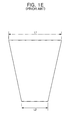
FIG. 1C is a perspective view illustrating a shape of the contact holes
161, 162, and 171, FIG. 1D is a plan view of the contact holes 161, 162, and
171, and FIG. 1E is a cross-sectional view taken along the line II-II of FIG. 1C.
Referring to FIGs. 1C to 1E, corners of top and bottom surfaces of each
of the contact holes 161, 162, and 171 are angled, and the length L1 of the top
surface of each of the contact holes 161, 162, and 171 is formed to be larger
than the length L2 of the bottom surface of each of the contact holes 161, 162,
and 171.
That is, the contact holes 161, 162, and 171 are formed to have inclined
sides so as to have taper angles.
The pin-hole failures may be reduced to some extent by means of the
alleviated taper angle, however, a short-circuit failure may occur due to an edge
open at the angled corner on the surface in the conventional organic light
emitting display.
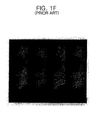
FIG. 1F is an enlarged view of an emission region when the short-circuit
failure occurred, wherein problematic dark spots may occur at the corners of the
contact holes 161, 162, and 171 when the short-circuit failures occur.
SUMMARY OF THE INVENTION
The present invention, therefore, solves aforementioned problems
associated with conventional devices by providing an organic light emitting
display and method of fabricating the same in which surface corner portions of
contact holes and via holes are formed to be curved to reduce the short-circuit
failures.
The present invention also provides an organic light emitting display
allowing durability to be lengthened and image quality to be enhanced.
In an exemplary embodiment of the present invention, an organic light
emitting display includes: a semiconductor layer formed on a substrate, and
having source and drain regions; a thin film transistor formed on the substrate,
and having source and drain electrodes electrically connected to the
semiconductor layer through a connection hole; a lower electrode formed on an
emission region of the substrate, and connected to one electrode of the source
and drain electrodes through a connection hole; an organic emission layer
formed on the emission region of the lower electrode; and a upper electrode
formed on the organic emission layer, wherein of the connection hole has a
curved surface corner portion.
A corner of a bottom surface of the connection hole may have a
curvature; a center of the curvature may be present on the bottom surface; a
top surface of the connection hole may have a point which is positioned on the
same axis vertically extending from a surface including a center of a radius of
curvature of the bottom surface, as a center of a radius of curvature; the radius
of curvature of the top surface of the connection hole may be larger than that of
the bottom surface; and all of the curvature of the top surface and the curvature
of the bottom surface of the connection hole may be formed at respective four
corners.
Corners of the top and bottom surfaces of the connection hole may be
circular; a point positioned on the same axis vertically extending from a surface
including the center of the radius of the top surface may be the center of the
radius of the bottom surface; the radius of the top surface of the connection hole
may be larger than that of the bottom surface; a connection hole formed on the
insulating layer to insulate the source and drain regions from the source and
drain electrodes may serve as a contact hole; and a connection hole formed on
the insulating layer to insulate the source and drain electrodes from the lower
electrode may serve as a via hole. The lower electrode may be an anode
electrode.
In another exemplary embodiment according to the present invention, a
method of fabricating an organic light emitting display includes: forming a
semiconductor layer having source and drain regions on a substrate; forming a
thin film transistor provided with source and drain electrodes electrically
connected to the semiconductor layer through a connection hole on the
substrate; forming a lower electrode connected to one electrode of the source
and drain electrodes through a connection hole on an emission region of the
substrate; forming an organic emission layer on the emission region of the lower
electrode; and forming a upper electrode on the organic emission layer, wherein
the connection hole has a curved surface corner portion.
A corner of a bottom surface of the connection hole may have a
curvature; a center of the curvature may be is present on the bottom surface; a
top surface of the connection hole may have a point which is positioned on the
same axis vertically extending from a surface including a center of a radius of
curvature of the bottom surface, as a center of a radius of curvature; the radius
of curvature of the top surface of the connection hole may be formed to be
larger than that of the bottom surface; and all of the curvature of the top surface
and the curvature of the bottom surface of the connection hole may be formed
at respective four corners.
Corners of the top and bottom surfaces of the connection hole may be
formed to be circular; a point positioned on the same axis vertically extending
from a surface including the center of the radius of the top surface may be the
center of the radius of the bottom surface; and the radius of the top surface of
the connection hole may be formed to be larger than that of the bottom surface.
BRIEF DESCRIPTION OF THE DRAWINGS
The above and other features of the present invention will be described
in reference to certain exemplary embodiments thereof with reference to the
attached drawings in which:
DETAILED DESCRIPTION OF THE INVENTION
The present invention will now be described more fully hereinafter with
reference to the accompanying drawings, in which preferred embodiments of
the invention are shown.
FIG. 2A is a plan view of an organic light emitting display in accordance
with a first embodiment of the present invention.
The organic light emitting display of FIG. 2A is illustrated to have two
transistors and one capacitor.
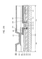
FIG. 2B is a cross-sectional view of an organic light emitting display
taken along the line III-III of FIG. 2A.
Referring to FIG. 2B, in a non-emission region 210 of the organic light
emitting display according to the first embodiment of the present invention, a
buffer layer 240 is formed on a transparent substrate 200 such as a glass
substrate, and amorphous silicon is deposited on the buffer layer 240, which is
then patterned and crystallized to form a semiconductor layer 211. A gate
insulating layer 250 is then formed on the entire surface of the substrate, and a
metal material for forming a gate electrode is deposited on the gate insulating
layer 250 and then patterned to form a gate 212 on the semiconductor layer 211,
while a capacitor bottom electrode 222 is formed. In this case, a gate line 202
shown in FIG. 2A is simultaneously formed while the gate 212 and the capacitor
bottom electrode 222 are formed.
Subsequently, impurities having a predetermined conductivity type such
as a P type or an N type are ion-implanted into the semiconductor layer 211 so
that source and drain regions 213 and 214 are formed.
An inter-insulating layer 260 is then formed on the entire surface of the
substrate, and the inter-insulating layer 260 and the gate insulating layer 250
are etched so as to expose some portions of the source and drain regions 213
and 214 to thereby form first and second connection holes 261 and 262 for
source and drain electrodes.
Subsequently, a metal material for forming source and drain electrodes
is deposited on the inter-insulating layer 260 to form the source and drain
electrodes 215 and 216 which are in contact with the source and drain regions
213 and 214 through the first and second connection holes 261 and 262,
respectively. In this case, a capacitor upper electrode 226 which extends from
one electrode of the source and drain electrodes 215 and 216, for example, the
drain electrode 216, is formed while a data line 204 and a power supply line 206
shown in FIG. 2A are formed.
A passivation layer 270 is then formed on the inter-insulating layer 260.
The passivation layer 270 is etched to expose a portion of the other electrode of
the source and drain electrodes 215 and 216, for example, the source electrode
215 to thereby form a third connection hole 271.
In this case, a process of forming the first to third connection holes
shown in FIG. 2A will be described with reference to FIGs. 2C to 2E.
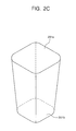
FIG. 2C is a perspective view illustrating a whole shape of each of the
first to third connection holes 261, 262, and 271, FIG. 2D is a plan view of the
first to third connection holes 261, 262, and 271, and FIG. 2E is a cross-sectional
view taken along the line IV-IV of FIG. 2D.
When the first to third connection holes 261, 262, and 271 are formed,
four corners of the planar top surface 261a are curved and four corners of the
bottom surface 261b are curved as shown in FIG. 2D, and the first to third
connection holes 261, 262, and 261 are formed to be tapered as shown in FIG.
2E, so that the top surface 261 a is formed to be wider than the bottom surface
261b.
This may be expressed as the equation below:
ρ 1 > ρ 2 > 0
where, ρ 1 indicates a radius of curvature of the top surface 261a of
the first to third connection holes 261, 262, and 271, and p 2 indicates a radius
of curvature of the bottom surface 261b of the first to third connection holes 261,
262, and 271.
Each of four corners of the bottom surface 261 b of the first to third
connection holes 261, 262, and 271 has a curvature, and a center of the radius
of curvature of the bottom surface 261 b is present on the bottom surface 261 b,
and the top surface 261 a of the first to third connection holes 261, 262, and 271
has a center of the radius of curvature (ρ 1) which is positioned on the same
axis vertically extending from the surface including the center of the radius of
curvature (ρ 2) of the bottom surface 261b, and the radius of curvature (ρ 1) of
the top surface 261 a of the first to third connection holes 261, 262, and 271 is
larger than the radius of curvature (ρ 2) of the bottom surface 261b, and not
only four corners of the bottom surface 261b of the first to third connection holes
261, 262, and 271 but also four corners of the top surface 261 a are curved, so
that a short-circuit failure caused by the edge open of the four corners may be
prevented.
A transparent conductive layer is then deposited on the passivation
layer 270 of the emission region 230 and then patterned to form a lower
electrode 231 which is in contact with the source electrode 215 through the third
connection hole 271.
An insulating layer 280 for planarization is formed on the passivation
layer 270, and an opening 281 is formed to expose the lower electrode 231.
An organic emission layer 232 is formed on the planarization layer 280 including
the opening 281, and a upper electrode 233 is formed thereon.
FIG. 3A is a plan view of an organic light emitting display in accordance
with a second embodiment of the present invention.
The organic light emitting display of FIG. 3A is illustrated to have two
transistors and one capacitor.
A cross-sectional structure taken along the line V-V of FIG. 3A has the
same cross-sectional structure as FIG. 2B, and a fabrication method according
to the second embodiment may be readily understood by those skilled in the art,
so that a description thereof will be omitted.
However, a process of forming shapes of the first to third connection
holes 261, 262, and 271 shown in FIG. 4A will be described with reference to
FIGs. 3B to 3D in the second embodiment.
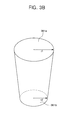
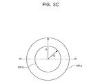
FIG. 3B is a perspective view illustrating a whole shape of each of the
first to third connection holes 261, 262, and 271, FIG. 3C is a plan view of the
connection holes 261, 262, and 271, and FIG. 3D is a cross-sectional view
taken along the line VI-VI of FIG. 3C.
When the first to third connection holes 261, 262, and 271 are formed,
top and bottom surface are circular as shown in FIG. 3C, and the first to third
connection holes 261, 262, and 271 are formed to be tapered so that the top
surface is wider than the bottom surface as shown in FIG. 3D.
This may be expressed as the equation below:
r1 > r2 > 0
where r1 indicates a radius of the top surface of each of the first to third
connection holes 261, 262, and 271, and r2 indicates a radius of the bottom
surface of each of the first to third connection holes 261, 262, and 271.
Corners of the top and bottom surfaces of the first to third connection
holes 261, 262, and 271 are circular, and the bottom surface has a point which
is positioned on the same axis vertically extending from the surface including
the radius center of the top surface, as a radius center. The radius of the top
surface of the connection hole is formed to be larger than that of the bottom
surface, so that a short-circuit failure caused by the edge open of the corners of
the first to third connection holes 261, 262, and 271 may be prevented.
Connection holes which are formed on the inter-insulating layer and the
gate insulating layer for insulating the source and drain regions from the source
and drain electrodes serve as contact holes, and connection holes which are
formed on the passivation layer for insulating the source and drain electrodes
from the lower electrode serve as via holes.
The lower electrode serves as an anode electrode, and the upper
electrode serves as a cathode electrode.
Preferred embodiments of the present invention have been described,
however, the description of the connection holes in the first and second
embodiments may also be applied to the case of forming an opening of the
planarization layer.
According to the present invention as mentioned above, surface corner
portions of contact holes and via holes may be curved so that short-circuit
failures may be reduced to enhance reliability and yield.
Although the present invention has been described with reference to
certain exemplary embodiments thereof, it will be understood by those skilled in
the art that a variety of modifications and variations may be made to the present
invention without departing from the spirit or scope of the present invention
defined in the appended claims, and their equivalents.