EP1566623A1 - Device for measuring the quantity of solid particles in a gas medium - Google Patents
Device for measuring the quantity of solid particles in a gas medium Download PDFInfo
- Publication number
- EP1566623A1 EP1566623A1 EP04425076A EP04425076A EP1566623A1 EP 1566623 A1 EP1566623 A1 EP 1566623A1 EP 04425076 A EP04425076 A EP 04425076A EP 04425076 A EP04425076 A EP 04425076A EP 1566623 A1 EP1566623 A1 EP 1566623A1
- Authority
- EP
- European Patent Office
- Prior art keywords
- cavities
- electrode
- solid particles
- gas medium
- measuring
- Prior art date
- Legal status (The legal status is an assumption and is not a legal conclusion. Google has not performed a legal analysis and makes no representation as to the accuracy of the status listed.)
- Granted
Links
Images

Classifications
-
- G—PHYSICS
- G01—MEASURING; TESTING
- G01N—INVESTIGATING OR ANALYSING MATERIALS BY DETERMINING THEIR CHEMICAL OR PHYSICAL PROPERTIES
- G01N15/00—Investigating characteristics of particles; Investigating permeability, pore-volume or surface-area of porous materials
- G01N15/06—Investigating concentration of particle suspensions
- G01N15/0656—Investigating concentration of particle suspensions using electric, e.g. electrostatic methods or magnetic methods
-
- F—MECHANICAL ENGINEERING; LIGHTING; HEATING; WEAPONS; BLASTING
- F01—MACHINES OR ENGINES IN GENERAL; ENGINE PLANTS IN GENERAL; STEAM ENGINES
- F01N—GAS-FLOW SILENCERS OR EXHAUST APPARATUS FOR MACHINES OR ENGINES IN GENERAL; GAS-FLOW SILENCERS OR EXHAUST APPARATUS FOR INTERNAL-COMBUSTION ENGINES
- F01N2560/00—Exhaust systems with means for detecting or measuring exhaust gas components or characteristics
- F01N2560/05—Exhaust systems with means for detecting or measuring exhaust gas components or characteristics the means being a particulate sensor
Definitions
- the present invention relates to a device for the cumulative measure of the amount of solid particles in a gas medium.
- Devices as referred to above are for instance used for detecting the level of carbon particulate matter in exhaust gases of vehicles with internal combustion engines.
- Known detecting devices include those comprising a flat supporting structure, made of insulating material, to one of whose surfaces at least two electrodes with interdigitized conductive tracks are associated, as well as means designed to measure variations of electrical resistance between said electrodes.
- the supporting structure is arranged inside the exhaust conduit of the vehicle engine, so that part of the particulate matter in exhaust gases can deposit onto said flat surface.
- Particulate matter is basically a conductive compound based on carbon and its particles, depositing onto the flat surface of the device, tend to form conductive bridges between the interdigitized tracks of the electrodes, which results in a progressive decrease of electric resistance at the ends of the latter. Thanks to the variation of electrical resistance with respect to an initial value it is possible to calculate in an integral way the amount of particulate matter in exhaust gases.
- This phenomenon is basically due to the distribution with fractal structure of particulate matter on sensor surface; said structure has a critical interconnection threshold, above which the value of electrical resistance sinks dramatically.
- the present invention aims at carrying out a new device for detecting the amount of solid particles in a gas medium, having in particular a linear, repeatable characteristic curve.
- a device for detecting the amount or concentration of solid particles of nanometric or sub-micrometric size in a gas medium, in particular particulate matter in the exhaust gas of an internal combustion engine comprising:
- detecting devices according to the prior art are basically characterized by a flat structure, defining a surface for particulate matter deposit, on which at least two electrodes are present.
- the detecting device according to the present invention is characterized by the use of a porous matrix, whose cavities are designed to house solid particles of nanometric or sub-micrometric size present in the gas to be analyzed.
- the progressive accumulation of carbon particles in the cavities thus obtained results in a progressive, regular variation of electric resistance.
- the aforesaid matrix is made of porous aluminum oxide (Al 2 O 3 ) obtained by means of an anodization process; said material, hereinafter referred to as alumina, has properties of electrical insulation, is resistant to high temperatures and has a highly regular porous structure.
- alumina porous aluminum oxide
- porous alumina can be ideally schematized as a lattice or reticule of aligned pores, extending from the outer surface to the underlying metal layer.
- Porous alumina can be obtained by means of a particular process of anodization of highly pure aluminum sheets or of aluminum films deposited onto substrates such as glass, quartz, silicon, tungsten, etc.
- Figure 1 shows as a mere example a portion of a porous alumina film, globally referred to with number 1, obtained by means of anodic oxidation of an aluminum layer 2 placed on a convenient substrate S.
- the alumina layer 1 consists of a series of typically hexagonal, directly adjacent cells 3, each having a central straight passage creating a pore 4, basically perpendicular to the surface of the aluminum layer 2.
- the end of each cell 3 on the aluminum layer 2 has a closing portion having a typically hemispheric shape, the whole of said closing portions making up a non-porous part of the film 1, or barrier layer, referred to with number 5.
- the film 1 can be developed with controlled morphology by conveniently choosing the physical, chemical and electro-chemical parameters of the process: in acid electrolytes (such as phosphoric acid, oxalic acid and sulfuric acid) and under suitable process conditions (voltage, current, stirring and temperature), highly regular porous films can be obtained.
- acid electrolytes such as phosphoric acid, oxalic acid and sulfuric acid
- suitable process conditions voltage, current, stirring and temperature
- the size and density of the cells 3 can be varied; for instance the diameter of the pores 4, which is typically of 50-500 nm, can be controlled by chemical treatments.
- the pores of the alumina used in the application here suggested preferably have a diameter of 200-300 nm, so as to enable the entry and therefore the detection of sub-micrometric particulate matter.
- the first step in the manufacturing of the porous alumina film 1 is the deposition of the aluminum layer 2 onto a convenient substrate S, the latter being for instance made of silicon.
- This operation requires a deposit of highly pure materials with thicknesses of one ⁇ m to 50 ⁇ m.
- Preferred techniques for depositing the layer 2 are thermal evaporation via e-beam and sputtering.
- the step including the deposition of the aluminum layer 2 is followed by an anodization step of said layer.
- the anodization process of the layer 2 can be carried out by using different electrolytic solutions depending on the desired size and distance of pores 4.
- the configuration of the electrolytic cell is also important in order to obtain a correct distribution of the shape lines of the electric field with a corresponding uniformity of the anodic process.
- Figure 3 schematically shows the result of the first anodization of the aluminum layer 2; as shown, the alumina film, here referred to with number 1A, obtained through the first anodization of the layer 2, does not have a regular structure.
- the alumina film here referred to with number 1A
- the etching step referred to in ii) is important in order to define on the residual alumina part 1A preferential areas for alumina growth in the second anodization step.
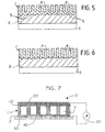
- the structure improves until it becomes highly uniform, as schematically shown in Figure 5, where the alumina film 1 is now regular.
- the barrier layer 5 fully insulates the alumina structure: the reduction of said layer 5 is therefore fundamental so as both to perform consecutive electrodeposition processes, if necessary, requiring an electric contact, and to detect electric quantities, as shall be seen below.
- the aforesaid process involving the removal or reduction of the barrier layer 5 can include two consecutive stages:
- Figure 6 shows the result of the aforesaid process of removal of the barrier layer, as a result of which the pores 4 of the alumina film, now referred to with number 1', open directly also on the underlying aluminum layer 2, on which alumina has been grown, as previously described.
- the following layers are deposited onto the film 1' starting from the side of the structure opposite the aluminum layer 2: a layer of insulating material and a layer of conductive material building an electrode, referred to with numbers 10 and 20, respectively.
- the insulating layer 10 and the electrode 20 can consist of an insulating paste and a conductive paste, respectively, deposited with screen printing techniques or by evaporation onto porous alumina 1'.
- the insulating layer 10 prevents possible short-circuits between the metal layer under alumina and the conductive layer 20.
- the materials constituting the insulating layer 10 and the electrode 20 are deposited so as not to fill up and obstruct the pores 4, so that the latter can act as collectors of solid particles.
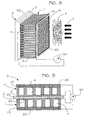
- the insulating layer 10 and the electrode 20 can be arranged as a grid on the porous surface of alumina 1'; Figure 8 only shows the peripheral mesh of said grid, for higher clarity of representation.
- the device D then comprises measuring means 30, known per se, designed to detect the variation of electric resistance, due to the collection of particulate matter in the pores 4, between the electrode 20 and the aluminum layer 2, which constitutes the second electrode of the device D.
- Figure 8 shows schematically the device D in a condition of possible use; to said purpose let us assume that the device D is arranged inside an exhaust tube of a vehicle with internal combustion engine.
- the device D is mounted so that the open end of the pores 4, which overlooks the electrode 20, is opposed to the flow direction normally followed by exhaust gases, as schematically referred to with arrows F.
- gases F which basically consists of sub-micrometric or nanometric particles based on conductive carbon.
- the aforesaid particles are shown schematically by the spots referred to with P in Figure 8; as can be inferred from said figure, the arrangement is such that the flow F causes the entry of particles P into the pores 4 of the alumina film 1' of the device D.
- the method followed for detecting the level of particulate matter includes, in a preliminary phase, the calculation of the resistive component of the impedance of the sensor device, which can be detected between the two electrodes, defined as variable resistance, since it depends on a series of parallel resistances due to the various layers 2, 1', 10, 20 making up the device D.
- Said resistive value is initially in the order of megaohms, since porous alumina - as was said - is a basically insulating material.
- the detection of resistance variation, with the flow F, with respect to an initial value, performed through the measuring means 30, thus allows to carry out an integral "batch” or cumulative integral measuring of the level of particulate matter, according to known techniques (as was mentioned in the introduction to the present description, thanks to the variation of electrical resistance measured with respect to an initial value it is possible to calculate integrally the level of particulate matter in exhaust gases, by means of suitable transfer functions).
- the latter should be "regenerated", by removing the particulate matter P trapped in the pores 4.
- a heater for instance a metal electric resistor, operative to heat the structure of said device and then burn the particulate matter P.
- a resistor for instance shaped like a coil, can be advantageously integrated into a metal support 50 of the device D, so as to be close to the layer 2.
- the resistor 40 is supplied with electric energy, so as to heat the structure of the device up to 630-650°C. i.e. to a temperature causing oxidation and therefore the removal of the particles P collected in the pores 4.
- the device D being a sensor for cumulative measuring of integral type, can be advantageously used for taking measurings in a particulate matter filter present in the exhaust conduit of motor vehicles with internal combustion engines, for instance diesel engines.
- the invention can obviously be used also in other fields than the automotive one, in order to measure the amount or concentration of particles in a generic gas medium.
- Figure 9 shows by way of example a possible execution variant of the invention, according to which the sensor device D comprises two porous structures opposed one to the other with respect to the same support 50 integrating the resistor 40, each structure comprising its own layers 2, 1', 10, 20.
- Said structure which improves the exploitation of a given sensitive area, preferably requires a housing having such fluid-dynamic features as to convey gases carrying particulate matter onto both surfaces of the sensor device D.
- the level of solid particles in the gas medium is calculated on the basis of variations of electric resistance; however, it is obvious for the person skilled in the art that the detections performed by the sensor could be capacitive.
- the electrode referred to above with number 2 should not necessarily be made of aluminum; in such a case the aluminum layer 2 on which alumina 1' has been grown can be removed through known etching techniques, so as to enable the direct contact of said structure with another conductive material acting as electrode of the device.
Landscapes
- Chemical & Material Sciences (AREA)
- Dispersion Chemistry (AREA)
- Physics & Mathematics (AREA)
- Health & Medical Sciences (AREA)
- Life Sciences & Earth Sciences (AREA)
- Analytical Chemistry (AREA)
- Biochemistry (AREA)
- General Health & Medical Sciences (AREA)
- General Physics & Mathematics (AREA)
- Immunology (AREA)
- Pathology (AREA)
- Investigating Or Analyzing Materials By The Use Of Electric Means (AREA)
Abstract
Description
- a structure for the deposit of solid particles present in the gas medium,
- at least a first and a second electrode associated to said structure, and
- means for measuring an electric quantity between the first and second electrode,
- Figure 1 is a schematic perspective view of a portion of a porous film of aluminum oxide (hereinafter referred to as alumina) grown on a metal substrate;
- Figure 2-6 show consecutive steps of a process for making a porous film of aluminum oxide grown on a metal substrate, used in a detecting device according to the invention;
- Figures 7 and 8 are partial, schematic views, a sectioned view and a perspective view respectively, of a device according to the invention;
- Figure 9 is a partial, schematic section of a device carried out in accordance with a possible execution variant of the invention.
- widening of
pores 4, if necessary, performed in the same electrolyte as in previous anodization, without passage of current; - reduction of the
barrier layer 5, performed by passage of very low current in the same electrolyte as in previous anodization; at this stage the typical balance of anodization is not achieved, thus favoring an etching process with respect to an alumina-building process.
Claims (16)
- Device for detecting the amount or concentration of solid particles of nanometric or sub-micrometric size in a gas medium, in particular particulate matter in the exhaust gas of an internal combustion engine, comprising:characterized in that a plurality of cavities (4) is defined in said structure (1'), which act as collectors of solid particles (P) present in the gas medium (F), the structure (1') being arranged so as to enable collection of said particles (P) inside said cavities (4).a structure (1') for the deposit of solid particles (P) present in the gas medium (F),at least a first and a second electrode (2, 20) associated to said structure (1'), andmeans for measuring (30) an electric quantity between the first and second electrode (2, 20),
- Device according to claim 1, characterized in that said structure (1') comprises a porous body (1') made of an electrically insulating material, the pores of said body (1') constituting at least part of said cavities (4).
- Device according to claim 2, characterized in that said porous body (1') is made at least partly of anodized porous alumina.
- Device according to claim 2, characterized in that said porous body (1') is placed between the first and second electrode (2, 20).
- Device according to claim 1, characterized in that a first end of said cavities (4) overlooks said first electrode (2), which acts as closing element for said cavities on said first ends.
- Device according to claim 1, characterized in that a second end of said cavities is open towards said second electrode (20).
- Device according to claim 1, characterized in that an end of said cavities (4) is open so as to receive said particles (P), and is in particular opposed to the direction of a flow of the gas medium (F).
- Device according to claim 4, characterized in that at least one layer of electrically insulating material (10) is placed between said second electrode (20) and said porous body (1').
- Device according to claim 8, characterized in that said second electrode (20) and said insulating layer (10) are shaped like a grid.
- Device according to claim 1, characterized in that said measuring means (30) comprise means for measuring at least one between electric resistance and capacity.
- Device according to claim 1, characterized in that said measuring means (30) are operative to detect a variation in the value of the measured quantity with respect to an initial or reference value, and to estimate in an integral way, as a function of said variation, the amount or concentration of solid particles (P) in the gas medium (F).
- Device according to claim 1, characterized in that it comprises regeneration means (40), which can be activated in order to remove from said cavities (4) the solid particles (P) therein collected.
- Device according to claim 11, characterized in that said regeneration means comprise heating means (40), which can heat said structure up to a temperature causing oxidation or anyhow the removal of the solid particles (P) collected in said cavities (4).
- Device according to claim 5, characterized in that said first electrode (2) is at least partly made of aluminum.
- Device according to one or more of the preceding claims, characterized in that it is installed inside an exhaust conduit of an internal combustion engine.
- Use of the device according to one or more of the preceding claims for detecting the concentration of particulate matter in exhaust gases of an internal combustion engine of a motor vehicle, in particular a diesel engine.
Priority Applications (2)
| Application Number | Priority Date | Filing Date | Title |
|---|---|---|---|
| EP04425076.9A EP1566623B1 (en) | 2004-02-06 | 2004-02-06 | Device for measuring the quantity of solid particles in a gas medium |
| US11/040,105 US7350397B2 (en) | 2004-02-06 | 2005-01-24 | Device for measuring the quantity of solid particles in a gas medium |
Applications Claiming Priority (1)
| Application Number | Priority Date | Filing Date | Title |
|---|---|---|---|
| EP04425076.9A EP1566623B1 (en) | 2004-02-06 | 2004-02-06 | Device for measuring the quantity of solid particles in a gas medium |
Publications (2)
| Publication Number | Publication Date |
|---|---|
| EP1566623A1 true EP1566623A1 (en) | 2005-08-24 |
| EP1566623B1 EP1566623B1 (en) | 2013-12-18 |
Family
ID=34707423
Family Applications (1)
| Application Number | Title | Priority Date | Filing Date |
|---|---|---|---|
| EP04425076.9A Expired - Lifetime EP1566623B1 (en) | 2004-02-06 | 2004-02-06 | Device for measuring the quantity of solid particles in a gas medium |
Country Status (2)
| Country | Link |
|---|---|
| US (1) | US7350397B2 (en) |
| EP (1) | EP1566623B1 (en) |
Cited By (2)
| Publication number | Priority date | Publication date | Assignee | Title |
|---|---|---|---|---|
| WO2011154802A1 (en) * | 2010-06-10 | 2011-12-15 | Toyota Jidosha Kabushiki Kaisha | Particulate matter amount detection system |
| EP2128597A4 (en) * | 2007-03-27 | 2014-05-28 | Ngk Insulators Ltd | Fine particle sensor |
Families Citing this family (9)
| Publication number | Priority date | Publication date | Assignee | Title |
|---|---|---|---|---|
| US7810314B2 (en) * | 2007-06-12 | 2010-10-12 | Ford Global Technologies, Llc | Approach for controlling particulate matter in an engine |
| DE102010029575A1 (en) * | 2010-06-01 | 2011-12-01 | Robert Bosch Gmbh | Method and particle sensor for detecting particles in an exhaust gas stream |
| KR101305198B1 (en) | 2011-12-09 | 2013-09-26 | 현대자동차주식회사 | Particulate matters sensor unit |
| KR101972887B1 (en) * | 2014-12-23 | 2019-04-26 | 헤래우스 센서 테크놀로지 게엠베하 | Sensors for detecting conductive and / or polarized particles and methods of controlling such sensors |
| JP2016153737A (en) * | 2015-02-20 | 2016-08-25 | いすゞ自動車株式会社 | Sensor |
| JP2016153610A (en) * | 2015-02-20 | 2016-08-25 | いすゞ自動車株式会社 | Exhaust emission control device |
| CN105717001A (en) * | 2016-01-05 | 2016-06-29 | 南京大学(苏州)高新技术研究院 | Characterization method of atmospheric solid particulate matter [PM 2.5] indexes measured according to conductivity |
| CN105758768A (en) * | 2016-01-07 | 2016-07-13 | 南京大学(苏州)高新技术研究院 | Characterization method of electroconductive particulate matter (PMd) index measured according to electroconductivity |
| JP6705269B2 (en) * | 2016-04-14 | 2020-06-03 | いすゞ自動車株式会社 | Sensor |
Citations (2)
| Publication number | Priority date | Publication date | Assignee | Title |
|---|---|---|---|---|
| US4979364A (en) * | 1988-03-11 | 1990-12-25 | Fleck Carl M | Diesel fuel exhaust gas filter |
| US20020118027A1 (en) * | 2000-10-24 | 2002-08-29 | Dmitri Routkevitch | Nanostructured ceramic platform for micromachined devices and device arrays |
Family Cites Families (13)
| Publication number | Priority date | Publication date | Assignee | Title |
|---|---|---|---|---|
| JPS60174940A (en) * | 1984-02-21 | 1985-09-09 | Fuigaro Giken Kk | Detection of trace substance in gas |
| US5008628A (en) * | 1989-06-05 | 1991-04-16 | Wahlco, Inc. | Measurement of electrical resistivity of particulate entrained in a gas stream |
| US5247827A (en) * | 1992-04-14 | 1993-09-28 | Bell Communications Research, Inc. | Resistive measurement of airborne contaminants |
| US5581091A (en) * | 1994-12-01 | 1996-12-03 | Moskovits; Martin | Nanoelectric devices |
| US5756879A (en) * | 1996-07-25 | 1998-05-26 | Hughes Electronics | Volatile organic compound sensors |
| US6231744B1 (en) * | 1997-04-24 | 2001-05-15 | Massachusetts Institute Of Technology | Process for fabricating an array of nanowires |
| US6638654B2 (en) * | 1999-02-01 | 2003-10-28 | The Regents Of The University Of California | MEMS-based thin-film fuel cells |
| US6350623B1 (en) * | 1999-10-29 | 2002-02-26 | California Institute Of Technology | Method of forming intermediate structures in porous substrates in which electrical and optical microdevices are fabricated and intermediate structures formed by the same |
| DE10020539A1 (en) * | 2000-04-27 | 2001-11-08 | Heraeus Electro Nite Int | Measuring arrangement and method for determining soot concentrations |
| DE10130163B4 (en) * | 2000-11-21 | 2012-01-12 | Siemens Ag | Arrangement for reducing carbonaceous particulate emissions from diesel engines |
| US6709929B2 (en) * | 2001-06-25 | 2004-03-23 | North Carolina State University | Methods of forming nano-scale electronic and optoelectronic devices using non-photolithographically defined nano-channel templates |
| WO2005001021A2 (en) * | 2002-06-06 | 2005-01-06 | California Institute Of Technology | Nanocarpets for trapping particulates, bacteria and spores |
| US8044584B2 (en) * | 2004-11-08 | 2011-10-25 | Samsung Mobile Display Co., Ltd. | Organic electroluminescent device and method for manufacturing the same |
-
2004
- 2004-02-06 EP EP04425076.9A patent/EP1566623B1/en not_active Expired - Lifetime
-
2005
- 2005-01-24 US US11/040,105 patent/US7350397B2/en not_active Expired - Fee Related
Patent Citations (2)
| Publication number | Priority date | Publication date | Assignee | Title |
|---|---|---|---|---|
| US4979364A (en) * | 1988-03-11 | 1990-12-25 | Fleck Carl M | Diesel fuel exhaust gas filter |
| US20020118027A1 (en) * | 2000-10-24 | 2002-08-29 | Dmitri Routkevitch | Nanostructured ceramic platform for micromachined devices and device arrays |
Non-Patent Citations (1)
| Title |
|---|
| ROUTKEVITCH ET AL: "Nonlithographic Nano-Wire Arrays: Fabrication, Physics, and Device Applications", IEEE TRANSACTIONS ON ELECTRON DEVICES, vol. 43, no. 10, October 1996 (1996-10-01), pages 1646 - 1658, XP002277875 * |
Cited By (3)
| Publication number | Priority date | Publication date | Assignee | Title |
|---|---|---|---|---|
| EP2128597A4 (en) * | 2007-03-27 | 2014-05-28 | Ngk Insulators Ltd | Fine particle sensor |
| WO2011154802A1 (en) * | 2010-06-10 | 2011-12-15 | Toyota Jidosha Kabushiki Kaisha | Particulate matter amount detection system |
| US9354154B2 (en) | 2010-06-10 | 2016-05-31 | Toyota Jidosha Kabushiki Kaisha | Particulate matter amount detection system |
Also Published As
| Publication number | Publication date |
|---|---|
| EP1566623B1 (en) | 2013-12-18 |
| US20050180888A1 (en) | 2005-08-18 |
| US7350397B2 (en) | 2008-04-01 |
Similar Documents
| Publication | Publication Date | Title |
|---|---|---|
| US7350397B2 (en) | Device for measuring the quantity of solid particles in a gas medium | |
| JP4691096B2 (en) | Method for the control of soot deposition on a sensor | |
| JP2009085959A (en) | Sensor element for detecting particles in gas and method for manufacturing the sensor element | |
| Lasia | Modeling of impedance of porous electrodes | |
| US20170363530A1 (en) | Sensor for detecting electrically conductive and/or polarizable particles, sensor system, method for operating a sensor, method for producing a sensor of this type and use of a sensor of this type | |
| US20010051108A1 (en) | Sensor and method for determining soot concentrations | |
| EP2128597A1 (en) | Fine particle sensor | |
| DE102007021913A1 (en) | Method and sensor for detecting particles in a gas stream and their use | |
| EP2369331B1 (en) | Gas sensor | |
| Bartscherer et al. | Improvement of the sensitivity of a conductometric soot sensor by adding a conductive cover layer | |
| JP4742133B2 (en) | Particulate matter detection device and particulate matter detection method | |
| CN102183558B (en) | Graded porous nano alumina/gold composite film electrode and preparation method thereof | |
| KR20100105023A (en) | Gas sensor using metal oxide nano rod and manufacturing method thereof | |
| CN101109725A (en) | Surface-sensitive capacitive gas sensor and manufacturing method thereof | |
| CN110608980A (en) | Exhaust particulate matter sensor | |
| JP2010261782A (en) | Soot detector and soot detection method | |
| DE102008007664A1 (en) | Ceramic heating element for use in electrochemical gas sensor that detects soot particle in exhaust gas of e.g. internal combustion engine, has electric resistor elements arranged parallel to each other in ceramic layer plane | |
| US10126224B2 (en) | Particle sensor and method for manufacturing a particle sensor | |
| KR102687799B1 (en) | Method for determining adhesion of layers of a ceramic sensor element for detecting at least one property of a measuring gas in a measuring gas chamber | |
| JP2603373B2 (en) | Electrochemical element | |
| CN115150977A (en) | Method for estimating heat generation distribution of honeycomb structure, method for manufacturing honeycomb structure, and method for manufacturing electrically heated carrier | |
| CN1294414C (en) | Method for producing gas sensor using oriented carbon nano tube layer as gas sensitive layer | |
| JP3594726B2 (en) | Method for forming porous film on ceramic body | |
| WO2006077198A1 (en) | Measuring arrangement and method for determining the concentration of particles in gas mixtures | |
| DE102006032549A1 (en) | Sensor element for determining gas component or particles, comprises carrier body with through hole , where sensitive area of sensor element is arranged as ceramic membrane in through hole and has measuring electrodes |
Legal Events
| Date | Code | Title | Description |
|---|---|---|---|
| PUAI | Public reference made under article 153(3) epc to a published international application that has entered the european phase |
Free format text: ORIGINAL CODE: 0009012 |
|
| 17P | Request for examination filed |
Effective date: 20041129 |
|
| AK | Designated contracting states |
Kind code of ref document: A1 Designated state(s): AT BE BG CH CY CZ DE DK EE ES FI FR GB GR HU IE IT LI LU MC NL PT RO SE SI SK TR |
|
| AX | Request for extension of the european patent |
Extension state: AL LT LV MK |
|
| AKX | Designation fees paid |
Designated state(s): AT BE BG CH CY CZ DE DK EE ES FI FR GB GR HU IE IT LI LU MC NL PT RO SE SI SK TR |
|
| 17Q | First examination report despatched |
Effective date: 20061128 |
|
| GRAP | Despatch of communication of intention to grant a patent |
Free format text: ORIGINAL CODE: EPIDOSNIGR1 |
|
| RIC1 | Information provided on ipc code assigned before grant |
Ipc: G01N 15/06 20060101AFI20130626BHEP Ipc: F01N 11/00 20060101ALI20130626BHEP |
|
| INTG | Intention to grant announced |
Effective date: 20130716 |
|
| GRAS | Grant fee paid |
Free format text: ORIGINAL CODE: EPIDOSNIGR3 |
|
| GRAA | (expected) grant |
Free format text: ORIGINAL CODE: 0009210 |
|
| AK | Designated contracting states |
Kind code of ref document: B1 Designated state(s): AT BE BG CH CY CZ DE DK EE ES FI FR GB GR HU IE IT LI LU MC NL PT RO SE SI SK TR |
|
| REG | Reference to a national code |
Ref country code: GB Ref legal event code: FG4D |
|
| REG | Reference to a national code |
Ref country code: CH Ref legal event code: EP |
|
| REG | Reference to a national code |
Ref country code: AT Ref legal event code: REF Ref document number: 645830 Country of ref document: AT Kind code of ref document: T Effective date: 20140115 |
|
| REG | Reference to a national code |
Ref country code: IE Ref legal event code: FG4D |
|
| REG | Reference to a national code |
Ref country code: DE Ref legal event code: R096 Ref document number: 602004044009 Country of ref document: DE Effective date: 20140213 |
|
| REG | Reference to a national code |
Ref country code: NL Ref legal event code: VDEP Effective date: 20131218 |
|
| PG25 | Lapsed in a contracting state [announced via postgrant information from national office to epo] |
Ref country code: SE Free format text: LAPSE BECAUSE OF FAILURE TO SUBMIT A TRANSLATION OF THE DESCRIPTION OR TO PAY THE FEE WITHIN THE PRESCRIBED TIME-LIMIT Effective date: 20131218 Ref country code: FI Free format text: LAPSE BECAUSE OF FAILURE TO SUBMIT A TRANSLATION OF THE DESCRIPTION OR TO PAY THE FEE WITHIN THE PRESCRIBED TIME-LIMIT Effective date: 20131218 |
|
| PGFP | Annual fee paid to national office [announced via postgrant information from national office to epo] |
Ref country code: DE Payment date: 20140129 Year of fee payment: 11 |
|
| REG | Reference to a national code |
Ref country code: AT Ref legal event code: MK05 Ref document number: 645830 Country of ref document: AT Kind code of ref document: T Effective date: 20131218 |
|
| PGFP | Annual fee paid to national office [announced via postgrant information from national office to epo] |
Ref country code: FR Payment date: 20140211 Year of fee payment: 11 |
|
| PG25 | Lapsed in a contracting state [announced via postgrant information from national office to epo] |
Ref country code: EE Free format text: LAPSE BECAUSE OF FAILURE TO SUBMIT A TRANSLATION OF THE DESCRIPTION OR TO PAY THE FEE WITHIN THE PRESCRIBED TIME-LIMIT Effective date: 20131218 Ref country code: BE Free format text: LAPSE BECAUSE OF FAILURE TO SUBMIT A TRANSLATION OF THE DESCRIPTION OR TO PAY THE FEE WITHIN THE PRESCRIBED TIME-LIMIT Effective date: 20131218 |
|
| PG25 | Lapsed in a contracting state [announced via postgrant information from national office to epo] |
Ref country code: RO Free format text: LAPSE BECAUSE OF FAILURE TO SUBMIT A TRANSLATION OF THE DESCRIPTION OR TO PAY THE FEE WITHIN THE PRESCRIBED TIME-LIMIT Effective date: 20131218 Ref country code: PT Free format text: LAPSE BECAUSE OF FAILURE TO SUBMIT A TRANSLATION OF THE DESCRIPTION OR TO PAY THE FEE WITHIN THE PRESCRIBED TIME-LIMIT Effective date: 20140418 Ref country code: CY Free format text: LAPSE BECAUSE OF FAILURE TO SUBMIT A TRANSLATION OF THE DESCRIPTION OR TO PAY THE FEE WITHIN THE PRESCRIBED TIME-LIMIT Effective date: 20131218 Ref country code: ES Free format text: LAPSE BECAUSE OF FAILURE TO SUBMIT A TRANSLATION OF THE DESCRIPTION OR TO PAY THE FEE WITHIN THE PRESCRIBED TIME-LIMIT Effective date: 20131218 Ref country code: SK Free format text: LAPSE BECAUSE OF FAILURE TO SUBMIT A TRANSLATION OF THE DESCRIPTION OR TO PAY THE FEE WITHIN THE PRESCRIBED TIME-LIMIT Effective date: 20131218 Ref country code: CZ Free format text: LAPSE BECAUSE OF FAILURE TO SUBMIT A TRANSLATION OF THE DESCRIPTION OR TO PAY THE FEE WITHIN THE PRESCRIBED TIME-LIMIT Effective date: 20131218 Ref country code: NL Free format text: LAPSE BECAUSE OF FAILURE TO SUBMIT A TRANSLATION OF THE DESCRIPTION OR TO PAY THE FEE WITHIN THE PRESCRIBED TIME-LIMIT Effective date: 20131218 Ref country code: AT Free format text: LAPSE BECAUSE OF FAILURE TO SUBMIT A TRANSLATION OF THE DESCRIPTION OR TO PAY THE FEE WITHIN THE PRESCRIBED TIME-LIMIT Effective date: 20131218 |
|
| REG | Reference to a national code |
Ref country code: DE Ref legal event code: R097 Ref document number: 602004044009 Country of ref document: DE |
|
| PG25 | Lapsed in a contracting state [announced via postgrant information from national office to epo] |
Ref country code: MC Free format text: LAPSE BECAUSE OF FAILURE TO SUBMIT A TRANSLATION OF THE DESCRIPTION OR TO PAY THE FEE WITHIN THE PRESCRIBED TIME-LIMIT Effective date: 20131218 Ref country code: LU Free format text: LAPSE BECAUSE OF FAILURE TO SUBMIT A TRANSLATION OF THE DESCRIPTION OR TO PAY THE FEE WITHIN THE PRESCRIBED TIME-LIMIT Effective date: 20140206 |
|
| REG | Reference to a national code |
Ref country code: CH Ref legal event code: PL |
|
| PLBE | No opposition filed within time limit |
Free format text: ORIGINAL CODE: 0009261 |
|
| STAA | Information on the status of an ep patent application or granted ep patent |
Free format text: STATUS: NO OPPOSITION FILED WITHIN TIME LIMIT |
|
| PG25 | Lapsed in a contracting state [announced via postgrant information from national office to epo] |
Ref country code: DK Free format text: LAPSE BECAUSE OF FAILURE TO SUBMIT A TRANSLATION OF THE DESCRIPTION OR TO PAY THE FEE WITHIN THE PRESCRIBED TIME-LIMIT Effective date: 20131218 Ref country code: CH Free format text: LAPSE BECAUSE OF NON-PAYMENT OF DUE FEES Effective date: 20140228 Ref country code: LI Free format text: LAPSE BECAUSE OF NON-PAYMENT OF DUE FEES Effective date: 20140228 |
|
| 26N | No opposition filed |
Effective date: 20140919 |
|
| GBPC | Gb: european patent ceased through non-payment of renewal fee |
Effective date: 20140318 |
|
| REG | Reference to a national code |
Ref country code: IE Ref legal event code: MM4A |
|
| REG | Reference to a national code |
Ref country code: DE Ref legal event code: R097 Ref document number: 602004044009 Country of ref document: DE Effective date: 20140919 |
|
| PG25 | Lapsed in a contracting state [announced via postgrant information from national office to epo] |
Ref country code: GB Free format text: LAPSE BECAUSE OF NON-PAYMENT OF DUE FEES Effective date: 20140318 Ref country code: IE Free format text: LAPSE BECAUSE OF NON-PAYMENT OF DUE FEES Effective date: 20140206 |
|
| PGFP | Annual fee paid to national office [announced via postgrant information from national office to epo] |
Ref country code: IT Payment date: 20141022 Year of fee payment: 12 |
|
| PG25 | Lapsed in a contracting state [announced via postgrant information from national office to epo] |
Ref country code: SI Free format text: LAPSE BECAUSE OF FAILURE TO SUBMIT A TRANSLATION OF THE DESCRIPTION OR TO PAY THE FEE WITHIN THE PRESCRIBED TIME-LIMIT Effective date: 20131218 |
|
| REG | Reference to a national code |
Ref country code: DE Ref legal event code: R119 Ref document number: 602004044009 Country of ref document: DE |
|
| REG | Reference to a national code |
Ref country code: FR Ref legal event code: ST Effective date: 20151030 |
|
| PG25 | Lapsed in a contracting state [announced via postgrant information from national office to epo] |
Ref country code: DE Free format text: LAPSE BECAUSE OF NON-PAYMENT OF DUE FEES Effective date: 20150901 |
|
| PG25 | Lapsed in a contracting state [announced via postgrant information from national office to epo] |
Ref country code: FR Free format text: LAPSE BECAUSE OF NON-PAYMENT OF DUE FEES Effective date: 20150302 |
|
| PG25 | Lapsed in a contracting state [announced via postgrant information from national office to epo] |
Ref country code: BG Free format text: LAPSE BECAUSE OF FAILURE TO SUBMIT A TRANSLATION OF THE DESCRIPTION OR TO PAY THE FEE WITHIN THE PRESCRIBED TIME-LIMIT Effective date: 20131218 |
|
| PG25 | Lapsed in a contracting state [announced via postgrant information from national office to epo] |
Ref country code: GR Free format text: LAPSE BECAUSE OF FAILURE TO SUBMIT A TRANSLATION OF THE DESCRIPTION OR TO PAY THE FEE WITHIN THE PRESCRIBED TIME-LIMIT Effective date: 20140319 |
|
| PG25 | Lapsed in a contracting state [announced via postgrant information from national office to epo] |
Ref country code: HU Free format text: LAPSE BECAUSE OF FAILURE TO SUBMIT A TRANSLATION OF THE DESCRIPTION OR TO PAY THE FEE WITHIN THE PRESCRIBED TIME-LIMIT; INVALID AB INITIO Effective date: 20040206 Ref country code: TR Free format text: LAPSE BECAUSE OF FAILURE TO SUBMIT A TRANSLATION OF THE DESCRIPTION OR TO PAY THE FEE WITHIN THE PRESCRIBED TIME-LIMIT Effective date: 20131218 |
|
| PG25 | Lapsed in a contracting state [announced via postgrant information from national office to epo] |
Ref country code: IT Free format text: LAPSE BECAUSE OF NON-PAYMENT OF DUE FEES Effective date: 20160206 |