EP1565786B1 - Prozess zur herstellung von dicken optischen nichtlineargittern - Google Patents
Prozess zur herstellung von dicken optischen nichtlineargittern Download PDFInfo
- Publication number
- EP1565786B1 EP1565786B1 EP03789450.8A EP03789450A EP1565786B1 EP 1565786 B1 EP1565786 B1 EP 1565786B1 EP 03789450 A EP03789450 A EP 03789450A EP 1565786 B1 EP1565786 B1 EP 1565786B1
- Authority
- EP
- European Patent Office
- Prior art keywords
- face
- initial
- optical grating
- grating
- linear optical
- Prior art date
- Legal status (The legal status is an assumption and is not a legal conclusion. Google has not performed a legal analysis and makes no representation as to the accuracy of the status listed.)
- Expired - Lifetime
Links
- 230000003287 optical effect Effects 0.000 title claims description 59
- 238000000034 method Methods 0.000 title claims description 33
- 230000009021 linear effect Effects 0.000 title claims description 29
- 239000000758 substrate Substances 0.000 claims description 27
- 239000000463 material Substances 0.000 claims description 17
- 238000002248 hydride vapour-phase epitaxy Methods 0.000 claims description 12
- 238000004519 manufacturing process Methods 0.000 claims description 12
- 239000013078 crystal Substances 0.000 claims description 11
- 238000001451 molecular beam epitaxy Methods 0.000 claims description 9
- 238000005498 polishing Methods 0.000 claims description 9
- 238000000151 deposition Methods 0.000 claims description 6
- 239000002178 crystalline material Substances 0.000 claims description 5
- 238000004140 cleaning Methods 0.000 claims description 2
- 239000002243 precursor Substances 0.000 claims description 2
- 238000002488 metal-organic chemical vapour deposition Methods 0.000 claims 2
- JBRZTFJDHDCESZ-UHFFFAOYSA-N AsGa Chemical compound [As]#[Ga] JBRZTFJDHDCESZ-UHFFFAOYSA-N 0.000 description 12
- 229910017214 AsGa Inorganic materials 0.000 description 6
- 239000012071 phase Substances 0.000 description 5
- 229910001218 Gallium arsenide Inorganic materials 0.000 description 4
- 230000008021 deposition Effects 0.000 description 3
- 238000009499 grossing Methods 0.000 description 3
- 125000002524 organometallic group Chemical group 0.000 description 3
- 230000010287 polarization Effects 0.000 description 3
- 238000002360 preparation method Methods 0.000 description 3
- 239000004065 semiconductor Substances 0.000 description 3
- SKJCKYVIQGBWTN-UHFFFAOYSA-N (4-hydroxyphenyl) methanesulfonate Chemical compound CS(=O)(=O)OC1=CC=C(O)C=C1 SKJCKYVIQGBWTN-UHFFFAOYSA-N 0.000 description 2
- PFNQVRZLDWYSCW-UHFFFAOYSA-N (fluoren-9-ylideneamino) n-naphthalen-1-ylcarbamate Chemical compound C12=CC=CC=C2C2=CC=CC=C2C1=NOC(=O)NC1=CC=CC2=CC=CC=C12 PFNQVRZLDWYSCW-UHFFFAOYSA-N 0.000 description 2
- MARUHZGHZWCEQU-UHFFFAOYSA-N 5-phenyl-2h-tetrazole Chemical compound C1=CC=CC=C1C1=NNN=N1 MARUHZGHZWCEQU-UHFFFAOYSA-N 0.000 description 2
- MDPILPRLPQYEEN-UHFFFAOYSA-N aluminium arsenide Chemical compound [As]#[Al] MDPILPRLPQYEEN-UHFFFAOYSA-N 0.000 description 2
- 238000005229 chemical vapour deposition Methods 0.000 description 2
- 230000005684 electric field Effects 0.000 description 2
- 238000000407 epitaxy Methods 0.000 description 2
- 230000003993 interaction Effects 0.000 description 2
- GQYHUHYESMUTHG-UHFFFAOYSA-N lithium niobate Chemical compound [Li+].[O-][Nb](=O)=O GQYHUHYESMUTHG-UHFFFAOYSA-N 0.000 description 2
- 238000004377 microelectronic Methods 0.000 description 2
- 230000002787 reinforcement Effects 0.000 description 2
- 239000011669 selenium Substances 0.000 description 2
- 239000000126 substance Substances 0.000 description 2
- 235000012431 wafers Nutrition 0.000 description 2
- 229910000980 Aluminium gallium arsenide Inorganic materials 0.000 description 1
- GYHNNYVSQQEPJS-UHFFFAOYSA-N Gallium Chemical compound [Ga] GYHNNYVSQQEPJS-UHFFFAOYSA-N 0.000 description 1
- JMASRVWKEDWRBT-UHFFFAOYSA-N Gallium nitride Chemical compound [Ga]#N JMASRVWKEDWRBT-UHFFFAOYSA-N 0.000 description 1
- GPXJNWSHGFTCBW-UHFFFAOYSA-N Indium phosphide Chemical compound [In]#P GPXJNWSHGFTCBW-UHFFFAOYSA-N 0.000 description 1
- BUGBHKTXTAQXES-UHFFFAOYSA-N Selenium Chemical compound [Se] BUGBHKTXTAQXES-UHFFFAOYSA-N 0.000 description 1
- 238000005299 abrasion Methods 0.000 description 1
- 238000006243 chemical reaction Methods 0.000 description 1
- 238000010411 cooking Methods 0.000 description 1
- 238000005520 cutting process Methods 0.000 description 1
- 230000007547 defect Effects 0.000 description 1
- 239000006185 dispersion Substances 0.000 description 1
- 230000009977 dual effect Effects 0.000 description 1
- 229910052733 gallium Inorganic materials 0.000 description 1
- 230000009643 growth defect Effects 0.000 description 1
- WPYVAWXEWQSOGY-UHFFFAOYSA-N indium antimonide Chemical compound [Sb]#[In] WPYVAWXEWQSOGY-UHFFFAOYSA-N 0.000 description 1
- RPQDHPTXJYYUPQ-UHFFFAOYSA-N indium arsenide Chemical compound [In]#[As] RPQDHPTXJYYUPQ-UHFFFAOYSA-N 0.000 description 1
- 238000012986 modification Methods 0.000 description 1
- 230000004048 modification Effects 0.000 description 1
- 230000009022 nonlinear effect Effects 0.000 description 1
- 230000000737 periodic effect Effects 0.000 description 1
- 230000000704 physical effect Effects 0.000 description 1
- 230000008569 process Effects 0.000 description 1
- 230000001902 propagating effect Effects 0.000 description 1
- 229910052711 selenium Inorganic materials 0.000 description 1
- 230000003595 spectral effect Effects 0.000 description 1
- 229910052714 tellurium Inorganic materials 0.000 description 1
- PORWMNRCUJJQNO-UHFFFAOYSA-N tellurium atom Chemical compound [Te] PORWMNRCUJJQNO-UHFFFAOYSA-N 0.000 description 1
- 238000000927 vapour-phase epitaxy Methods 0.000 description 1
Images




Classifications
-
- G—PHYSICS
- G02—OPTICS
- G02F—OPTICAL DEVICES OR ARRANGEMENTS FOR THE CONTROL OF LIGHT BY MODIFICATION OF THE OPTICAL PROPERTIES OF THE MEDIA OF THE ELEMENTS INVOLVED THEREIN; NON-LINEAR OPTICS; FREQUENCY-CHANGING OF LIGHT; OPTICAL LOGIC ELEMENTS; OPTICAL ANALOGUE/DIGITAL CONVERTERS
- G02F1/00—Devices or arrangements for the control of the intensity, colour, phase, polarisation or direction of light arriving from an independent light source, e.g. switching, gating or modulating; Non-linear optics
- G02F1/35—Non-linear optics
- G02F1/37—Non-linear optics for second-harmonic generation
- G02F1/377—Non-linear optics for second-harmonic generation in an optical waveguide structure
- G02F1/3775—Non-linear optics for second-harmonic generation in an optical waveguide structure with a periodic structure, e.g. domain inversion, for quasi-phase-matching [QPM]
-
- B—PERFORMING OPERATIONS; TRANSPORTING
- B82—NANOTECHNOLOGY
- B82Y—SPECIFIC USES OR APPLICATIONS OF NANOSTRUCTURES; MEASUREMENT OR ANALYSIS OF NANOSTRUCTURES; MANUFACTURE OR TREATMENT OF NANOSTRUCTURES
- B82Y20/00—Nanooptics, e.g. quantum optics or photonic crystals
-
- G—PHYSICS
- G02—OPTICS
- G02F—OPTICAL DEVICES OR ARRANGEMENTS FOR THE CONTROL OF LIGHT BY MODIFICATION OF THE OPTICAL PROPERTIES OF THE MEDIA OF THE ELEMENTS INVOLVED THEREIN; NON-LINEAR OPTICS; FREQUENCY-CHANGING OF LIGHT; OPTICAL LOGIC ELEMENTS; OPTICAL ANALOGUE/DIGITAL CONVERTERS
- G02F1/00—Devices or arrangements for the control of the intensity, colour, phase, polarisation or direction of light arriving from an independent light source, e.g. switching, gating or modulating; Non-linear optics
- G02F1/35—Non-linear optics
- G02F1/3501—Constructional details or arrangements of non-linear optical devices, e.g. shape of non-linear crystals
-
- G—PHYSICS
- G02—OPTICS
- G02F—OPTICAL DEVICES OR ARRANGEMENTS FOR THE CONTROL OF LIGHT BY MODIFICATION OF THE OPTICAL PROPERTIES OF THE MEDIA OF THE ELEMENTS INVOLVED THEREIN; NON-LINEAR OPTICS; FREQUENCY-CHANGING OF LIGHT; OPTICAL LOGIC ELEMENTS; OPTICAL ANALOGUE/DIGITAL CONVERTERS
- G02F1/00—Devices or arrangements for the control of the intensity, colour, phase, polarisation or direction of light arriving from an independent light source, e.g. switching, gating or modulating; Non-linear optics
- G02F1/35—Non-linear optics
- G02F1/353—Frequency conversion, i.e. wherein a light beam is generated with frequency components different from those of the incident light beams
- G02F1/3544—Particular phase matching techniques
- G02F1/3548—Quasi phase matching [QPM], e.g. using a periodic domain inverted structure
-
- G—PHYSICS
- G02—OPTICS
- G02F—OPTICAL DEVICES OR ARRANGEMENTS FOR THE CONTROL OF LIGHT BY MODIFICATION OF THE OPTICAL PROPERTIES OF THE MEDIA OF THE ELEMENTS INVOLVED THEREIN; NON-LINEAR OPTICS; FREQUENCY-CHANGING OF LIGHT; OPTICAL LOGIC ELEMENTS; OPTICAL ANALOGUE/DIGITAL CONVERTERS
- G02F1/00—Devices or arrangements for the control of the intensity, colour, phase, polarisation or direction of light arriving from an independent light source, e.g. switching, gating or modulating; Non-linear optics
- G02F1/35—Non-linear optics
- G02F1/355—Non-linear optics characterised by the materials used
- G02F1/3556—Semiconductor materials, e.g. quantum wells
-
- G—PHYSICS
- G02—OPTICS
- G02F—OPTICAL DEVICES OR ARRANGEMENTS FOR THE CONTROL OF LIGHT BY MODIFICATION OF THE OPTICAL PROPERTIES OF THE MEDIA OF THE ELEMENTS INVOLVED THEREIN; NON-LINEAR OPTICS; FREQUENCY-CHANGING OF LIGHT; OPTICAL LOGIC ELEMENTS; OPTICAL ANALOGUE/DIGITAL CONVERTERS
- G02F1/00—Devices or arrangements for the control of the intensity, colour, phase, polarisation or direction of light arriving from an independent light source, e.g. switching, gating or modulating; Non-linear optics
- G02F1/35—Non-linear optics
- G02F1/355—Non-linear optics characterised by the materials used
- G02F1/3558—Poled materials, e.g. with periodic poling; Fabrication of domain inverted structures, e.g. for quasi-phase-matching [QPM]
Definitions
- the field of the invention is that of nonlinear optical gratings.
- the interaction of light with an optically nonlinear material modifies the optical properties. This generates one or more light waves whose frequencies, phases or polarizations are different from that of the incident light.
- the applications are numerous. These include doublers and optical frequency mixers or optical parametric amplifiers and oscillators used in the fields of power lasers or high-speed telecommunications.
- the nonlinear optical effect depends on the susceptibility tensor of the material connecting the induced polarization of the generated wave to the electric field of the incident wave.
- this matrix-form tensor comprises 27 components called non-linear coefficients and noted d.
- the quadratic or order 2 nonlinear processes that are most frequently used require the phase agreement between the incident wave called pump wave and the wave or waves generated called harmonic waves during propagation in the non-linear medium.
- linear The dispersion of the optical indices between the pump wave and the harmonic waves makes it possible in practice to satisfy this condition only in a limited number of birefringent materials. Unfortunately, these materials do not necessarily have the best non-linear coefficients, large wavelength ranges, sufficient ranges of use and focus of the beams.
- nonlinear optical gratings composed of structures based on nonlinear optical crystals makes it possible, under certain conditions, to overcome some of these limitations.
- the technique of the Near Phase Agreement (QAP) is used. This consists in making local modifications of the non-linear properties of a nonlinear crystal so that the phase mismatch between the waves accumulated during the propagation is periodically compensated ( JA Armstrong, N. Bloembergen, J. Ducuing and PS Pershan, "Interactions between light waves in a nonlinear dielectric ", Physical Review, Vol. 127, No. 6, pp. 1918-1939, 1962 ).
- ferroelectric materials such as lithium niobate
- invert the sign of the dielectric polarization of domains of a few microns wide, throughout the depth of the substrates by applying an electric field along the crystallographic axis Z of this material.
- d be the nonlinear coefficient involved
- a beam propagating perpendicular to the crystallographic axis Z sees a modulation of the susceptibility of the type + d / -d / + d / -d / + d / ..., which is propitious at QAP.
- GaAs gallium arsenide
- the epitaxial deposition methods make it possible to fabricate periodically inverted crystalline AsGa structures with fewer constraints than the previous technique concerning the periods and the length of the gratings.
- the epitaxial growth of guiding layers is possible from a seed substrate comprising a network of AsGa thin strips of reversed orientation (. JB Yoo, R. Bhat, C. Caneau and MA Koza, "Quasi-phase-matched second-harmonic generation in AlGaAs waveguides with periodic domain inversion achieved by wafer-bonding," Applied Physics Letters, Vol. 66, No. 25, pp. 3410-3412, 1995 ).
- Lallier "Second-harmonic generation of CO2 laser using thick quasi-phase-matched GaAs layer grown by hybrid vapor phase epitaxy," Electronics Letters, Vol. 34, No. 25, pp. 2409-2410, 1998 - Eyres, PJ Tourreau, TJ Pinguet, CB Ebert, JS Harris, Fejer MM, Becouam L., Gerard B. and Lallier E., "All-epitaxial manufacture of thick, oriented-patted GaAs films for nonlinear optical frequency conversion,” Applied Physics Letters, Vol. 79, No. 7, pp. 904-907, 2001 ).
- the method proposed by the invention makes it possible either to obtain a nonlinear optical network of good quality over large thicknesses, or to produce waveguides comprising a nonlinear optical network without significant attenuations.
- This method is particularly applicable to networks based on semiconductor materials such as AsGa which have great technical advantages in terms of their physical properties as well as their technological implementation.
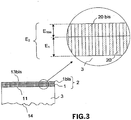
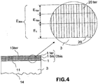
- the figure 1 is a sectional view and an enlarged view of the initial nonlinear optical network 1.
- This network 1 comprises a plurality of layers 20 whose linear coefficients vary from one layer to the next layer.
- This network comprises a first face 11 and a second face 12 substantially parallel. There are various methods for producing said initial network.
- the non-linear material is deposited on a seed substrate 3.
- This comprises a crystalline material having a first crystalline orientation, the upper face 11 of the seed substrate having a thin structure, said structure being constituted by a so-called precursor network parallel strips of the same crystalline material and of inverse crystalline orientation of that of the crystalline material of the seed substrate 3.
- the deposition is carried out, for example, by the epitaxial growth method HVPE (Hydride Vapor Phase Epitaxy) on the upper face 11 of the seed substrate.
- HVPE Hydrodride Vapor Phase Epitaxy
- This thickness comprises, on the one hand, imperfections of the surface 12 on a first thickness E 01 and, on the other hand, structural imperfections on a second thickness E 02 due, for example, to variations in the speed of growth of the various layers during the deposit or initial defects of the seed substrate.
- the first step of the production method consists in determining the useful thickness E 1. Since the thicknesses of the various layers are of the order of a few microns to a few tens of microns, the means of determining the thickness comprising imperfections are optical display devices. The observation by the edge of the initial network makes it possible to determine the thicknesses E 0 , E 01 and E 02 . A possible cut can be made in the substrate so that the network is flush with the substrate after cutting, thus improving the observation. An optional chemical revelation may also be performed to improve the contrast.
- preliminary preparation steps can be performed to facilitate said step.
- the second step of the production method consists, in a first step, in smoothing the face 12 by mechanical abrasion so as to eliminate the surface disturbances present in the thicknesses E 01 and E 02 ; then, in a second step, to complete this first mechanical grinding operation with a second chemical-mechanical polishing operation and to obtain a quality of surface area sufficient to produce an epitaxial deposit.
- the polished plane face 13 is thus obtained substantially perpendicular to the mean plane of the layers of the grating 1.
- This second operation may be superfluous under certain conditions of epitaxial deposition by the HVPE method.
- the first network has been made on a large substrate, typically greater than 50 millimeters in diameter (equivalent to a standard "wafer" diameter of 2 inches in English unit), it is possible to polish the face 12 of the network and the underside 14 of the substrate simultaneously in a dual tray device.
- These devices are particularly used in the microelectronics industry to polish semiconductor wafers. It is, however, in this case, more difficult to control the thickness and quality of the resulting network. We proceed then by successive stages until a polished network is obtained which no longer contains structural disturbances.
- the network must not be too fragile.
- a minimum thickness of 50 microns for the network alone and 300 microns for the substrate is desirable; when the initial network has no substrate, a minimum thickness of 350 microns is desirable.
- the second face 12 has become the third flat face 13.
- the thickness of the network is now E 1 .
- the surface 13 is cleaned and controlled, for example by optical means, to verify that the network is ready for use for epitaxial deposits under conditions that preserve the structure of the network.
- the quality of the preparation of its surface can also make it possible to manufacture by epitaxy, by the OMCVD or MBE methods, structures which are co-integrated with waveguides with non-linear optical network such as laser diodes, optical modulators, Bragg grating sections.
- nonlinear optical networks There are different possible materials for making nonlinear optical networks. It is possible to use, for example, a crystal belonging to the cubic crystallographic class 43m.
- the susceptibility tensor is shown below for this crystallographic class: 0 0 0 d 0 0 0 0 0 0 d 0 0 0 0 0 0 d
- This crystal can be either gallium arsenide (AsGa) or indium phosphide (InP) or cadmium telluride (CdTe) or zinc selenide (ZnSe) or zinc telluride (ZnTe) or phosphide of gallium (GaP) or indium arsenide (InAs) or indium antimonide (InSb).
- AsGa gallium arsenide
- InP indium phosphide
- CdTe cadmium telluride
- ZnSe zinc selenide
- ZnTe zinc telluride
- the material may also be tellurium (Te) or selenium (Se) or gallium nitride (GaN).
- GaAlAs gallium aluminum arsenide
Landscapes
- Physics & Mathematics (AREA)
- Nonlinear Science (AREA)
- Optics & Photonics (AREA)
- Chemical & Material Sciences (AREA)
- General Physics & Mathematics (AREA)
- Engineering & Computer Science (AREA)
- Crystallography & Structural Chemistry (AREA)
- Nanotechnology (AREA)
- Life Sciences & Earth Sciences (AREA)
- Biophysics (AREA)
- Optical Integrated Circuits (AREA)
- Optical Modulation, Optical Deflection, Nonlinear Optics, Optical Demodulation, Optical Logic Elements (AREA)
Claims (10)
- Verfahren zum Realisieren eines dicken nichtlinearen optischen Gitters (2) mit einer Dicke von mehreren 100 Mikron auf der Basis eines anfänglichen nichtlinearen optischen Gitters (1), wobei die Dicke (E2) des nichtlinearen optischen Gitters (2) größer ist als die Dicke (E0) des anfänglichen nichtlinearen optischen Gitters (1), wobei das anfängliche Gitter wenigstens eine Mehrzahl von ebenen und zueinander parallelen Schichten (20) umfasst, wobei die Schichten wenigstens zwei nichtlineare, nach algebraischen Werten unterschiedliche Koeffizienten hat, wobei das anfängliche Gitter eine erste Fläche (11) und eine zweite Fläche (12) hat, die im Wesentlichen parallel zueinander und im Wesentlichen senkrecht zur Mittelebene der Schichten sind, wobei die zweite Fläche (12) frei ist, dadurch gekennzeichnet, dass es die folgenden Realisierungsschritte beinhaltet:• einen ersten Schritt des Bestimmens der Dicke (E01, E02) des oberen Teils des anfänglichen Gitters (1), der sich unter der zweiten Fläche (12) befindet, die Strukturoberflächenimperfektionen aufweist;• einen zweiten Schritt des Polierens der zweiten Fläche (12) des anfänglichen Gitters (1), so dass der die Imperfektionen aufweisende obere Teil eliminiert und eine polierte und ebene dritte Fläche (13) erhalten werden kann, wobei die Fläche im Wesentlichen senkrecht zur Mittelebene der Schichten (20) ist;• einen dritten Schritt des Reinigens und Kontrollierens der dritten Fläche (13);• wenigstens einen vierten Schritt des epitaxialen Absetzens von wenigstens einer abgesetzten Materialschicht (1bis, 1ter) auf die dritte Fläche (13), wobei das epitaxiale Wachstum in der abgesetzten Schicht eine Struktur ähnlich der Zelle des anfänglichen Gitters reproduziert, wobei die Baugruppe aus dem anfänglichen Gitter (1) und der abgesetzten Schicht (1bis, 1ter) das nichtlineare optische Gitter (2) bildet.
- Verfahren zum Realisieren eines optischen Gitters (2) nach Anspruch 1, dadurch gekennzeichnet, dass die Mittel zum Bestimmen der Dicke, die Imperfektionen umfasst, optische Visualisierungsvorrichtungen sind.
- Verfahren zum Realisieren eines nichtlinearen optischen Gitters (2) nach einem der vorherigen Ansprüche, dadurch gekennzeichnet, dass die Dicke (E1) des anfänglichen optischen Gitters nach dem zweiten Realisierungsschritt wenigstens 50 Mikron beträgt.
- Verfahren zum Realisieren eines nichtlinearen optischen Gitters (2) nach Anspruch 1, dadurch gekennzeichnet, dass das anfängliche nichtlineare optische Gitter (1) durch ein Keimsubstrat (3) getragen wird, das eine untere Fläche (14) und eine ebene obere Fläche (11) aufweist, wobei die obere Fläche (11) des Keimsubstrats mit der ersten Fläche (11) des anfänglichen nichtlinearen optischen Gitters (1) zusammenfällt.
- Verfahren zum Realisieren eines nichtlinearen optischen Gitters (2) nach Anspruch 4, dadurch gekennzeichnet, dass das Keimsubstrat (3) ein kristallines Material mit einer ersten Kristallorientierung hat, wobei die obere Fläche (11) des Keimsubstrats eine Struktur von geringer Dicke hat, wobei die Struktur von einem Vorläufergitter mit parallelen Banden desselben kristallinen Materials und mit einer Kristallorientierung umgekehrt zu der Zelle des Keimsubstrats (3) gebildet wird.
- Verfahren zum Realisieren eines nichtlinearen optischen Gitters (2) nach Anspruch 5, dadurch gekennzeichnet, dass die Dicke des Keimsubstrats (3) wenigstens 300 Mikron beträgt.
- Verfahren zum Realisieren eines optischen Gitters (2) nach Anspruch 4, dadurch gekennzeichnet, dass der zweite Realisierungsschritt die folgenden Vorabschritte beinhaltet:• einen ersten Vorabschritt des Glättens der unteren Fläche (14) des Substrats;• einen zweiten Vorabschritt des Klebens wenigstens der unteren Fläche (14) auf wenigstens einen ebenen Träger (32), wobei die Platzierung des Trägers die Manipulation des anfänglichen optischen Gitters (1) für die späteren Poliervorgänge erleichtert.
- Verfahren zum Realisieren eines nichtlinearen optischen Gitters (2) nach Anspruch 4, dadurch gekennzeichnet, dass das anfängliche nichtlineare optische Gitter (1) mit dem epitaxialen Wachstumsverfahren HVPE (Hydriddampphasenepitaxie) auf der oberen Fläche des Keimsubstrats (3) erhalten wird.
- Verfahren zum Realisieren eines optischen Gitters (2) nach einem der vorherigen Ansprüche, dadurch gekennzeichnet, dass im Laufe des vierten Realisierungsschritts wenigstens zwei Materialschichten (1bis, 1ter) mit einem anderen optischen Index abgesetzt werden, um einen optischen Wellenleiter zu bilden.
- Verfahren zum Realisieren eines nichtlinearen optischen Gitters (2) nach einem der vorherigen Ansprüche, dadurch gekennzeichnet, dass im Laufe des vierten Realisierungsschrittes wenigstens eine der Schichten (1bis, 1ter) mit dem epitaxialen Wachstumsverfahren OMCVD (metallorganische chemische Dampfphasenabscheidung) oder MBE (Molekularstrahlepitaxie) erhalten wird.
Applications Claiming Priority (3)
| Application Number | Priority Date | Filing Date | Title |
|---|---|---|---|
| FR0215075A FR2847990B1 (fr) | 2002-11-29 | 2002-11-29 | Procede de realisation de reseaux optiques non lineaires epais |
| FR0215075 | 2002-11-29 | ||
| PCT/EP2003/050882 WO2004051360A2 (fr) | 2002-11-29 | 2003-11-24 | Procede de realisation de reseaux optiques non lineaires epais |
Publications (2)
| Publication Number | Publication Date |
|---|---|
| EP1565786A2 EP1565786A2 (de) | 2005-08-24 |
| EP1565786B1 true EP1565786B1 (de) | 2016-12-21 |
Family
ID=32309863
Family Applications (1)
| Application Number | Title | Priority Date | Filing Date |
|---|---|---|---|
| EP03789450.8A Expired - Lifetime EP1565786B1 (de) | 2002-11-29 | 2003-11-24 | Prozess zur herstellung von dicken optischen nichtlineargittern |
Country Status (5)
| Country | Link |
|---|---|
| US (1) | US20060139651A1 (de) |
| EP (1) | EP1565786B1 (de) |
| AU (1) | AU2003294035A1 (de) |
| FR (1) | FR2847990B1 (de) |
| WO (1) | WO2004051360A2 (de) |
Family Cites Families (3)
| Publication number | Priority date | Publication date | Assignee | Title |
|---|---|---|---|---|
| KR0137125B1 (ko) * | 1992-11-16 | 1998-06-15 | 모리시타 요이찌 | 광도파로소자와 그 제조방법 |
| FR2704953B1 (fr) * | 1993-05-03 | 1995-06-23 | Thomson Csf | Reseau optique non-lineaire et procede de realisation. |
| US5802232A (en) * | 1996-02-16 | 1998-09-01 | Bell Communications Research, Inc. | Bonded structure with portions of differing crystallographic orientations, particularly useful as a non linear optical waveguide |
-
2002
- 2002-11-29 FR FR0215075A patent/FR2847990B1/fr not_active Expired - Lifetime
-
2003
- 2003-11-24 EP EP03789450.8A patent/EP1565786B1/de not_active Expired - Lifetime
- 2003-11-24 AU AU2003294035A patent/AU2003294035A1/en not_active Abandoned
- 2003-11-24 WO PCT/EP2003/050882 patent/WO2004051360A2/fr not_active Ceased
- 2003-11-24 US US10/536,696 patent/US20060139651A1/en not_active Abandoned
Also Published As
| Publication number | Publication date |
|---|---|
| FR2847990A1 (fr) | 2004-06-04 |
| AU2003294035A1 (en) | 2004-06-23 |
| FR2847990B1 (fr) | 2005-02-18 |
| AU2003294035A8 (en) | 2004-06-23 |
| US20060139651A1 (en) | 2006-06-29 |
| EP1565786A2 (de) | 2005-08-24 |
| WO2004051360A2 (fr) | 2004-06-17 |
| WO2004051360A3 (fr) | 2004-08-19 |
Similar Documents
| Publication | Publication Date | Title |
|---|---|---|
| EP2628243B1 (de) | Heterogene akustische struktur aus einem homogenen material | |
| Jiang et al. | Suspended gallium arsenide platform for building large scale photonic integrated circuits: passive devices | |
| FR2909491A1 (fr) | Dispositif laser a source laser et guide d'onde couples | |
| US8619356B1 (en) | Multi-layer gallium arsenide-based fresnel phase-shift device for infrared wavelength conversion | |
| EP1966821B1 (de) | Verfahren zum relaxieren eines verspannten dünnfilms | |
| EP1565786B1 (de) | Prozess zur herstellung von dicken optischen nichtlineargittern | |
| EP0949516A1 (de) | Elektrooptisches Verfahren zur Signalverarbeitung, Vorrichtung zur Durchführung des Verfahrens und Anwendung | |
| EP4198587B1 (de) | Verfahren zur herstellung eines photonischen chips | |
| US20230084321A1 (en) | Nonlinear on-chip optical devices using alscn | |
| Liu et al. | Second-order optical nonlinearities in ferroelectric ScAlN for quantum photonics | |
| EP3968064A1 (de) | Optische filtervorrichtung | |
| Spettel et al. | Ultraviolet to mid-infrared optical properties of sputtered Al (Sc) N-on-SiO2 thin films and experimental demonstration of AlN integrated photonic devices in the telecom C-band | |
| Tassev et al. | Homo and heteroepitaxial growth and study of orientation-patterned GaP for nonlinear frequency conversion devices | |
| US7812423B2 (en) | Optical device comprising crystalline semiconductor layer and reflective element | |
| Marris-Morini et al. | Germanium-Based Mid-Infrared Photonics | |
| FR2574566A1 (fr) | Diodes emettrices/receptrices de lumiere et elements de transmission optiques non reciproques integres, et leur procede de fabrication | |
| EP0736791B1 (de) | Photorefraktives Quantentopfbauelement | |
| FR2704953A1 (fr) | Réseau optique non-linéaire et procédé de réalisation. | |
| Xu et al. | AlGaAs semiconductor quasiphase-matched wavelength converters | |
| WO2003029893A2 (en) | Non-linear optical stacks | |
| Eyres et al. | Demonstration of second harmonic generation in all-epitaxially grown orientation-patterned AIGaAs waveguides | |
| EP4474890A1 (de) | Elektrooptische vorrichtung und verfahren zur herstellung einer elektrooptischen vorrichtung | |
| Liu et al. | $\text {ScAlN}/\text {Si} _ {3}~\mathrm {N} _ {4} $ for an Ultralow Loss, Multi-Functional Quantum Photonic Integration Platform | |
| Lallier et al. | Quasi-phase-matched nonlinear crystals for infrared frequency conversion | |
| Oliveira | Photonic integrated circuit (PIC) devices for inter-and intra-chip optical communication using GeSn alloy layers grown on Silicon substrates |
Legal Events
| Date | Code | Title | Description |
|---|---|---|---|
| PUAI | Public reference made under article 153(3) epc to a published international application that has entered the european phase |
Free format text: ORIGINAL CODE: 0009012 |
|
| 17P | Request for examination filed |
Effective date: 20050531 |
|
| AK | Designated contracting states |
Kind code of ref document: A2 Designated state(s): AT BE BG CH CY CZ DE DK EE ES FI FR GB GR HU IE IT LI LU MC NL PT RO SE SI SK TR |
|
| AX | Request for extension of the european patent |
Extension state: AL LT LV MK |
|
| DAX | Request for extension of the european patent (deleted) | ||
| RBV | Designated contracting states (corrected) |
Designated state(s): DE GB IT SE |
|
| GRAP | Despatch of communication of intention to grant a patent |
Free format text: ORIGINAL CODE: EPIDOSNIGR1 |
|
| INTG | Intention to grant announced |
Effective date: 20160616 |
|
| GRAS | Grant fee paid |
Free format text: ORIGINAL CODE: EPIDOSNIGR3 |
|
| GRAA | (expected) grant |
Free format text: ORIGINAL CODE: 0009210 |
|
| RAP1 | Party data changed (applicant data changed or rights of an application transferred) |
Owner name: THALES |
|
| AK | Designated contracting states |
Kind code of ref document: B1 Designated state(s): DE GB IT SE |
|
| REG | Reference to a national code |
Ref country code: GB Ref legal event code: FG4D Free format text: NOT ENGLISH |
|
| REG | Reference to a national code |
Ref country code: DE Ref legal event code: R096 Ref document number: 60349746 Country of ref document: DE |
|
| REG | Reference to a national code |
Ref country code: SE Ref legal event code: TRGR |
|
| PG25 | Lapsed in a contracting state [announced via postgrant information from national office to epo] |
Ref country code: IT Free format text: LAPSE BECAUSE OF FAILURE TO SUBMIT A TRANSLATION OF THE DESCRIPTION OR TO PAY THE FEE WITHIN THE PRESCRIBED TIME-LIMIT Effective date: 20161221 |
|
| REG | Reference to a national code |
Ref country code: DE Ref legal event code: R097 Ref document number: 60349746 Country of ref document: DE |
|
| PLBE | No opposition filed within time limit |
Free format text: ORIGINAL CODE: 0009261 |
|
| STAA | Information on the status of an ep patent application or granted ep patent |
Free format text: STATUS: NO OPPOSITION FILED WITHIN TIME LIMIT |
|
| 26N | No opposition filed |
Effective date: 20170922 |
|
| PGFP | Annual fee paid to national office [announced via postgrant information from national office to epo] |
Ref country code: SE Payment date: 20221026 Year of fee payment: 20 Ref country code: GB Payment date: 20221013 Year of fee payment: 20 Ref country code: DE Payment date: 20221018 Year of fee payment: 20 |
|
| REG | Reference to a national code |
Ref country code: DE Ref legal event code: R071 Ref document number: 60349746 Country of ref document: DE |
|
| REG | Reference to a national code |
Ref country code: GB Ref legal event code: PE20 Expiry date: 20231123 |
|
| REG | Reference to a national code |
Ref country code: SE Ref legal event code: EUG |
|
| PG25 | Lapsed in a contracting state [announced via postgrant information from national office to epo] |
Ref country code: GB Free format text: LAPSE BECAUSE OF EXPIRATION OF PROTECTION Effective date: 20231123 |
|
| PG25 | Lapsed in a contracting state [announced via postgrant information from national office to epo] |
Ref country code: GB Free format text: LAPSE BECAUSE OF EXPIRATION OF PROTECTION Effective date: 20231123 |