EP1564986A2 - Solid-state image pickup device and driving method therefor - Google Patents
Solid-state image pickup device and driving method therefor Download PDFInfo
- Publication number
- EP1564986A2 EP1564986A2 EP05002973A EP05002973A EP1564986A2 EP 1564986 A2 EP1564986 A2 EP 1564986A2 EP 05002973 A EP05002973 A EP 05002973A EP 05002973 A EP05002973 A EP 05002973A EP 1564986 A2 EP1564986 A2 EP 1564986A2
- Authority
- EP
- European Patent Office
- Prior art keywords
- image pickup
- output circuits
- solid
- pickup device
- state image
- Prior art date
- Legal status (The legal status is an assumption and is not a legal conclusion. Google has not performed a legal analysis and makes no representation as to the accuracy of the status listed.)
- Granted
Links
Images


Classifications
-
- H—ELECTRICITY
- H04—ELECTRIC COMMUNICATION TECHNIQUE
- H04N—PICTORIAL COMMUNICATION, e.g. TELEVISION
- H04N25/00—Circuitry of solid-state image sensors [SSIS]; Control thereof
- H04N25/40—Extracting pixel data from image sensors by controlling scanning circuits, e.g. by modifying the number of pixels sampled or to be sampled
- H04N25/46—Extracting pixel data from image sensors by controlling scanning circuits, e.g. by modifying the number of pixels sampled or to be sampled by combining or binning pixels
-
- H—ELECTRICITY
- H04—ELECTRIC COMMUNICATION TECHNIQUE
- H04N—PICTORIAL COMMUNICATION, e.g. TELEVISION
- H04N25/00—Circuitry of solid-state image sensors [SSIS]; Control thereof
- H04N25/70—SSIS architectures; Circuits associated therewith
- H04N25/76—Addressed sensors, e.g. MOS or CMOS sensors
- H04N25/767—Horizontal readout lines, multiplexers or registers
-
- H—ELECTRICITY
- H04—ELECTRIC COMMUNICATION TECHNIQUE
- H04N—PICTORIAL COMMUNICATION, e.g. TELEVISION
- H04N25/00—Circuitry of solid-state image sensors [SSIS]; Control thereof
- H04N25/70—SSIS architectures; Circuits associated therewith
- H04N25/76—Addressed sensors, e.g. MOS or CMOS sensors
- H04N25/78—Readout circuits for addressed sensors, e.g. output amplifiers or A/D converters
Definitions
- the present invention relates to solid-state image pickup devices and driving methods for solid-state image pickup devices, and more particularly, to horizontal-scanning solid-state image pickup devices and driving methods for horizontal-scanning solid-state image pickup devices.
- a solid-state image pickup device for example, in contrast with a still image mode in which information of all pixels of the solid-state image pickup device is used, the resolution is reduced by adding pixel information or by skipping pixel information in a monitor mode in which an object is monitored. Accordingly, in a solid-state image pickup device for reading pixel information at a low resolution, pixel information of a plurality of pixels in the horizontal direction (lateral direction) in a horizontal signal line has been added by activating horizontal scanning pulses ⁇ H for a plurality of columns at the same time using a horizontal scanning circuit and by accessing the plurality of columns at the same time. (See, for example, Japanese Unexamined Patent Application Publication No. 11-146278.)
- the solid-state image pickup device since the solid-state image pickup device according to the known example has an arrangement in which pixels in the horizontal direction are added, if this solid-state image pickup device is used as an image pickup device of a digital still camera, this arrangement cannot be applied to a monitor mode in which pixel addition in the vertical direction (longitudinal direction) is also required. In addition, since pixel information must be read for each row through a horizontal signal line, this arrangement cannot cope with an increase in the speed of reading all pixels in the still image mode.
- a solid-state image pickup device includes a pixel array area in which pixels are two-dimensionally arranged in a matrix, the pixels each including a photoelectric conversion portion; a plurality of capacitors for storing electric charges of the pixels in a plurality of rows for each column, the electric charges being output from the pixel array area via a vertical signal line; a plurality of output circuits for outputting analog signals corresponding to the electric charges stored in the plurality of capacitors; and a switching unit for selectively short-circuiting input terminals of the plurality of output circuits.
- a first driving mode in which the switching unit is not short-circuited so that the analog signals are read independently from the plurality of output circuits and a second driving mode in which the switching unit is short-circuited so that an average of the analog signals is read from the plurality of output circuits are appropriately and selectively set.
- the solid-state image pickup device in the first driving mode, since analog signals corresponding to electric charges stored in a plurality of capacitors are output through a plurality of output circuits independently, information of pixels in a plurality of rows can be read in parallel. Also, in the second driving mode, since input terminals of the plurality of output circuits are short-circuited, information of pixels in a plurality of rows is added for each pixel, and an average, that is, not merely a sum is read.
- this mode can cope with an increase in the speed of reading information of all pixels.
- the second driving mode since information of pixels in a plurality of rows is added for each pixel and an average is read, pixel addition in the vertical direction can be realized.
- Fig. 1 is a schematic diagram showing the structure of a solid-state image pickup device according to an embodiment of the present invention.
- MOS metal-oxide semiconductor
- pixels (pixel circuits) 11 each include a photoelectric conversion portion, for example, a photo-diode PD.
- a pixel array area 12 includes m row x n column pixels arranged in a two-dimensional array.
- transfer control lines 13-1 to 13-m and reset control lines 14-1 to 14-m are provided for corresponding rows, and vertical signal lines 15-1 to 15-n are provided for corresponding columns.
- Each of the pixels 11 has an arrangement having three transistors.
- Each of the pixels 11 includes, for example, a transfer transistor Q11, an amplifier transistor Q12, and a reset transistor Q13, in addition to the photo-diode PD.
- the transfer transistor Q11, the amplifier transistor Q12, and the reset transistor Q13 are, for example, N-channel MOS transistors.
- the anode of the photo-diode PD is grounded.
- the source of the transfer transistor Q11 is connected to the cathode of the photo-diode PD, the drain of the transfer transistor Q11 is connected to a floating diffusion (FD) portion, and the gate of the transfer transistor Q11 is connected to the corresponding transfer control lines 13-1 to 13-m. Accordingly, the transfer transistor Q11 transfers a signal charge (photoelectron) obtained by photoelectric conversion in the photo-diode PD to the FD portion.
- the FD portion is a diffusion layer having a parasitic capacitance.
- the gate of the amplifier transistor Q12 is connected to the FD portion, the drain of the amplifier transistor Q12 is connected to a drain potential DRN, and the source of the amplifier transistor Q12 is connected to the corresponding vertical signal lines 15-1 to 15-n. Accordingly, the amplifier transistor Q12 outputs a signal (reset level/signal level) corresponding to the potential of the FD portion to the corresponding vertical signal lines 15-1 to 15-n.
- the source of the reset transistor Q13 is connected to the FD portion, the drain of the reset transistor Q13 is connected to the drain potential DRN, and the gate of the reset transistor Q13 is connected to the corresponding reset control lines 14-1 to 14-m. Accordingly, the reset transistor Q13 resets the potential of the FD portion to the drain potential DRN.
- each of the pixels (pixel circuits) 11 having three transistors is described here, the arrangement is not limited to this.
- each of the pixels (pixel circuits) 11 may have an arrangement having four transistors including, for example, a selection transistor for selecting a pixel.
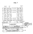
- a vertical driving circuit 16 a column circuit 17 functioning as signal processing means, a horizontal scanning circuit 18 and a horizontal selection switch control circuit 19 functioning as a horizontal driving circuit, and an output circuit unit 20 are provided near the pixel array area 12.
- the vertical driving circuit 16 includes, for example, shift registers.
- the vertical driving circuit 16 selects the pixels 11 of the pixel array area 12 for each row, and gives transfer signals TRF via the corresponding transfer control lines 13-1 to 13-m and reset signals RST via the corresponding reset control lines 14-1 to 14-m to the pixels 11 in the selected row.
- the pixels 11 are selected for each row by giving a selection signal SEL from the vertical driving circuit 16 to a power supply control circuit (not shown) in synchronization with vertical scanning and, in response to this, by supplying the drain potential DRN to the pixels 11 in the selected row from the power supply control circuit.
- Fig. 2 shows the timing relationship among the selection signal SEL, the drain potential DRN, the reset signal RST, and the transfer signal TRF.
- the pixels 11 are selected for each row in accordance with the selection signal SEL. Then, in the selected row, giving the reset signal RST to the pixels 11 causes the potential of the FD portion to be reset to the drain potential DRN, and the reset potential of the FD portion is output as a reset level to the corresponding vertical signal lines 15-1 to 15-n via the amplifier transistor Q12.
- giving the transfer signal TRF to the pixels 11 causes a signal charge that is photo-electrically converted in the photo-diode PD to be transferred to the FD portion, and the transferred potential of the FD portion is output as a signal level to the corresponding vertical signal lines 15-1 to 15-n via the amplifier transistor Q12.
- the column circuit 17 is a signal processing circuit including, for example, a correlated double sampling (CDS) circuit and a sample-and-hold (S/H) circuit.
- CDS correlated double sampling
- S/H sample-and-hold
- the column circuit 17 loads a reset level and a signal level output, for example, from the pixels 11 in two selected rows of the pixel array area 12 for each column during a horizontal blanking period and obtains the difference between the levels. Accordingly, the column circuit 17 eliminates fixed pattern noise of the pixels 11 and samples-and-holds electric charges of the pixels in the two rows.
- Fig. 3 shows an example of the arrangement of the S/H circuit part for a column in the column circuit'17.
- the S/H circuit part for the column in the column circuit 17 has an arrangement including, between the vertical signal line 15 and a reference potential, for example, a ground potential, a sampling switch 31-1 and a capacitor 32-1 connected in series with each other and a sampling switch 31-2 and a capacitor 32-2 connected in series with each other.
- the sampling switches 31-1 and 31-2 sample signals of the pixels in the two rows supplied through the vertical signal line 15 and store the sampled signals in the capacitors 32-1 and 32-2.
- two horizontal signal lines 21-1 and 21-2 are provided. Also, a horizontal selection switch 22-1 is connected between the horizontal signal line 21-1 and a common connection node N11 of the sampling switch 31-1 and the capacitor 32-1, and a horizontal selection switch 22-2 is connected between the horizontal signal line 21-2 and a common connection node N12 of the sampling switch 31-2 and the capacitor 32-2.
- the horizontal selection switches 22-1 and 22-2 constitute a horizontal driving circuit, together with the horizontal scanning circuit 18 and the horizontal selection switch control circuit 19.
- the horizontal scanning circuit 18 includes, for example, shift registers.
- the horizontal scanning circuit 18 outputs horizontal scanning pulses ⁇ H1 to ⁇ Hn in order during a horizontal scanning period (effective pixel period).
- the horizontal selection switch control circuit 19 sequentially outputs dual-rail switch control pulses ⁇ S1-1 and ⁇ S1-2 to ⁇ Sn-1 and ⁇ Sn-2 and controls driving of the horizontal selection switches 22-1 and 22-2.
- the horizontal selection switches 22-1 and 22-2 enter an on state (closed state) by receiving the switch control pulses ⁇ S1-1 and ⁇ S1-2 to ⁇ Sn-1 and ⁇ Sn-2.
- the horizontal selection switches 22-1 and 22-2 supply electric charges stored in the capacitors 32-1 and 32-2 to the output circuit unit 20 via the horizontal signal lines 21-1 and 21-2.
- Fig. 3 is a circuit diagram showing an example of the arrangement of the S/H circuit part for a column and the arrangement of the output circuit unit 20.
- the output circuit unit 20 includes two output circuits, for example, charge-voltage conversion amplifiers 23-1 and 23-2, provided so as to correspond to the horizontal signal lines 21-1 and 21-2; S/H circuits 24-1 and 24-2 provided at an output side of the charge-voltage conversion amplifiers 23-1 and 23-2; a switch 25 for selectively short-circuiting input terminals of the charge-voltage conversion amplifiers 23-1 and 23-2; and a switch 26 for selectively short-circuiting output terminals of the charge-voltage conversion amplifiers 23-1 and 23-2.
- the switch 26 is not essential. The reason why the switch 26 is not essential will be described below.
- the charge-voltage conversion amplifier 23-1 includes an operational amplifier 41 whose inverting (-) input terminal is connected to an output terminal of the horizontal signal line 21-1 and whose non-inverting (+) input terminal receives a reference voltage Vref; a switch 42a, a feedback capacitor 43, and a switch 42b connected in series with each other between the inverting input terminal and the output terminal of the operational amplifier 41; and a reset switch 44 connected between the inverting input terminal and the output terminal of the operational amplifier 41.
- the charge-voltage conversion amplifier 23-1 converts an electric charge supplied via the horizontal signal line 21-1 into a voltage.
- k (k is an integer equal to 2 or more) switches 42a1 to 42ak, feedback capacitors 43-1 to 43-k, and switches 42b1 to 42bk are provided so as to set the gain of the charge-voltage conversion amplifier 23-1.
- the charge-voltage conversion amplifier 23-2 has the same arrangement as the charge-voltage conversion amplifier 23-1.
- the S/H circuits 24-1 and 24-2 sample-and-hold data of output signals of the charge-voltage conversion amplifiers 23-1 and 23-2.
- Hold data (pixel data) of the S/H circuits 24-1 and 24-2 is derived from dual output terminals 27-1 and 27-2 as pixel signals (analog signals) corresponding to electric charges photo-electrically converted at the pixels 11.
- the switches 25 and 26 are associated with each other.
- the switches 25 and 26 enter an on state (closed state) in response to a mode signal for designating the driving mode, and the input terminals of the charge-voltage conversion amplifiers 23-1 and 23-2 and the output terminals of the charge-voltage conversion amplifiers 23-1 and 23-2 are short-circuited.
- Vm represents a potential corresponding to an electric charge stored in a capacitor 32-1i in a column i
- Vref represents a reference potential of the charge-voltage conversion amplifier 23-1.
- the reset switch 44 is turned off, and the horizontal selection switch 22-1i is turned on in response to a switch control pulse ⁇ Si-1 that is synchronized with the horizontal scanning pulse ⁇ H.
- the capacitor 32-1i is connected to the horizontal signal line 21-1 via the horizontal selection switch 22-1i.
- the amount of change (the amount of difference) ⁇ Q ( Q1 - Q2) in the electric charge appears at the feedback capacitor 43 of the charge-voltage conversion amplifier 23-1.
- the solid-state image pickup device has an arrangement including dual capacitors, that is, the capacitors 32-1 and 32-2, and dual charge-voltage conversion amplifiers, that is, the charge-voltage conversion amplifiers 23-1 and 23-2.
- dual capacitors that is, the capacitors 32-1 and 32-2
- dual charge-voltage conversion amplifiers that is, the charge-voltage conversion amplifiers 23-1 and 23-2.
- pixel addition in the vertical direction can be performed using the same circuits. More specifically, turning on the switch 25 and short-circuiting the input terminals of the charge-voltage conversion amplifiers 23-1 and 23-2 enables addition of two pixels in the vertical direction. Accordingly, when short-circuiting the input terminals of the charge-voltage conversion amplifiers 23-1 and 23-2 causes an offset of each of the dual charge-voltage conversion amplifiers 23-1 and 23-2 to be ignored, basically, with respect to outputs of the charge-voltage conversion amplifiers 23-1 and 23-2, analog image signals for two rows are added for each pixel. Thus, an average, that is, not merely a sum, is obtained, and each output exhibits the same value.
- an averaged pixel signal obtained by pixel addition can be read from either the analog output terminal 27-1 or 27-2.
- a load viewed from the S/H circuit 24-1 or 24-2 whose switch is turned off is low, this achieves high-speed reading.
- the switch 26 by turning on the switch 26 in association with the switch 25 and by short-circuiting the output terminals of the charge-voltage conversion amplifiers 23-1 and 23-2 as well as the input terminals of the charge-voltage conversion amplifiers 23-1 and 23-2, even if offsets are found in the dual charge-voltage conversion amplifiers 23-1 and 23-2, an average in which the offsets are canceled can be output.
- the two charge-voltage amplifiers function as a large charge-voltage conversion amplifier.
- the switch 25 for selectively short-circuiting the input terminals of the charge-voltage conversion amplifiers 23-1 and 23-2 is provided, and the switch 26 for selectively short-circuiting the output terminals of the charge-voltage conversion amplifiers 23-1 and 23-2 is preferably provided.
- the MOS solid-state image pickup device can be selectively driven in two modes, a first driving mode in which the switches 25 and 26 are in a non-short-circuit state (off state) so that the analog signals are read independently from the charge-voltage conversion amplifiers 23-1 and 23-2 and a second driving mode in which the switches 25 and 26 are in a short-circuit state (on state) so that an average of the analog signals is read from the charge-voltage conversion amplifiers 23-1 and 23-2.
- the switches 25 and 26 are turned off, and the input terminals and the output terminals of the charge-voltage conversion amplifiers 23-1 and 23-2 enter a non-short-circuit state.
- the dual-rail circuits can be used as dual-rail outputs, and analog image signals for two rows can be read from the analog output terminals 27-1 and 27-2 independently and in parallel. Accordingly, by adopting the form of dual-rail outputs, high-speed reading can be realized when pixel information of all pixels is read in a still image mode or the like.
- the dual-rail output form is not necessarily used.
- a single-rail output form may be adopted by using only one of the dual capacitors 32-1 and 32-2 and using only one of the two charge-voltage conversion amplifiers 23-1 and 23-2.
- the switch 25 is turned on and the input terminals of the charge-voltage conversion amplifiers 23-1 and 23-2 enter a short-circuit state.
- analog pixel signals for two rows are added for each pixel, and an average, that is, not merely a sum, can be read.
- the switch 26 is turned on and the output terminals of the charge-voltage conversion amplifiers 23-1 and 23-2 enter a short-circuit state.
- the offsets can be canceled. Therefore, an average not including an offset can be output. Accordingly, by adding two pixels in the vertical direction, reading at a low resolution can be realized.
- dual-rail capacitors 32-1 and 32-2 and the dual-rail charge-voltage conversion amplifiers 23-1 and 23-2 are not necessarily used.
- Three- or more-rail capacitors and three- or more-rail charge-voltage conversion amplifiers may be provided to add three or more pixels in the vertical direction for achieving reading at a lower resolution.
- f-rail outputs can be realized in the first driving mode and addition of f pixels in the vertical direction can be realized in the second driving mode.
- a charge-voltage conversion amplifier including an operational amplifier 51 whose non-inverting input receives the reference voltage Vref, an input resistor 52 connected to an inverting input terminal of the operational amplifier 51, and a feedback resistor 53 connected between an output terminal and the inverting input terminal of the operational amplifier 51 may be used.
- the input resistor 52 is provided for prevention of oscillation, and does not contribute to operation.
- current-voltage conversion amplifiers 50 are used as output circuits and input terminals and output terminals are short-circuited in the second driving mode, two feedback resistors 53-1 and 53-2 are connected in parallel to each other, and a combined resistance R/2 is obtained.
- the present invention can also be applied to a MOS solid-state image pickup device in which, for example, for the purpose of noise reduction, the capacitors 32-1 and 32-2 and the charge-voltage conversion amplifiers 23-1 and 23-2 are provided for each of the vertical signal lines 15-1 to 15-n and in which electric charges output from the capacitors 32-1 and 32-2 are converted into voltages by the charge-voltage conversion amplifiers 23-1 and 23-2 and output to the horizontal signal lines 21-1 and 21-2.
- the S/H circuits 24-1 and 24-2 are provided in the horizontal signal lines 21-1 and 21-2. Since the switch 25 is provided between the input terminals of the charge-voltage conversion amplifiers 23-1 and 23-2 for the corresponding vertical signal lines 15-1 to 15-n and the switch 26 is provided between the horizontal signal lines 21-1 and 21-2, the input terminals and the output terminals of the charge-voltage conversion amplifiers 23-1 and 23-2 provided for the corresponding signal lines 15-1 to 15-n can be short-circuited in the second driving mode. Thus, a similar advantage as in the foregoing embodiment can be achieved.
- the present invention can also be applied to a horizontal-scanning charge-coupled device (CCD) solid-state image pickup device, as shown in Fig.
- CCD charge-coupled device
- a solid-state image pickup device may be used as an image pickup device of a camera module, such as a digital still camera, having a still image mode (the first driving mode) and a monitor mode (the second driving mode).
- the solid-state image pickup device according to the present invention may be used as an image pickup device of a portable terminal typified by a cellular telephone having,a camera function having a still image mode and a monitor mode.
Landscapes
- Engineering & Computer Science (AREA)
- Multimedia (AREA)
- Signal Processing (AREA)
- Transforming Light Signals Into Electric Signals (AREA)
- Solid State Image Pick-Up Elements (AREA)
Abstract
Description
Claims (24)
- A solid-state image pickup device comprising:a pixel array area in which pixels are two-dimensionally arranged in a matrix, the pixels each including a photoelectric conversion portion;a plurality of capacitors for storing electric charges of the pixels in a plurality of rows for each column, the electric charges being output from the pixel array area via a vertical signal line;a plurality of output circuits for outputting analog signals corresponding to the electric charges stored in the plurality of capacitors; andfirst switching means for selectively short-circuiting input terminals of the plurality of output circuits.
- The solid-state image pickup device according to Claim 1, further comprising second switching means for selectively short-circuiting output terminals of the plurality of output circuits.
- The solid-state image pickup device according to Claim 1, wherein:the plurality of capacitors and the plurality of output circuits are provided so as to correspond to a plurality of horizontal signal lines; andthe electric charges output from the plurality of capacitors via the plurality of horizontal signal lines are converted into voltages by the plurality of output circuits.
- The solid-state image pickup device according to Claim 1, wherein:the plurality of capacitors and the plurality of output circuits are provided so as to correspond to a plurality of horizontal signal lines; andcurrents corresponding to the electric charges output from the plurality of capacitors via the plurality of horizontal signal lines are converted into voltages by the plurality of output circuits.
- The solid-state image pickup device according to Claim 1, wherein:the plurality of capacitors and the plurality of output circuits are provided for the vertical signal line; andthe electric charges output from the plurality of capacitors are converted into voltages by the plurality of output circuits and output to a plurality of horizontal signal lines.
- A solid-state image pickup device comprising:a pixel array area in which pixels are two-dimensionally arranged in a matrix, the pixels each including a photoelectric conversion portion;a plurality of capacitors for storing electric charges of the pixels in a plurality of rows for each column, the electric charges being output from the pixel array area via a vertical signal line;a plurality of output circuits for outputting analog signals corresponding to the electric charges stored in the plurality of capacitors; andfirst switching means for selectively short-circuiting input terminals of the plurality of output circuits, whereinthe solid-state image pickup device has:a first driving mode in which the first switching means is not short-circuited so that the analog signals are read independently from the plurality of output circuits; anda second driving mode in which the first switching means is short-circuited so that an average of the analog signals is read from the plurality of output circuits.
- The solid-state image pickup device according to Claim 6, further comprising second switching means for selectively short-circuiting output terminals of the plurality of output circuits in association with the first switching means.
- A driving method for a solid-state image pickup device including a pixel array area in which pixels are two-dimensionally arranged in a matrix, the pixels each including a photoelectric conversion portion; a plurality of capacitors for storing electric charges of the pixels in a plurality of rows for each column, the electric charges being output from the pixel array area via a vertical signal line; a plurality of output circuits for outputting analog signals corresponding to the electric charges stored in the plurality of capacitors; and first switching means for selectively short-circuiting input terminals of the plurality of output circuits, the method comprising causing the first switching means to be in a non-short-circuit state so that the analog signals are read independently from the plurality of output circuits.
- The driving method for the solid-state image pickup device according to Claim 8, wherein the solid-state image pickup device further includes second switching means for selectively short-circuiting output terminals of the plurality of output circuits in association with the first switching means.
- The driving method for the solid-state image pickup device according to Claim 8, wherein the analog signals are read from one of the plurality of output circuits.
- The driving method for the solid-state image pickup device according to Claim 8, wherein the analog signals are read from the plurality of output circuits in parallel.
- A driving method for a solid-state image pickup device including a pixel array area in which pixels are two-dimensionally arranged in a matrix, the pixels each including a photoelectric conversion portion; a plurality of capacitors for storing electric charges of the pixels in a plurality of rows for each column, the electric charges being output from the pixel array area via a vertical signal line; a plurality of output circuits for outputting analog signals corresponding to the electric charges stored in the plurality of capacitors; and first switching means for selectively short-circuiting input terminals of the plurality of output circuits, the method comprising causing the first switching means to be in a short-circuit state so that an average of the analog signals is read from the plurality of output circuits.
- The driving method for the solid-state image pickup device according to Claim 12, wherein the solid-state image pickup device further includes second switching means for selectively short-circuiting output terminals of the plurality of output circuits in association with the first switching means.
- The driving method for the solid-state image pickup device according to Claim 12, wherein the average is read from all the plurality of output circuits.
- The driving method for the solid-state image pickup device according to Claim 12, wherein the average is read from one of the plurality of output circuits and an output side of the other output circuit is blocked.
- A driving method for a solid-state image pickup device including a pixel array area in which pixels are two-dimensionally arranged in a matrix, the pixels each including a photoelectric conversion portion; a plurality of capacitors for storing electric charges of the pixels in a plurality of rows for each column, the electric charges being output from the pixel array area via a vertical signal line; a plurality of output circuits for outputting analog signals corresponding to the electric charges stored in the plurality of capacitors; and first switching means for selectively short-circuiting input terminals of the plurality of output circuits, the method comprising selectively driving the solid-state image pickup device in a first driving mode in which the first switching means is not short-circuited so that the analog signals are read independently from the plurality of output circuits and in a second driving mode in which the first switching means is short-circuited so that an average of the analog signals is read from the plurality of output circuits.
- The driving method for the solid-state image pickup device according to Claim 16, wherein the solid-state image pickup device further includes second switching means for selectively short-circuiting output terminals of the plurality of output circuits in association with the first switching means.
- The driving method for the solid-state image pickup device according to Claim 16, wherein the analog signals are read from one of the plurality of output circuits in the first driving mode.
- The driving method for the solid-state image pickup device according to Claim 16, wherein the analog signals are read from the plurality of output circuits in parallel in the first driving mode.
- The driving method for the solid-state image pickup device according to Claim 16, wherein the average is read from all the plurality of output circuits in the second driving mode.
- The driving method for the solid-state image pickup device according to Claim 16, wherein the average is read from one of the plurality of output circuits and an output side of the other output circuit is blocked in the second driving mode.
- A solid-state image pickup device comprising:a pixel array area in which a plurality of pixels each including a photoelectric conversion portion is arranged;a plurality of output circuits for outputting signals from the plurality of pixels; andswitching means for selectively short-circuiting input terminals of the plurality of output circuits.
- The solid-state image pickup device according to Claim 22, further comprising a signal processing unit arranged beside the pixel array area, wherein
the plurality of output circuits outputs the signals from the plurality of pixels via the signal processing unit. - A camera module comprising:an image pickup chip including a pixel array area in which a plurality of pixels each including a photoelectric conversion portion is arranged; a plurality of output circuits for outputting signals from the plurality of pixels; and switching means for selectively short-circuiting input terminals of the plurality of output circuits; anda signal processing chip for performing signal processing of an image pickup signal sent from the image pickup chip.
Priority Applications (1)
| Application Number | Priority Date | Filing Date | Title |
|---|---|---|---|
| EP07024114A EP1898628B1 (en) | 2004-02-13 | 2005-02-11 | Solid-state image pickup device |
Applications Claiming Priority (2)
| Application Number | Priority Date | Filing Date | Title |
|---|---|---|---|
| JP2004036507A JP2005229373A (en) | 2004-02-13 | 2004-02-13 | Solid imaging device and driving method thereof |
| JP2004036507 | 2004-02-13 |
Related Child Applications (2)
| Application Number | Title | Priority Date | Filing Date |
|---|---|---|---|
| EP07024114A Division EP1898628B1 (en) | 2004-02-13 | 2005-02-11 | Solid-state image pickup device |
| EP07024114.6 Division-Into | 2007-12-12 |
Publications (3)
| Publication Number | Publication Date |
|---|---|
| EP1564986A2 true EP1564986A2 (en) | 2005-08-17 |
| EP1564986A3 EP1564986A3 (en) | 2006-11-22 |
| EP1564986B1 EP1564986B1 (en) | 2011-04-20 |
Family
ID=34697919
Family Applications (2)
| Application Number | Title | Priority Date | Filing Date |
|---|---|---|---|
| EP05002973A Expired - Lifetime EP1564986B1 (en) | 2004-02-13 | 2005-02-11 | Driving method for a solid-state image pickup device |
| EP07024114A Expired - Lifetime EP1898628B1 (en) | 2004-02-13 | 2005-02-11 | Solid-state image pickup device |
Family Applications After (1)
| Application Number | Title | Priority Date | Filing Date |
|---|---|---|---|
| EP07024114A Expired - Lifetime EP1898628B1 (en) | 2004-02-13 | 2005-02-11 | Solid-state image pickup device |
Country Status (7)
| Country | Link |
|---|---|
| US (1) | US7595828B2 (en) |
| EP (2) | EP1564986B1 (en) |
| JP (1) | JP2005229373A (en) |
| KR (1) | KR101122424B1 (en) |
| CN (1) | CN100592526C (en) |
| DE (1) | DE602005027514D1 (en) |
| TW (1) | TWI257244B (en) |
Cited By (2)
| Publication number | Priority date | Publication date | Assignee | Title |
|---|---|---|---|---|
| EP1788797A3 (en) * | 2005-11-18 | 2010-05-26 | Canon Kabushiki Kaisha | Solid-state image pickup device |
| EP2367321A1 (en) | 2010-03-05 | 2011-09-21 | Televés, S.A. | Communications system |
Families Citing this family (16)
| Publication number | Priority date | Publication date | Assignee | Title |
|---|---|---|---|---|
| JP2006014316A (en) * | 2004-06-22 | 2006-01-12 | Samsung Electronics Co Ltd | Improved solid-state imaging device for averaging subsampled analog signals and driving method thereof |
| KR100674957B1 (en) * | 2005-02-23 | 2007-01-26 | 삼성전자주식회사 | Solid-state imaging device and driving method thereof for averaging and sub-sampling analog signals at arbitrary sub-sampling rate |
| JP4533367B2 (en) * | 2005-11-18 | 2010-09-01 | キヤノン株式会社 | Solid-state imaging device |
| JP2007274504A (en) * | 2006-03-31 | 2007-10-18 | Eastman Kodak Co | Digital camera |
| CN101197921B (en) * | 2006-12-07 | 2010-11-03 | 比亚迪股份有限公司 | Image signal sampling circuit and its method |
| JP4305507B2 (en) * | 2006-12-18 | 2009-07-29 | ソニー株式会社 | Imaging device and camera |
| JP4058459B1 (en) * | 2007-03-02 | 2008-03-12 | キヤノン株式会社 | Imaging apparatus and imaging system |
| JP5188221B2 (en) * | 2008-03-14 | 2013-04-24 | キヤノン株式会社 | Solid-state imaging device |
| JP4659868B2 (en) * | 2008-09-19 | 2011-03-30 | キヤノン株式会社 | Solid-state imaging device and imaging system |
| US8212903B2 (en) * | 2009-07-31 | 2012-07-03 | Xerox Corporation | Sensor array with selectable resolution and method thereof |
| JP5235814B2 (en) * | 2009-08-04 | 2013-07-10 | キヤノン株式会社 | Solid-state imaging device |
| US9699395B1 (en) * | 2016-03-17 | 2017-07-04 | Raytheon Company | Imaging circuits and method |
| JP7222656B2 (en) * | 2018-10-24 | 2023-02-15 | 株式会社ジャパンディスプレイ | Fingerprint detection device and display device with fingerprint detection device |
| JP7271131B2 (en) * | 2018-10-24 | 2023-05-11 | キヤノン株式会社 | IMAGING DEVICE AND METHOD OF CONTROLLING IMAGING DEVICE |
| US11082643B2 (en) * | 2019-11-20 | 2021-08-03 | Waymo Llc | Systems and methods for binning light detectors |
| JP7603624B2 (en) * | 2020-01-31 | 2024-12-20 | ソニーセミコンダクタソリューションズ株式会社 | Solid-state imaging element and imaging device |
Family Cites Families (12)
| Publication number | Priority date | Publication date | Assignee | Title |
|---|---|---|---|---|
| US5790191A (en) * | 1996-03-07 | 1998-08-04 | Omnivision Technologies, Inc. | Method and apparatus for preamplification in a MOS imaging array |
| US5901257A (en) | 1996-05-03 | 1999-05-04 | Omnivision Technologies, Inc. | Single chip color MOS image sensor with two line reading structure and improved color filter pattern |
| JP3466886B2 (en) * | 1997-10-06 | 2003-11-17 | キヤノン株式会社 | Solid-state imaging device |
| US6765613B1 (en) * | 1998-07-22 | 2004-07-20 | Micron Technology, Inc. | Low light sensor signal to noise improvement |
| US7068312B2 (en) * | 2000-02-10 | 2006-06-27 | Minolta Co., Ltd. | Solid-state image-sensing device |
| JP4011818B2 (en) * | 2000-02-29 | 2007-11-21 | キヤノン株式会社 | Semiconductor solid-state imaging device |
| US6952228B2 (en) * | 2000-10-13 | 2005-10-04 | Canon Kabushiki Kaisha | Image pickup apparatus |
| WO2002043366A2 (en) | 2000-11-27 | 2002-05-30 | Vision Sciences Inc. | Programmable resolution cmos image sensor |
| JP2002330349A (en) * | 2001-04-26 | 2002-11-15 | Fujitsu Ltd | XY address type solid-state imaging device |
| US6541751B1 (en) * | 2001-10-03 | 2003-04-01 | Pixim Inc | Time multiplexing image processing functions for noise reduction |
| JP2004153705A (en) * | 2002-10-31 | 2004-05-27 | Matsushita Electric Ind Co Ltd | Amplification type solid-state imaging device and imaging system using the same |
| US7304674B2 (en) * | 2002-11-15 | 2007-12-04 | Avago Technologies General Ip Pte Ltd | Sampling image signals generated by pixel circuits of an active pixel sensor (APS) image sensor in a sub-sampling mode |
-
2004
- 2004-02-13 JP JP2004036507A patent/JP2005229373A/en active Pending
-
2005
- 2005-02-05 TW TW094103843A patent/TWI257244B/en not_active IP Right Cessation
- 2005-02-08 US US11/053,719 patent/US7595828B2/en not_active Expired - Fee Related
- 2005-02-08 CN CN200510069772A patent/CN100592526C/en not_active Expired - Fee Related
- 2005-02-11 EP EP05002973A patent/EP1564986B1/en not_active Expired - Lifetime
- 2005-02-11 EP EP07024114A patent/EP1898628B1/en not_active Expired - Lifetime
- 2005-02-11 DE DE602005027514T patent/DE602005027514D1/en not_active Expired - Lifetime
- 2005-02-14 KR KR1020050011985A patent/KR101122424B1/en not_active Expired - Fee Related
Cited By (3)
| Publication number | Priority date | Publication date | Assignee | Title |
|---|---|---|---|---|
| EP1788797A3 (en) * | 2005-11-18 | 2010-05-26 | Canon Kabushiki Kaisha | Solid-state image pickup device |
| US8259205B2 (en) | 2005-11-18 | 2012-09-04 | Canon Kabushiki Kaisha | Solid-state image pickup device |
| EP2367321A1 (en) | 2010-03-05 | 2011-09-21 | Televés, S.A. | Communications system |
Also Published As
| Publication number | Publication date |
|---|---|
| KR20060041926A (en) | 2006-05-12 |
| CN1755936A (en) | 2006-04-05 |
| US7595828B2 (en) | 2009-09-29 |
| KR101122424B1 (en) | 2012-03-09 |
| EP1564986B1 (en) | 2011-04-20 |
| EP1898628A1 (en) | 2008-03-12 |
| JP2005229373A (en) | 2005-08-25 |
| TW200537920A (en) | 2005-11-16 |
| CN100592526C (en) | 2010-02-24 |
| TWI257244B (en) | 2006-06-21 |
| EP1898628B1 (en) | 2011-12-28 |
| EP1564986A3 (en) | 2006-11-22 |
| US20050179795A1 (en) | 2005-08-18 |
| DE602005027514D1 (en) | 2011-06-01 |
Similar Documents
| Publication | Publication Date | Title |
|---|---|---|
| EP1564986B1 (en) | Driving method for a solid-state image pickup device | |
| EP1788797B1 (en) | Solid-state image pickup device | |
| JP5885403B2 (en) | Imaging device | |
| US7242427B2 (en) | X-Y address type solid-state image pickup device with an image averaging circuit disposed in the noise cancel circuit | |
| JP4792934B2 (en) | Physical information acquisition method and physical information acquisition device | |
| JP5288965B2 (en) | Solid-state imaging device and driving method thereof | |
| US7652702B2 (en) | Solid state imaging device and imaging device | |
| JP5506450B2 (en) | Solid-state imaging device and driving method of solid-state imaging device | |
| US20090295971A1 (en) | Solid-state imaging device, imaging device and driving method of solid-state imaging device | |
| US10791293B2 (en) | Solid-state imaging device, method for driving solid-state imaging device, and electronic apparatus | |
| KR101900668B1 (en) | Solid-state imaging element, and imaging device | |
| JP4969771B2 (en) | Solid-state imaging device and capacitor adjustment method thereof | |
| JP5495551B2 (en) | Solid-state imaging device | |
| US7750961B2 (en) | Solid-state imaging apparatus using an amplification-type MOS sensor | |
| CN102905088A (en) | solid state imaging device | |
| US7595821B2 (en) | Solid-state image pickup device and camera using the same | |
| JP4533367B2 (en) | Solid-state imaging device | |
| JP4788782B2 (en) | Solid-state imaging device and driving method of solid-state imaging device | |
| JP2001197378A (en) | Solid-state image pickup element | |
| JP2007116479A (en) | Solid-state imaging device and signal readout method thereof |
Legal Events
| Date | Code | Title | Description |
|---|---|---|---|
| PUAI | Public reference made under article 153(3) epc to a published international application that has entered the european phase |
Free format text: ORIGINAL CODE: 0009012 |
|
| AK | Designated contracting states |
Kind code of ref document: A2 Designated state(s): AT BE BG CH CY CZ DE DK EE ES FI FR GB GR HU IE IS IT LI LT LU MC NL PL PT RO SE SI SK TR |
|
| AX | Request for extension of the european patent |
Extension state: AL BA HR LV MK YU |
|
| PUAL | Search report despatched |
Free format text: ORIGINAL CODE: 0009013 |
|
| AK | Designated contracting states |
Kind code of ref document: A3 Designated state(s): AT BE BG CH CY CZ DE DK EE ES FI FR GB GR HU IE IS IT LI LT LU MC NL PL PT RO SE SI SK TR |
|
| AX | Request for extension of the european patent |
Extension state: AL BA HR LV MK YU |
|
| 17P | Request for examination filed |
Effective date: 20070509 |
|
| 17Q | First examination report despatched |
Effective date: 20070611 |
|
| AKX | Designation fees paid |
Designated state(s): DE FR GB |
|
| GRAP | Despatch of communication of intention to grant a patent |
Free format text: ORIGINAL CODE: EPIDOSNIGR1 |
|
| RTI1 | Title (correction) |
Free format text: DRIVING METHOD FOR A SOLID-STATE IMAGE PICKUP DEVICE |
|
| GRAS | Grant fee paid |
Free format text: ORIGINAL CODE: EPIDOSNIGR3 |
|
| GRAA | (expected) grant |
Free format text: ORIGINAL CODE: 0009210 |
|
| REG | Reference to a national code |
Ref country code: DE Ref legal event code: R079 Ref document number: 602005027514 Country of ref document: DE Free format text: PREVIOUS MAIN CLASS: H04N0003150000 Ipc: H04N0005347000 |
|
| RAP1 | Party data changed (applicant data changed or rights of an application transferred) |
Owner name: SONY CORPORATION |
|
| RIN1 | Information on inventor provided before grant (corrected) |
Inventor name: MABUCHI, KEIJI Inventor name: NAKAMURA, NOBUO Inventor name: FUNATSU, EIICHI Inventor name: ABE, TAKASHI |
|
| AK | Designated contracting states |
Kind code of ref document: B1 Designated state(s): DE FR GB |
|
| REG | Reference to a national code |
Ref country code: GB Ref legal event code: FG4D |
|
| REF | Corresponds to: |
Ref document number: 602005027514 Country of ref document: DE Date of ref document: 20110601 Kind code of ref document: P |
|
| REG | Reference to a national code |
Ref country code: DE Ref legal event code: R096 Ref document number: 602005027514 Country of ref document: DE Effective date: 20110601 |
|
| PLBE | No opposition filed within time limit |
Free format text: ORIGINAL CODE: 0009261 |
|
| STAA | Information on the status of an ep patent application or granted ep patent |
Free format text: STATUS: NO OPPOSITION FILED WITHIN TIME LIMIT |
|
| 26N | No opposition filed |
Effective date: 20120123 |
|
| REG | Reference to a national code |
Ref country code: DE Ref legal event code: R097 Ref document number: 602005027514 Country of ref document: DE Effective date: 20120123 |
|
| REG | Reference to a national code |
Ref country code: GB Ref legal event code: 746 Effective date: 20120703 |
|
| REG | Reference to a national code |
Ref country code: DE Ref legal event code: R084 Ref document number: 602005027514 Country of ref document: DE Effective date: 20120614 |
|
| PGFP | Annual fee paid to national office [announced via postgrant information from national office to epo] |
Ref country code: DE Payment date: 20140219 Year of fee payment: 10 |
|
| PGFP | Annual fee paid to national office [announced via postgrant information from national office to epo] |
Ref country code: FR Payment date: 20140219 Year of fee payment: 10 |
|
| PGFP | Annual fee paid to national office [announced via postgrant information from national office to epo] |
Ref country code: GB Payment date: 20140218 Year of fee payment: 10 |
|
| REG | Reference to a national code |
Ref country code: DE Ref legal event code: R119 Ref document number: 602005027514 Country of ref document: DE |
|
| GBPC | Gb: european patent ceased through non-payment of renewal fee |
Effective date: 20150211 |
|
| REG | Reference to a national code |
Ref country code: FR Ref legal event code: ST Effective date: 20151030 |
|
| PG25 | Lapsed in a contracting state [announced via postgrant information from national office to epo] |
Ref country code: DE Free format text: LAPSE BECAUSE OF NON-PAYMENT OF DUE FEES Effective date: 20150901 Ref country code: GB Free format text: LAPSE BECAUSE OF NON-PAYMENT OF DUE FEES Effective date: 20150211 |
|
| PG25 | Lapsed in a contracting state [announced via postgrant information from national office to epo] |
Ref country code: FR Free format text: LAPSE BECAUSE OF NON-PAYMENT OF DUE FEES Effective date: 20150302 |