EP1564547B1 - Image processing device and image processing method - Google Patents
Image processing device and image processing method Download PDFInfo
- Publication number
- EP1564547B1 EP1564547B1 EP05003046A EP05003046A EP1564547B1 EP 1564547 B1 EP1564547 B1 EP 1564547B1 EP 05003046 A EP05003046 A EP 05003046A EP 05003046 A EP05003046 A EP 05003046A EP 1564547 B1 EP1564547 B1 EP 1564547B1
- Authority
- EP
- European Patent Office
- Prior art keywords
- image
- processing device
- image processing
- imaging range
- solid
- Prior art date
- Legal status (The legal status is an assumption and is not a legal conclusion. Google has not performed a legal analysis and makes no representation as to the accuracy of the status listed.)
- Expired - Lifetime
Links
- 238000012545 processing Methods 0.000 title claims description 139
- 238000003672 processing method Methods 0.000 title claims description 11
- 238000003384 imaging method Methods 0.000 claims description 201
- 238000000034 method Methods 0.000 claims description 64
- 238000007689 inspection Methods 0.000 claims description 61
- 230000008569 process Effects 0.000 claims description 55
- 238000005259 measurement Methods 0.000 claims description 18
- 238000005286 illumination Methods 0.000 claims description 5
- 230000003321 amplification Effects 0.000 claims description 2
- 238000003199 nucleic acid amplification method Methods 0.000 claims description 2
- 238000012937 correction Methods 0.000 description 10
- 239000000126 substance Substances 0.000 description 10
- 238000010586 diagram Methods 0.000 description 7
- 230000008859 change Effects 0.000 description 5
- 230000007547 defect Effects 0.000 description 4
- 230000004048 modification Effects 0.000 description 3
- 238000012986 modification Methods 0.000 description 3
- 230000005540 biological transmission Effects 0.000 description 2
- 230000000593 degrading effect Effects 0.000 description 2
- 238000003708 edge detection Methods 0.000 description 2
- 238000004519 manufacturing process Methods 0.000 description 2
- 239000002184 metal Substances 0.000 description 2
- 238000012544 monitoring process Methods 0.000 description 2
- 239000011347 resin Substances 0.000 description 2
- 229920005989 resin Polymers 0.000 description 2
- 230000008878 coupling Effects 0.000 description 1
- 238000010168 coupling process Methods 0.000 description 1
- 238000005859 coupling reaction Methods 0.000 description 1
- 230000001419 dependent effect Effects 0.000 description 1
- 239000000463 material Substances 0.000 description 1
- 230000002093 peripheral effect Effects 0.000 description 1
- 230000004044 response Effects 0.000 description 1
Images




Classifications
-
- G—PHYSICS
- G01—MEASURING; TESTING
- G01N—INVESTIGATING OR ANALYSING MATERIALS BY DETERMINING THEIR CHEMICAL OR PHYSICAL PROPERTIES
- G01N21/00—Investigating or analysing materials by the use of optical means, i.e. using sub-millimetre waves, infrared, visible or ultraviolet light
- G01N21/84—Systems specially adapted for particular applications
- G01N21/88—Investigating the presence of flaws or contamination
- G01N21/95—Investigating the presence of flaws or contamination characterised by the material or shape of the object to be examined
- G01N21/9501—Semiconductor wafers
-
- G—PHYSICS
- G01—MEASURING; TESTING
- G01N—INVESTIGATING OR ANALYSING MATERIALS BY DETERMINING THEIR CHEMICAL OR PHYSICAL PROPERTIES
- G01N21/00—Investigating or analysing materials by the use of optical means, i.e. using sub-millimetre waves, infrared, visible or ultraviolet light
- G01N21/84—Systems specially adapted for particular applications
- G01N21/88—Investigating the presence of flaws or contamination
- G01N21/95—Investigating the presence of flaws or contamination characterised by the material or shape of the object to be examined
- G01N21/956—Inspecting patterns on the surface of objects
Definitions
- the present invention relates to an image processing device and an image processing method.
- document US 6,137,531 relates to a detecting device for road monitoring which detects traveling states of vehicles on a road or fallen objects on a road, comprising: a color image pick-up camera for picking up images of a road; luminance change detecting means for detecting, in image data fed from said color image pick-up camera, image portions where the image data is different in luminance from background image data which is prepared by taking a time average of luminance for each picture element; hue change detecting means for detecting, in image data fed from said color image pick-up camera, image portions where the image data is different in hue from background image data which is prepared by taking a time average of hue for each picture element; and overlapping portion extracting and judging means for extracting overlapping portions between image portions detected by said luminance change detecting means when it is in the daytime and illuminance is larger than a predetermined value and image portions detected by said hue change detecting means at the same point of time, and judging the extracted overlapping portions to represent objects existing on the road and to be detected.
- Another document EP 0 837 323 relates a web surveillance video system for monitoring a continuous web of material moving along a path of travel through a papermaking machine, comprising: a plurality of video cameras, each for addressing a different location of interest of the web along its path of travel through the papermaking machine and for producing a video output signal; a plurality of video recorders, each for receiving at an input thereto and recording on a video tape, and for playing back and producing as an output signal, the video output signal from an associated one of said video cameras; means for time base correcting said video recorder output signals; a video monitor; means for coupling said time base corrected video recorder output signals to said video monitor and for selectively displaying on said video monitor either an image from a single one of said video cameras or a sequence of images from more than one of said video cameras; and means for receiving and responding to an independent alerting signal indicating the occurrence of a web event to be reviewed, said means for receiving and responding causing said video recorders to cease recording upon occurrence of the alerting signal, so
- An image processing device is used for the inspection of various substances such as IC (Integrated Circuit) electronic components during the manufacturing process or after manufacture, for example, the inspection such as the measurement of the size of the substance, or the existence of defects or stains (for example, Japanese Patent Laid-Open No. 2000-329536 ).
- such an image processing device 1 has a camera 2 having a solid-state image element such as a CCD (charge coupled device), an image processing device main body 3, a monitor 4 for displaying the result of the inspection or measurement by the image processing device main body 3, and cables 5 and 6 for detachably connecting the camera 2 and the image processing device main body 3, and the image processing device main body 3 and the monitor 4, respectively.
- a solid-state image element such as a CCD (charge coupled device)
- an image processing device main body 3 for displaying the result of the inspection or measurement by the image processing device main body 3, and cables 5 and 6 for detachably connecting the camera 2 and the image processing device main body 3, and the image processing device main body 3 and the monitor 4, respectively.
- an entire view field region 7 of the solid-state image element (CCD effective pixel region) or a central region other than a peripheral region of the entire view field region 7 is fixed as an imaging range 8 ( FIG. 10 ).
- An image (captured image) of the imaging region 8 is transmitted from the camera 2 to
- the entire view field region (CCD effective pixel region) 7 of the solid-state image element of the camera 2 or the central region is fixed as the imaging range 8 and the captured image is transmitted to the image processing device main body 3.
- the central region is fixed as the imaging range 8. This is generally because the memory space of the image processing device main body 3 or the display of the monitor 4 is limited.
- the entire view field region (CCD effective pixel region) 7 of the solid-state image element of the camera 2 cannot be effectively utilized. Even if the substance, that is, an inspection object enters the entire view field region 7, when it deviates from the imaging range 8, the inspection or measurement is needed to be performed again after relatively moving the inspection object or the camera 2.
- the substance may not enter the imaging range 8.
- the inspection or measurement is also needed to be performed again after relatively moving the inspection object or the camera 2.
- the camera 2 tends to adapt the solid-state image element having high pixel density such as 2 mega pixels, 4 mega pixels, or 7 mega pixels.
- the entire view field region 7 is enlarged with the replacement of the camera.
- the imaging range 8 to be actually processed is still fixed, and thus there is a problem in that the newest camera introduced is of no value.
- the image processing device main body 3 capable of utilizing the entire view field region 7 of the newest camera having high pixel density is tentatively manufactured, the image processing device main body 3 is needed to have an expanded memory space, and it takes a long time to transmit the captured image from the camera 2 to the image processing device main body 3. As a result, there is a problem in that the image cannot be processed at high speed.
- an object of the present invention to provide an image processing device and an image processing method that can effectively utilize an entire view field region of a solid-state image element of a camera without degrading the transmission rate of a captured image from the camera to an image processing device main body.
- an image processing device having a solid-state image element camera that captures a raw image of an inspection object corresponding to an entire view field region of the solid-state image element camera having an imaging range of the solid-state image element camera, wherein the imaging range is a portion of the entire view field region and is adapted to be arbitrarily set within the entire view field region, an image processing device main body that receives and processes the captured image from the camera, and a monitor that displays an inspection or measurement result by the image processing device main body, wherein the image processing device main body includes a storing section, a transmitting section, an assigning section and a receiving section; wherein the assigning section assigns the imaging range on behalf of a user, wherein the storing section is adapted to store the imaging range assigned by the user, wherein the transmitting section is adapted for reading the imaging range stored in the storing section and transmitting a signal about the read imaging range from the image processing device main body to the solid-state image element camera; and wherein the
- the user can arbitrarily set the imaging range, unlike the related art in which the imaging range is fixed.
- the image processing device is provided with the camera having high pixel density
- the entire view field region of the solid-state image element of the camera can be effectively utilize to set the imaging range, without degrading the transmission rate of the captured image from the camera to the image processing device main body.
- precision of the inspection or measurement can be increased without relatively moving the camera and the inspection object. Therefore, even if the image is captured with the camera having high pixel density, the entire view field region of the solid-state image element of the camera can be effectively utilized with the practically satisfactory process rate, and thus precision of the inspection or measurement can be increased.
- the camera and the image processing device main body may be connected to each other via a cable. According to an alternative example, the camera and the image processing device main body may be incorporated. Further, the imaging range may be set with an external apparatus connected to the image processing device main body. Alternatively, the imaging range may be set with the image processing device main body. When the imaging range is set by the external apparatus, the imaging range can be set during the image process by the image processing device main body.
- the image processing device main body can be switchable between a setup mode in which an imaging range is set and an operation mode in which an image process is performed.
- a setup mode an imaging range assigned by a user is transmitted to the solid-state image element camera, the captured image transmitted from the solid-state image element camera is displayed on the monitor, and the imaging range determined by the user is stored in a storing section.
- a signal about the imaging range stored in the storing section is transmitted from the image processing device main body to the solid-state image element camera such that the imaging range of the solid-state image element camera is set, and the image processing device main body receives and processes a captured image of the imaging range in an image captured by the solid-state image element camera.
- the image processing device main body has an assigning section that assigns the imaging range on behalf of the user, a transmitting section that transmits the imaging range assigned by the assigning section to the solid-state image element camera, a receiving section that receives the signal about the captured image of the assigned imaging range from the solid-state image element camera, a monitor display control section that transmits the captured image received from the camera to the monitor and causes the monitor to display the captured image of the imaging range, and a storing section that stores the imaging range determined by the user.
- the imaging range assigned by the user is transmitted to the solid-state image element camera, the captured image transmitted from the solid-state state image element camera is displayed en the monitor, and the imaging range determined by the user is stored in the storing section. Therefore, the user can set the imagine range while viewing the monitor.
- the present invention can also be applied to an inspection of a substance in which a first region is made of black resin and a second region is made of a metal, a portion surrounding the first region is registered as a first imaging range, and a portion surrounding the second region is registered as a second imaging range.
- a relatively slow shutter speed is registered such that an image does not become dark.
- a relatively fast shutter speed is registered such that an image does not have unduly high white levels.
- FIGS. 1 to 8 a preferred embodiment of the present invention will be described with reference to FIGS. 1 to 8 .
- an image processing device 10 of the embodiment has general elements as described in the related art, that is, a CCD camera 11, an image processing device main body 12, a monitor 13, and cables 14 and 15 that connect them to each other.
- the CCD camera 11, the image processing device main body 12, and the monitor 13 are separatable from each other by removing the cables 14 and 15.
- the CCD camera 11 is fixedly arranged on an inspection station 17 of an inspection line 16.
- An inspection object (substance) w flowing on the inspection line 16 at a predetermined tact temporarily stops in a defined location on the inspection station 17. In this state, an image of the inspection object W is captured by the camera 11.
- a memory 13 of the image processing device main body 12 stores an imaging mode arbitrarily set by a user, specifically, an imaging range and an imaging condition. Whenever the image of the same inspection object is captured by the camera 11, the imaging mode of the CCD camera 11 can be changed according to the imaging mode stored in the memory 18.
- a setup screen of the imaging mode exemplarily shown in FIG. 2 will be described.
- the user can register the imaging modes of first to fourth groups Gr1 to Gr4 and can arbitrarily set the imaging range and the imaging condition of the camera for each group.
- the user may perform the setup work with the image processing device main body 12 or with an external apparatus connected to the image processing device main body 12, for example, a personal computer, while viewing the monitor 13.
- the setup work may be performed during an image process by the image processing device main body 12.
- the imaging range and the imaging condition set in such a manner are stored in the memory 18.
- the image processing device main body 12 When the image processing device main body 12 is provided with a section that sets the imaging range and the imaging condition, the image processing device main body 12 is preferably switchable between a setup mode that sets the imaging range and the imaging condition and an operation mode that captures an image through the camera and processes the captured image.
- the imaging mode registered by the user in the setup mode, that is, the imaging range and the imaging condition are stored in the memory 18.
- the imaging mode stored in the memory 18 is read and signals about the imaging range and the imaging condition read are supplied from the image processing device main body 12 to the CCD camera 11, such that the setup of the CCD camera 11 is performed.
- the user assigns the imaging range and/or imaging condition through an assigning section (not shown) of the image processing device main body 12, and the imaging range and/or imaging condition assigned by the user is transmitted to the CCD camera 11.
- a monitor display control section (not shown) of the image processing device main body 12 transmits the captured image of the assigned imaging range and/or imaging condition received from the CCD camera 11 to the monitor 13 and causes the monitor 13 to display the captured image of the assigned imaging range and/or imaging condition.
- the user can determine the imaging range and/or imaging condition while viewing the monitor 13 and the imaging range and/or imaging condition determined by the user is stored in the memory 18.
- the imaging range 'UPPER LEFT' in the group Gr1 means that an upper left portion with respect to a CCD effective pixel region 20 of the CCD camera 11 is registered as a first imaging range 21a.
- the imaging range 'UPPER RIGHT' in the group Gr2 means that an upper right portion with respect to the CCD effective pixel region 20 is registered as a second imaging range 21b.
- the range is preferably displayed on the monitor 13. Further, after confirming the range on the monitor , the user may allow the range to be stored in the memory 18. In such a registration method of the imaging range, preferably, the user may previously set the size of the imaging range.
- a location where the imaging range 21 is set is indicated and determined by selecting 'UPPER LEFT' or the like, such that the determined imaging range is stored in the memory 18.
- 'SHUTTER 1/500' represents a shutter speed.
- 'GAIN 5' or 'GAIN 6' represents the amplification factor of a CCD output signal.
- a coordinate X(+), Y(+) with an upper left corner as an origin may be indicated and registered.
- the shutter speed of the imaging condition changes brightness (exposure time).
- registerable parameters as the imaging condition that is, as the registerable imaging conditions, zoom (magnification), scanning modes, diaphragms, illumination or the like may be included.
- the number of the groups Gr1 to Gr4 is not limited, and this is just an example.
- the first to fourth groups Gr1 to Gr4 correspond to the number of shutter times of (trigger number) with respect to one inspection object.
- the first group Gr1 substantially means a first trigger, that is, a first shutter with respect to the same inspection object
- the second group Gr2 substantially means a second trigger
- the third group Gr3 substantially means a third trigger
- the fourth group Gr4 substantially means a fourth trigger.
- the image processing device main body 12 synchronously receives a process start signal that is supplied from an exterior, such that the process is started.
- the imaging range and the imaging condition registered as the first group Gr1 are read from the memory 18, and the signals about the imaging range and the imaging condition of the first group Gr1 are supplied from the image processing device main body 12 to the CCD camera 11, such that the setup of the CCD camera 11 is performed.
- the CCD camera 11 captures an image according to the imaging condition of the first group Gr1 (step S2).
- a next step S3 in the raw image captured by the CCD camera 11 (image of the entire view field region 20), the image (captured image) of the imaging range of the first group Gr1 is transmitted from the CCD camera 11 to the image processing device main body 12.
- the image processing device main body 12 receives the image (captured image) and performs the same image process as that in the related art.
- the image process in the step S4 includes a position correction (x, y, ⁇ ) of an image about an x axis, a y axis, and a rotation ⁇ , and further it means a process required for a desired inspection or measurement (for example, the size, the existence of defects, the number, the edge detection).
- the image process including the position correction is well-known, and thus the detailed description thereon will be omitted.
- the position correction the procedure thereof will be described with reference to FIG. 5 .
- the raw image is transmitted from the camera 11 to the image processing device main body 12 (step S12), and the measurement of the imaging range set on the first group is performed by the image processing device main body 12 (step S13). Then, the correction amount (x, y, ⁇ ) is calculated based on the measurement.
- the correction amount (x, y, ⁇ ) is stored in the memory of the image processing device main body 12.
- the correction amount (x, y, ⁇ ) is used for the pre-process (position correction) that is included in the image process of the second, third, or fourth group.
- the process returns to the step S1.
- the imaging range and the imaging condition registered as the second group Gr2 are read from the memory 18, and the signals about the imaging range and the imaging condition of the second group Gr2 are supplied from the image processing device main body 12 to the CCD camera 11, such that the setup of the CCD camera 11 is performed.
- the CCD camera 11 captures an image according to the imaging condition of the second group Gr2 (the step S2).
- the step S3 in the raw image captured by the CCD camera 11 (image of the entire view field region 20), the image (captured image) of the imaging range of the second group Gr2 is transmitted from the CCD camera 11 to the image processing device main body 12.
- the image processing device main body 12 receives the captured image and performs the same image process as that in the related art.
- the process returns to the step S1.
- the imaging range and the imaging condition registered as the third group Gr3 are read from the memory 18, and the signals about the imaging range and the imaging condition of the third group Gr3 are supplied from the image processing device main body 12 to the CCD camera 11, such that the setup of the CCD camera 11 is performed.
- the CCD camera 11 captures an image according to the imaging condition of the third group Gr3 (the step S2).
- the step S3 in the raw image captured by the CCD camera 11 (image of the entire view field region 20), the image (captured image) of the imaging range of the third group Gr3 is transmitted from the CCD camera 11 to the image processing device main body 12.
- the image processing device main body 12 receives the captured image and performs the same image process as that in the related art.
- the process returns to the step S1.
- the imaging range and the imaging condition registered as the fourth group Gr4 are read from the memory 18, and the signals about the imaging range and the imaging condition of the fourth group Gr4 are supplied from the image processing device main body 12 to the CCD camera 11, such that the setup of the CCD camera 11 is performed.
- the CCD camera 11 captures an image according to the imaging condition of the fourth group Gr4 (the step S2).
- the step S3 in the raw image captured by the CCD camera 11 (image of the entire view field region 20), the image (captured image) of the imaging range of the fourth group Gr4 is transmitted from the CCD camera 11 to the image processing device main body 12.
- the image processing device main body 12 receives the captured image and performs the same image process as that in the related art.
- step S5 If the image of the fourth group Gr4 is captured and processed, in a step S5, it is judged that all groups are processed, and the inspection or measurement of the same inspection object is completed. Then, the image processing device 10 waits until a next inspection object enters the inspection station 17.
- the overlap portion 21c when images captured several times are processed as one image, the overlap portion 21c is needed to be processed.
- the overlap portion 21c may be averaged to be processed.
- the captured images may be respectively prioritized and the image process may be performed according to the priority.
- the captured images may be weighted and the image process may be performed according to the weight.
- the imaging range and the imaging condition in the current image process may be selectively changed according to the result of the previous image process. For example, when a tolerance inspection is performed with the image process of the first group Gr1, if the result falls within the tolerance (OK), the setup signals of the imaging range and the imaging condition are transmitted such that an area inspection of an additional location is performed, and the image is captured according to the setup signals of the imaging range and the imaging condition.
- the setup signal for the change of the gain in the imaging range of the first group Gr1 is transmitted to the camera 11, and the image is captured according to the setup signals of the imaging range and the imaging condition, such that the imaging range of the first group Gr1 may be inspected again.
- a shape matching inspection is performed with the image process of the captured image under the first imaging range and imaging condition
- the tolerance inspection is subsequently performed with the same imaging range.
- a line defect inspection is subsequently performed with the same imaging range. If the shape does not match with the first or second template, a subsequent inspection may be changed according to the result of the image process such that the subsequent inspection may be not performed.
- the inspection object stops at a predetermined position
- the image processing device main body 12 synchronously receives the process start signal that is supplied from the exterior, such that the process is started.
- the imaging range and the imaging condition registered as the first group Gr1 are read from the memory 18, and the signals about the imaging range and the imaging condition of the first group Gr1 are supplied from the image processing device main body 12 to the CCD camera 11, such that the setup of the CCD camera 11 is performed.
- the CCD camera 11 captures an image according to the imaging condition of the first group Gr1 (step S22).
- a next step S23 in the raw image captured by the CCD camera 11 (image of the entire view field 20), the image (captured image) of the imaging range 21a of the first group Gr1 is supplied to the image processing device main body 12. The captured image is received by the image processing device main body 12.
- the process returns to the step S21.
- the imaging range and the imaging condition registered as the second group Gr2 are set on the CCD camera 11.
- the CCD camera 11 captures an image according to the imaging range and the imaging condition of the second group Gr2 (the step S22).
- the image (captured image) of the imaging range 21b of the second group Gr2 is supplied from the CCD camera 11 to the image processing device main body 12 (the step S23).
- the process returns to the step S21.
- the imaging range and the imaging condition registered as the third group Gr3 are set on the CCD camera 11.
- the CCD camera 11 captures an image according to the imaging condition of the third group Gr3 (the step S22).
- the image (captured image) of the imaging range 21c of the third group Gr3 is supplied from the CCD camera 11 to the image processing device main body 12 (the step S23).
- the process returns to the step S21.
- the imaging range and the imaging condition registered as the fourth group Gr4 are set on the CCD camera 11.
- the CCD camera 11 captures an image according to the imaging condition of the fourth group Gr4 (the step S22).
- the image (captured image) of the imaging range 21d of the fourth group Gr4 is supplied from the CCD camera 11 to the image processing device main body 12 (the step S23).
- the image processing device main body 12 processes the images of the respective groups.
- the image process includes the position correction (x, y, ⁇ ) of the image about the x axis, the y axis, and the rotation ⁇ , and further it means the process required for the desired inspection or measurement (for example, the size, the existence of defects, the number, the edge detection).
- the image process including the position correction is well-known, and thus the detailed description thereon will be omitted.
- the captured images of the respective groups are received by and stored in the image processing device main body 12 and the image processing device main body 12 performs the image process after receiving the captured images of all groups.
- the images can be synthesized while preventing blurring from being caused by the movement of the inspection object.
- the image processing device main body 12 requires the large memory space.
- the image processing device 10 of the embodiment for example, as shown in FIG. 7 , for a substance 32 (inspection object) that has regions 30 and 31 having different gray levels, two groups, that is, imaging ranges 21a and 21b for the respective regions 30 and 31 and imaging conditions suitable for the respective regions 30 and 31 are set and registered. Accordingly, proper images for the respective regions 30 and 31 can be received by the image processing device main body 12.
- the first region 30 is made of black resin and the second region 31 is made of a metal
- a first portion surrounding the first region 30 is registered as the imaging range of the first group Gr1 and a portion surrounding the second region 31 is registered as the imaging range of the second group Gr2.
- a relatively slow shutter speed may be registered such that the image does not become dark.
- a relatively fast shutter speed may be registered such that the image does not have unduly high white levels.
- the illumination when a proper image about the first region 30 is captured, the illumination may become bright, and, when a proper image about the second region 31 is captured, the illumination may become dark, such that the reflection may be prevented. In this case, however, a sufficient response speed cannot be ensured due to the brightness control of the illumination.
- a substance 36 having a positioning mark 35 has the size to an extent that, if not reduced, it cannot be received by the image processing device main body 12.
- a portion including the positioning mark 35 that requires inspection precision is registered as a first imaging range 21a
- a proper magnification is set for capturing the image of the portion including the mark 35
- the captured image of the first imaging range 21a is received by the image processing device main body 12.
- a portion including an inspection object 37 in which inspection precision can be ensured with reduced scale is set to a second imaging range 21b and a properly reduced magnification is set for the portion in which inspection precision can be ensured with reduced scale.
- the captured image of the second imaging range 21b may be received by the image processing device main body 12.
- the image processing device in which the CCD camera 11 and the image processing device main body 12 are connected to each other via the cable 14 is described.
- the present invention can be properly applied to an image processing device in which the CCD camera 11 and the image processing device main body 12 are incorporated.
- the present invention can be properly applied to an image processing device in which the image processing device main body 12 and the monitor 13 are incorporated.
- the present invention can be properly applied to an image processing device in which the CCD camera 11, the image processing device 12, and the monitor 13 are incorporated.
- the setup of the imaging range and/or imaging condition of the CCD camera 11 may be performed by the signal from the external apparatus.
- the setup by the signal from the external apparatus may be performed during the image process by the image processing device main body 12.
- CMOS image sensor instead of the CCD, a CMOS image sensor may be adapted. In the case of the CMOS image sensor, the advantages according to the present invention can be obtained.
Landscapes
- General Health & Medical Sciences (AREA)
- General Physics & Mathematics (AREA)
- Life Sciences & Earth Sciences (AREA)
- Chemical & Material Sciences (AREA)
- Analytical Chemistry (AREA)
- Biochemistry (AREA)
- Health & Medical Sciences (AREA)
- Immunology (AREA)
- Physics & Mathematics (AREA)
- Pathology (AREA)
- Studio Devices (AREA)
- Investigating Materials By The Use Of Optical Means Adapted For Particular Applications (AREA)
- Image Processing (AREA)
- Image Analysis (AREA)
- Closed-Circuit Television Systems (AREA)
Description
- This application claims foreign priority based on
Japanese patent application JP 2004-034514, filed on February 12, 2004 - The present invention relates to an image processing device and an image processing method.
- For example, document
US 6,137,531 relates to a detecting device for road monitoring which detects traveling states of vehicles on a road or fallen objects on a road, comprising: a color image pick-up camera for picking up images of a road; luminance change detecting means for detecting, in image data fed from said color image pick-up camera, image portions where the image data is different in luminance from background image data which is prepared by taking a time average of luminance for each picture element; hue change detecting means for detecting, in image data fed from said color image pick-up camera, image portions where the image data is different in hue from background image data which is prepared by taking a time average of hue for each picture element; and overlapping portion extracting and judging means for extracting overlapping portions between image portions detected by said luminance change detecting means when it is in the daytime and illuminance is larger than a predetermined value and image portions detected by said hue change detecting means at the same point of time, and judging the extracted overlapping portions to represent objects existing on the road and to be detected. Anotherdocument EP 0 837 323 relates a web surveillance video system for monitoring a continuous web of material moving along a path of travel through a papermaking machine, comprising: a plurality of video cameras, each for addressing a different location of interest of the web along its path of travel through the papermaking machine and for producing a video output signal; a plurality of video recorders, each for receiving at an input thereto and recording on a video tape, and for playing back and producing as an output signal, the video output signal from an associated one of said video cameras; means for time base correcting said video recorder output signals; a video monitor; means for coupling said time base corrected video recorder output signals to said video monitor and for selectively displaying on said video monitor either an image from a single one of said video cameras or a sequence of images from more than one of said video cameras; and means for receiving and responding to an independent alerting signal indicating the occurrence of a web event to be reviewed, said means for receiving and responding causing said video recorders to cease recording upon occurrence of the alerting signal, so that the event can be played back by said video recorders and reviewed on said video monitor. - An image processing device is used for the inspection of various substances such as IC (Integrated Circuit) electronic components during the manufacturing process or after manufacture, for example, the inspection such as the measurement of the size of the substance, or the existence of defects or stains (for example,
Japanese Patent Laid-Open No. 2000-329536 - As shown in
FIG. 9 , in the related art, such an image processing device 1 has acamera 2 having a solid-state image element such as a CCD (charge coupled device), an image processing devicemain body 3, a monitor 4 for displaying the result of the inspection or measurement by the image processing devicemain body 3, andcables 5 and 6 for detachably connecting thecamera 2 and the image processing devicemain body 3, and the image processing devicemain body 3 and the monitor 4, respectively. In the related-art image processing device 1, an entireview field region 7 of the solid-state image element (CCD effective pixel region) or a central region other than a peripheral region of the entireview field region 7 is fixed as an imaging range 8 (FIG. 10 ). An image (captured image) of theimaging region 8 is transmitted from thecamera 2 to the image processing devicemain body 3 to be processed. - As seen from the above description, in the related-art image processing device 1, the entire view field region (CCD effective pixel region) 7 of the solid-state image element of the
camera 2 or the central region is fixed as theimaging range 8 and the captured image is transmitted to the image processing devicemain body 3. In the related art, the central region is fixed as theimaging range 8. This is generally because the memory space of the image processing devicemain body 3 or the display of the monitor 4 is limited. In this case, the entire view field region (CCD effective pixel region) 7 of the solid-state image element of thecamera 2 cannot be effectively utilized. Even if the substance, that is, an inspection object enters the entireview field region 7, when it deviates from theimaging range 8, the inspection or measurement is needed to be performed again after relatively moving the inspection object or thecamera 2. - Further, in order to increase precision of the inspection or measurement, when the image is captured with enlarged scale (with changed magnification), the substance may not enter the
imaging range 8. In this case, the inspection or measurement is also needed to be performed again after relatively moving the inspection object or thecamera 2. - In recent years, the
camera 2 tends to adapt the solid-state image element having high pixel density such as 2 mega pixels, 4 mega pixels, or 7 mega pixels. When the camera that is used in combination with the image processing devicemain body 3 is replaced with the newest camera having high pixel density, the entireview field region 7 is enlarged with the replacement of the camera. In this case, however, theimaging range 8 to be actually processed is still fixed, and thus there is a problem in that the newest camera introduced is of no value. - Further, even when the image processing device
main body 3 capable of utilizing the entireview field region 7 of the newest camera having high pixel density is tentatively manufactured, the image processing devicemain body 3 is needed to have an expanded memory space, and it takes a long time to transmit the captured image from thecamera 2 to the image processing devicemain body 3. As a result, there is a problem in that the image cannot be processed at high speed. - Therefore, it is an object of the present invention to provide an image processing device and an image processing method that can effectively utilize an entire view field region of a solid-state image element of a camera without degrading the transmission rate of a captured image from the camera to an image processing device main body.
- It is another object of the present invention to provide an image processing device and an image processing method that can effectively utilize the entire view field region of the solid-state image element of the camera without relatively moving the camera and an inspection object to increase precision of an inspection or measurement.
- It is still another object of the present invention to provide an image processing device and an image processing method that can effectively utilize the entire view field region of the solid-state image element of the camera with a practically satisfactory processing rate to increase precision of the inspection or measurement even if the image processing device is provided with the camera having high pixel density.
- It is a further object of the present invention to provide an image processing device and an image processing method that can effectively utilize the entire view field region of the solid-state image element of the camera to perform the inspection or measurement even if an image is captured with an enlarged scale so as to increase precision of the inspection or measurement.
- In order to achieve the above-described technical objects, an image processing device according to claim 1, and an image processing method according to claim 9, are provided. Further improvements,variations or details of the invention are disclosed in the description, the figures and the dependent claims.
- According to a first aspect of the present invention, there is provided an image processing device having a solid-state image element camera that captures a raw image of an inspection object corresponding to an entire view field region of the solid-state image element camera having an imaging range of the solid-state image element camera, wherein the imaging range is a portion of the entire view field region and is adapted to be arbitrarily set within the entire view field region, an image processing device main body that receives and processes the captured image from the camera, and a monitor that displays an inspection or measurement result by the image processing device main body, wherein the image processing device main body includes a storing section, a transmitting section, an assigning section and a receiving section; wherein the assigning section assigns the imaging range on behalf of a user, wherein the storing section is adapted to store the imaging range assigned by the user, wherein the transmitting section is adapted for reading the imaging range stored in the storing section and transmitting a signal about the read imaging range from the image processing device main body to the solid-state image element camera; and wherein the receiving section of the image processing device main body is adapted to receive a captured image signal corresponding to the imaging range from the solid-state image element camera, and wherein the image processing device performs an image process based on the captured image signal received by the receiving section.
- According to the above-described image processing device, the user can arbitrarily set the imaging range, unlike the related art in which the imaging range is fixed. Thus, even if the image processing device is provided with the camera having high pixel density, the entire view field region of the solid-state image element of the camera can be effectively utilize to set the imaging range, without degrading the transmission rate of the captured image from the camera to the image processing device main body. Thus, precision of the inspection or measurement can be increased without relatively moving the camera and the inspection object. Therefore, even if the image is captured with the camera having high pixel density, the entire view field region of the solid-state image element of the camera can be effectively utilized with the practically satisfactory process rate, and thus precision of the inspection or measurement can be increased.
- In the image processing device according to the present invention, the camera and the image processing device main body may be connected to each other via a cable. According to an alternative example, the camera and the image processing device main body may be incorporated. Further, the imaging range may be set with an external apparatus connected to the image processing device main body. Alternatively, the imaging range may be set with the image processing device main body. When the imaging range is set by the external apparatus, the imaging range can be set during the image process by the image processing device main body.
- In order to achieve the above-described technical objects, according to a yet further modification, the image processing device main body can be switchable between a setup mode in which an imaging range is set and an operation mode in which an image process is performed. In the setup mode, an imaging range assigned by a user is transmitted to the solid-state image element camera, the captured image transmitted from the solid-state image element camera is displayed on the monitor, and the imaging range determined by the user is stored in a storing section. Further, in the operation mode, a signal about the imaging range stored in the storing section is transmitted from the image processing device main body to the solid-state image element camera such that the imaging range of the solid-state image element camera is set, and the image processing device main body receives and processes a captured image of the imaging range in an image captured by the solid-state image element camera.
- The image processing device main body has an assigning section that assigns the imaging range on behalf of the user, a transmitting section that transmits the imaging range assigned by the assigning section to the solid-state image element camera, a receiving section that receives the signal about the captured image of the assigned imaging range from the solid-state image element camera, a monitor display control section that transmits the captured image received from the camera to the monitor and causes the monitor to display the captured image of the imaging range, and a storing section that stores the imaging range determined by the user. In the setup mode, the imaging range assigned by the user is transmitted to the solid-state image element camera, the captured image transmitted from the solid-state state image element camera is displayed en the monitor, and the imaging range determined by the user is stored in the storing section. Therefore, the user can set the imagine range while viewing the monitor.
- The present invention can also be applied to an inspection of a substance in which a first region is made of black resin and a second region is made of a metal, a portion surrounding the first region is registered as a first imaging range, and a portion surrounding the second region is registered as a second imaging range. As an imaging condition for the first region, a relatively slow shutter speed is registered such that an image does not become dark. Further, as an imaging condition for the second region, a relatively fast shutter speed is registered such that an image does not have unduly high white levels. As such, the imaging range and condition set by a user are supplied to a CCD camera, and then image processing is performed on a captured image from the CCD camera by an image processing device main body.
- The following figures represent non-limiting embodiments of the invention:
-
FIG. 1 is a diagram showing an entire configuration of an image processing device according to an embodiment of the present invention. -
FIG. 2 is a diagram for explaining a registration example of an imaging mode that is set in advance by the image processing device according to the embodiment of the present invention. -
FIG. 3 is a diagram for explaining an imaging region that is set for each group. -
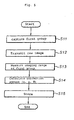
FIG. 4 is a flowchart showing an example of a procedure of a process that is performed by the image processing device according to the present invention. -
FIG. 5 is a flowchart showing an example of a position correction method as a pre-process included in the image process. -
FIG. 6 is a flowchart showing another example of a procedure of a process that is performed by the image processing device according to the present invention. -
Fig. 7 is a diagram showing an example of an inspection object that can be properly applied to the image processing device according to the present invention. -
FIG. 8 is a diagram showing another example of an inspection object that can be properly applied to the image processing device according to the present invention. -
FIG. 9 is a diagram showing an entire configuration of a related-art image processing device. -
FIG. 10 is a diagram for explaining a related-art image processing method. - Hereinafter, a preferred embodiment of the present invention will be described with reference to
FIGS. 1 to 8 . - As shown in
FIG. 1 , animage processing device 10 of the embodiment has general elements as described in the related art, that is, a CCD camera 11, an image processing device main body 12, a monitor 13, andcables cables inspection station 17 of aninspection line 16. An inspection object (substance) w flowing on theinspection line 16 at a predetermined tact temporarily stops in a defined location on theinspection station 17. In this state, an image of the inspection object W is captured by the camera 11. - As exemplarily shown in
FIG. 2 , a memory 13 of the image processing device main body 12 stores an imaging mode arbitrarily set by a user, specifically, an imaging range and an imaging condition. Whenever the image of the same inspection object is captured by the camera 11, the imaging mode of the CCD camera 11 can be changed according to the imaging mode stored in thememory 18. - A setup screen of the imaging mode exemplarily shown in
FIG. 2 will be described. The user can register the imaging modes of first to fourth groups Gr1 to Gr4 and can arbitrarily set the imaging range and the imaging condition of the camera for each group. The user may perform the setup work with the image processing device main body 12 or with an external apparatus connected to the image processing device main body 12, for example, a personal computer, while viewing the monitor 13. When the imaging range and the imaging condition are set by the external apparatus, the setup work may be performed during an image process by the image processing device main body 12. The imaging range and the imaging condition set in such a manner are stored in thememory 18. - When the image processing device main body 12 is provided with a section that sets the imaging range and the imaging condition, the image processing device main body 12 is preferably switchable between a setup mode that sets the imaging range and the imaging condition and an operation mode that captures an image through the camera and processes the captured image. The imaging mode registered by the user in the setup mode, that is, the imaging range and the imaging condition are stored in the
memory 18. In the operation mode, the imaging mode stored in thememory 18 is read and signals about the imaging range and the imaging condition read are supplied from the image processing device main body 12 to the CCD camera 11, such that the setup of the CCD camera 11 is performed. - More specifically, in the setup mode, the user assigns the imaging range and/or imaging condition through an assigning section (not shown) of the image processing device main body 12, and the imaging range and/or imaging condition assigned by the user is transmitted to the CCD camera 11. Then, a monitor display control section (not shown) of the image processing device main body 12 transmits the captured image of the assigned imaging range and/or imaging condition received from the CCD camera 11 to the monitor 13 and causes the monitor 13 to display the captured image of the assigned imaging range and/or imaging condition. The user can determine the imaging range and/or imaging condition while viewing the monitor 13 and the imaging range and/or imaging condition determined by the user is stored in the
memory 18. - The setup of the imaging mode will be described in detail with reference with
FIGS. 4 and5 . Referring toFIG. 2 , the imaging range 'UPPER LEFT' in the group Gr1 means that an upper left portion with respect to a CCDeffective pixel region 20 of the CCD camera 11 is registered as afirst imaging range 21a. Similarly, the imaging range 'UPPER RIGHT' in the group Gr2 means that an upper right portion with respect to the CCDeffective pixel region 20 is registered as asecond imaging range 21b. In the setup mode, when an arbitrary portion within the CCDeffective pixel region 20 is assigned as 'UPPER LEFT', 'UPPER RIGHT' or the like as described above, the range is preferably displayed on the monitor 13. Further, after confirming the range on the monitor , the user may allow the range to be stored in thememory 18. In such a registration method of the imaging range, preferably, the user may previously set the size of the imaging range. - Specifically, in an example of the registration shown in
FIG. 2 , based on the size of the imaging range 21 previously set and registered by the user, a location where the imaging range 21 is set is indicated and determined by selecting 'UPPER LEFT' or the like, such that the determined imaging range is stored in thememory 18. Further, among the imaging condition shown inFIG. 2 , for example, 'SHUTTER 1/500' represents a shutter speed. 'GAIN 5' or 'GAIN 6' represents the amplification factor of a CCD output signal. In the arrangement location setup of the imaging range 21, a coordinate X(+), Y(+) with an upper left corner as an origin may be indicated and registered. Further, for example, the shutter speed of the imaging condition changes brightness (exposure time). In addition, as registerable parameters as the imaging condition, that is, as the registerable imaging conditions, zoom (magnification), scanning modes, diaphragms, illumination or the like may be included. - The number of the groups Gr1 to Gr4 is not limited, and this is just an example. The first to fourth groups Gr1 to Gr4 correspond to the number of shutter times of (trigger number) with respect to one inspection object. The first group Gr1 substantially means a first trigger, that is, a first shutter with respect to the same inspection object, the second group Gr2 substantially means a second trigger, the third group Gr3 substantially means a third trigger, and the fourth group Gr4 substantially means a fourth trigger.
- An example of a procedure in which the camera 11 captures the image of the inspection object and the image processing device main body 12 receives and processes the captured image will be described with reference to a flowchart of
FIG. 4 . - If the inspection object W stops at a predetermined position on the
inspection station 17, the image processing device main body 12 synchronously receives a process start signal that is supplied from an exterior, such that the process is started. In a step S1, the imaging range and the imaging condition registered as the first group Gr1 are read from thememory 18, and the signals about the imaging range and the imaging condition of the first group Gr1 are supplied from the image processing device main body 12 to the CCD camera 11, such that the setup of the CCD camera 11 is performed. Then, the CCD camera 11 captures an image according to the imaging condition of the first group Gr1 (step S2). - In a next step S3, in the raw image captured by the CCD camera 11 (image of the entire view field region 20), the image (captured image) of the imaging range of the first group Gr1 is transmitted from the CCD camera 11 to the image processing device main body 12. In a step S4, the image processing device main body 12 receives the image (captured image) and performs the same image process as that in the related art.
- Here, the image process in the step S4 includes a position correction (x, y, θ) of an image about an x axis, a y axis, and a rotation θ, and further it means a process required for a desired inspection or measurement (for example, the size, the existence of defects, the number, the edge detection). The image process including the position correction is well-known, and thus the detailed description thereon will be omitted. As for the position correction, the procedure thereof will be described with reference to
FIG. 5 . After capturing the image with respect to the first group Gr1 in a step S11, the raw image is transmitted from the camera 11 to the image processing device main body 12 (step S12), and the measurement of the imaging range set on the first group is performed by the image processing device main body 12 (step S13). Then, the correction amount (x, y, θ) is calculated based on the measurement. The correction amount (x, y, θ) is stored in the memory of the image processing device main body 12. The correction amount (x, y, θ) is used for the pre-process (position correction) that is included in the image process of the second, third, or fourth group. - After the image of the first group Gr1 is captured and processed, the process returns to the step S1. Here, the imaging range and the imaging condition registered as the second group Gr2 are read from the
memory 18, and the signals about the imaging range and the imaging condition of the second group Gr2 are supplied from the image processing device main body 12 to the CCD camera 11, such that the setup of the CCD camera 11 is performed. Then, the CCD camera 11 captures an image according to the imaging condition of the second group Gr2 (the step S2). Subsequently, in the step S3, in the raw image captured by the CCD camera 11 (image of the entire view field region 20), the image (captured image) of the imaging range of the second group Gr2 is transmitted from the CCD camera 11 to the image processing device main body 12. In the step S4, the image processing device main body 12 receives the captured image and performs the same image process as that in the related art. - After the image of the second group Gr2 is captured and processed, the process returns to the step S1. Here, the imaging range and the imaging condition registered as the third group Gr3 are read from the
memory 18, and the signals about the imaging range and the imaging condition of the third group Gr3 are supplied from the image processing device main body 12 to the CCD camera 11, such that the setup of the CCD camera 11 is performed. Then, the CCD camera 11 captures an image according to the imaging condition of the third group Gr3 (the step S2). Subsequently, in the step S3, in the raw image captured by the CCD camera 11 (image of the entire view field region 20), the image (captured image) of the imaging range of the third group Gr3 is transmitted from the CCD camera 11 to the image processing device main body 12. In the step S4, the image processing device main body 12 receives the captured image and performs the same image process as that in the related art. - After the image of the third group Gr3 is captured and processed, the process returns to the step S1. Here, the imaging range and the imaging condition registered as the fourth group Gr4 are read from the
memory 18, and the signals about the imaging range and the imaging condition of the fourth group Gr4 are supplied from the image processing device main body 12 to the CCD camera 11, such that the setup of the CCD camera 11 is performed. Then, the CCD camera 11 captures an image according to the imaging condition of the fourth group Gr4 (the step S2). Subsequently, in the step S3, in the raw image captured by the CCD camera 11 (image of the entire view field region 20), the image (captured image) of the imaging range of the fourth group Gr4 is transmitted from the CCD camera 11 to the image processing device main body 12. In the step S4, the image processing device main body 12 receives the captured image and performs the same image process as that in the related art. - If the image of the fourth group Gr4 is captured and processed, in a step S5, it is judged that all groups are processed, and the inspection or measurement of the same inspection object is completed. Then, the
image processing device 10 waits until a next inspection object enters theinspection station 17. - For example, as seen from
FIG. 3 , as regards the image process of anoverlap portion 21c of imaging ranges 21a and 21b, when images captured several times are processed as one image, theoverlap portion 21c is needed to be processed. In this case, theoverlap portion 21c may be averaged to be processed. Further, the captured images may be respectively prioritized and the image process may be performed according to the priority. Alternatively, the captured images may be weighted and the image process may be performed according to the weight. - Further, when plural image processes (for example, from the image process of the first group Gr1 to subsequent image processes) are performed, the imaging range and the imaging condition in the current image process may be selectively changed according to the result of the previous image process. For example, when a tolerance inspection is performed with the image process of the first group Gr1, if the result falls within the tolerance (OK), the setup signals of the imaging range and the imaging condition are transmitted such that an area inspection of an additional location is performed, and the image is captured according to the setup signals of the imaging range and the imaging condition. To the contrary, if the result does not fall within the tolerance (NO), the setup signal for the change of the gain in the imaging range of the first group Gr1 is transmitted to the camera 11, and the image is captured according to the setup signals of the imaging range and the imaging condition, such that the imaging range of the first group Gr1 may be inspected again.
- As another example, for example, when a shape matching inspection is performed with the image process of the captured image under the first imaging range and imaging condition, if the shape matches with a first template, the tolerance inspection is subsequently performed with the same imaging range. Further, if the shape matches with a second template, a line defect inspection is subsequently performed with the same imaging range. If the shape does not match with the first or second template, a subsequent inspection may be changed according to the result of the image process such that the subsequent inspection may be not performed.
- Another example of a procedure in which the camera 11 captures the image of the inspection object and the image processing device main body 12 receives and processes the captured image will be described with reference to a flowchart of
FIG. 6 . - According to the procedure exemplarily shown in
FIG. 6 , the image of the imaging range 21 to be transmitted from the CCD camera 11 to the image processing device main body 12 for each group, that is, the captured image is stored in the image processing device main body 12, and, after the images of all groups are captured, the captured images of all groups are processed by the image processing device main body 12. - That is, the inspection object stops at a predetermined position, the image processing device main body 12 synchronously receives the process start signal that is supplied from the exterior, such that the process is started. First, in a step S21, the imaging range and the imaging condition registered as the first group Gr1 are read from the
memory 18, and the signals about the imaging range and the imaging condition of the first group Gr1 are supplied from the image processing device main body 12 to the CCD camera 11, such that the setup of the CCD camera 11 is performed. Then, the CCD camera 11 captures an image according to the imaging condition of the first group Gr1 (step S22). - In a next step S23, in the raw image captured by the CCD camera 11 (image of the entire view field 20), the image (captured image) of the
imaging range 21a of the first group Gr1 is supplied to the image processing device main body 12. The captured image is received by the image processing device main body 12. - After the image of the first group Gr1 is captured, the process returns to the step S21. Here, the imaging range and the imaging condition registered as the second group Gr2 are set on the CCD camera 11. Then, the CCD camera 11 captures an image according to the imaging range and the imaging condition of the second group Gr2 (the step S22). Subsequently, the image (captured image) of the
imaging range 21b of the second group Gr2 is supplied from the CCD camera 11 to the image processing device main body 12 (the step S23). - After the captured image of the second group Gr2 is received by the image processing device main body 12, the process returns to the step S21. Here, the imaging range and the imaging condition registered as the third group Gr3 are set on the CCD camera 11. Then, the CCD camera 11 captures an image according to the imaging condition of the third group Gr3 (the step S22). Subsequently, the image (captured image) of the
imaging range 21c of the third group Gr3 is supplied from the CCD camera 11 to the image processing device main body 12 (the step S23). - After the captured image of the third group Gr3 is received by the image processing device main body 12, the process returns to the step S21. Here, the imaging range and the imaging condition registered as the fourth group Gr4 are set on the CCD camera 11. Then, the CCD camera 11 captures an image according to the imaging condition of the fourth group Gr4 (the step S22). Subsequently, the image (captured image) of the imaging range 21d of the fourth group Gr4 is supplied from the CCD camera 11 to the image processing device main body 12 (the step S23).
- If the captured image of the fourth group Gr4 is received by the image processing device main body 12, in a step S24, it is judged that all groups are processed, and the process progresses to a step S25. In the step S25, the image processing device main body 12 processes the images of the respective groups. The image process includes the position correction (x, y, θ) of the image about the x axis, the y axis, and the rotation θ, and further it means the process required for the desired inspection or measurement (for example, the size, the existence of defects, the number, the edge detection). The image process including the position correction is well-known, and thus the detailed description thereon will be omitted.
- According to the procedure shown in
FIG. 6 , the captured images of the respective groups are received by and stored in the image processing device main body 12 and the image processing device main body 12 performs the image process after receiving the captured images of all groups. Thus, for the substance (inspection object) transferred to the inspection station at a short tact, the images can be synthesized while preventing blurring from being caused by the movement of the inspection object. In this case, however, the image processing device main body 12 requires the large memory space. - According to the
image processing device 10 of the embodiment, for example, as shown inFIG. 7 , for a substance 32 (inspection object) that hasregions respective regions respective regions respective regions - For example, when the
first region 30 is made of black resin and thesecond region 31 is made of a metal, a first portion surrounding thefirst region 30 is registered as the imaging range of the first group Gr1 and a portion surrounding thesecond region 31 is registered as the imaging range of the second group Gr2. Further, in the imaging range (the first region 30) registered as the first group Gr1, a relatively slow shutter speed may be registered such that the image does not become dark. Further, in the imaging range (the second region 31) registered as the second group Gr2, a relatively fast shutter speed may be registered such that the image does not have unduly high white levels. To the contrary, when a proper image about thefirst region 30 is captured, the illumination may become bright, and, when a proper image about thesecond region 31 is captured, the illumination may become dark, such that the reflection may be prevented. In this case, however, a sufficient response speed cannot be ensured due to the brightness control of the illumination. - Further, as exemplarily shown in
FIG. 8 , for example, asubstance 36 having apositioning mark 35 has the size to an extent that, if not reduced, it cannot be received by the image processing device main body 12. As regards such asubstance 36, a portion including thepositioning mark 35 that requires inspection precision is registered as afirst imaging range 21a, a proper magnification is set for capturing the image of the portion including themark 35, and the captured image of thefirst imaging range 21a is received by the image processing device main body 12. Further, a portion including aninspection object 37 in which inspection precision can be ensured with reduced scale is set to asecond imaging range 21b and a properly reduced magnification is set for the portion in which inspection precision can be ensured with reduced scale. The captured image of thesecond imaging range 21b may be received by the image processing device main body 12. - As described above, in the preferred embodiment of the present invention, the image processing device in which the CCD camera 11 and the image processing device main body 12 are connected to each other via the
cable 14 is described. Alternatively, the present invention can be properly applied to an image processing device in which the CCD camera 11 and the image processing device main body 12 are incorporated. Similarly, the present invention can be properly applied to an image processing device in which the image processing device main body 12 and the monitor 13 are incorporated. Further, the present invention can be properly applied to an image processing device in which the CCD camera 11, the image processing device 12, and the monitor 13 are incorporated. - Further, the setup of the imaging range and/or imaging condition of the CCD camera 11 may be performed by the signal from the external apparatus. The setup by the signal from the external apparatus may be performed during the image process by the image processing device main body 12.
- Further, as a solid-state image element of a camera which can be applied to the present invention, instead of the CCD, a CMOS image sensor may be adapted. In the case of the CMOS image sensor, the advantages according to the present invention can be obtained.
- It will be apparent to those skilled in the art that various modifications and variations can be made to the described preferred embodiments of the present invention without departing from the spirit or scope of the invention. Thus, it is intended that the present invention cover all modifications and variations of this invention consistent with the scope of the appended claims and their equivalents.
Claims (11)
- An image processing device (10) comprising:a solid-state image element camera (11) that captures a raw image of an inspection object corresponding to an entire view field region of the solid-state image element camera having an imaging range of the solid-state image element camera, wherein the imaging range (21a, 21b) is a portion of the entire view field region (20) and is adapted to be arbitrarily set within the entire view field region (20);an image processing device main body (12) that receives and processes the captured image from the camera; anda monitor (13) that displays an inspection or measurement result by the image processing device main body,the image processing device main body (12) comprises a storing section, a transmitting section, an assigning section and a receiving section; wherein the assigning section assigns the imaging range on behalf of a user, wherein the storing section (18) is adapted to store the imaging range (21 a, 21 b) assigned by the user; wherein the transmitting section is adapted for reading the imaging range stored in the storing section and transmitting a signal about the read imaging range from the image processing device main body to the solid-state image element camera; and wherein the receiving section of the image processing device main body (12) is adapted to receive a captured image signal corresponding to the imaging range from the solid-state image element camera;wherein the image processing device performs an image process based on the captured image signal received by the receiving section.
- The image processing device according to claim 1,
wherein the imaging range (21a, 21 b, 21 c) of the solid-state image element camera (11) is set by an external apparatus connected to the image processing device main body. - The image processing device according to claim 1 or 2
wherein the imaging range (21a, 21b, 21c) of the solid-state image element camera (11) is set by the external apparatus during the image process by the image processing device main body. - The image processing device according to any one of the claims 1 to 3
wherein the storing section (18) further stores an imaging condition set by the user, and
the image processing device main body (12) reads the imaging condition from the storing section, together with the imaging range, transmits signals about the imaging range and the imaging condition to the solid-state image element camera, and sets the imaging condition on the solid-state image element camera to capture an image. - The image processing device according to claim 4,
wherein the imaging condition is at least one selected from a group of magnification and scanning modes of the solid-state image element camera, an amplification factor of an output signal of the solid-state image element camera, and a shutter speed, diaphragms and illumination of the solid-state image element camera. - The image processing device according to any one of the claims 1 to 5
wherein the solid-state image element camera (11) and the image processing device main body (12) are connected to each other via a cable (14). - The image processing device according to any one of the claims 1 to 6
wherein the image processing device main body (12) has:an assigning section that assigns the imaging range on behalf of the user;the transmitting section that transmits the imaging range assigned by the assigning section to the solid-state image element camera;the receiving section that receives the signal about the captured image of the assigned imaging range from the solid-state image element camera;a monitor display control section that transmits the captured image received from the solid-state image element camera to the monitor and causes the monitor to display the captured image; andthe storing section that stores the imaging range determined by the user. - The image processing device according to any one of the claims 1 to 7
wherein the image processing device main body (12) has: an assigning section that assigns the imaging range and the imaging condition on behalf of the user;
the transmitting section that transmits the imaging range and the imaging condition assigned by the assigning section to the solid-state image element camera;
the receiving section that receives the signal about the captured image of the assigned imaging range captured under the assigned imaging condition from the solid-state image element camera;
a monitor display control section that transmits the captured image received from the solid-state image element camera to the monitor and causes the monitor to display the captured image; and
the storing section that stores the imaging range and imaging condition determined by the user. - An image processing method performed in an image processing device, comprising:assigning an imaging range of a solid-state image element camera on behalf of a user,storing the imaging range assigned by the user wherein the imaging range (21a, 21b) is a portion of the entire view field region (20) and is adapted to be arbitrarily set within the entire view field region (20);capturing a raw image of an inspection object by the solid-state image element camera corresponding to the entire view field region and generating a captured image signal corresponding to the stored imaging range in the image captured by the solid-state image element camera;receiving from the solid-state image element camera (11) the captured image signal in the image processing device main body (12); andperforming an image process based on the captured image signal generated.
- The image processing method according to claim 9, further comprising:assigning the imaging range on behalf of the user;capturing an image of an inspection object by the solid-state image element camera and generating a captured image of the assigned imaging range in the image captured by the solid-state image element camera; anddisplaying the captured image of the assigned imaging range received from the solid-state image element camera; andstoring the imaging range determined by the user as the set imaging range of the solid-state image element camera.
- The image processing method according to claim 9, further comprising:setting the imaging range of the solid-state image element camera by an external apparatus connected to the image processing device.
Applications Claiming Priority (2)
| Application Number | Priority Date | Filing Date | Title |
|---|---|---|---|
| JP2004034514 | 2004-02-12 | ||
| JP2004034514A JP4521858B2 (en) | 2004-02-12 | 2004-02-12 | Image processing device |
Publications (3)
| Publication Number | Publication Date |
|---|---|
| EP1564547A2 EP1564547A2 (en) | 2005-08-17 |
| EP1564547A3 EP1564547A3 (en) | 2005-09-14 |
| EP1564547B1 true EP1564547B1 (en) | 2010-10-27 |
Family
ID=34697897
Family Applications (1)
| Application Number | Title | Priority Date | Filing Date |
|---|---|---|---|
| EP05003046A Expired - Lifetime EP1564547B1 (en) | 2004-02-12 | 2005-02-14 | Image processing device and image processing method |
Country Status (5)
| Country | Link |
|---|---|
| US (1) | US7982779B2 (en) |
| EP (1) | EP1564547B1 (en) |
| JP (1) | JP4521858B2 (en) |
| CN (1) | CN100593104C (en) |
| DE (1) | DE602005024330D1 (en) |
Families Citing this family (9)
| Publication number | Priority date | Publication date | Assignee | Title |
|---|---|---|---|---|
| US7999861B2 (en) * | 2008-03-14 | 2011-08-16 | Omron Corporation | Image processing apparatus for generating composite image with luminance range optimized for a designated area |
| JP2010278510A (en) * | 2009-05-26 | 2010-12-09 | Elmo Co Ltd | Document presentation device |
| CN101929837B (en) * | 2009-06-22 | 2012-06-27 | 牧德科技股份有限公司 | Quadratic element optical measuring device capable of continuously conveying objects to be measured |
| JP5841427B2 (en) | 2011-12-28 | 2016-01-13 | 株式会社キーエンス | Image processing apparatus and image processing method |
| JP5890692B2 (en) * | 2012-01-13 | 2016-03-22 | キヤノン株式会社 | Imaging apparatus, control method, and program |
| JP6474334B2 (en) * | 2015-07-30 | 2019-02-27 | 株式会社キーエンス | Image inspection apparatus, image inspection method, and image inspection program |
| JP6333871B2 (en) * | 2016-02-25 | 2018-05-30 | ファナック株式会社 | Image processing apparatus for displaying an object detected from an input image |
| JP6917762B2 (en) * | 2017-05-09 | 2021-08-11 | 株式会社キーエンス | Image inspection equipment |
| CN109613001B (en) * | 2018-11-07 | 2021-02-19 | 常州信息职业技术学院 | A signal receiving and processing device based on visual communication |
Family Cites Families (25)
| Publication number | Priority date | Publication date | Assignee | Title |
|---|---|---|---|---|
| JPS60236592A (en) * | 1984-05-10 | 1985-11-25 | Toppan Printing Co Ltd | Inspection device of omitted printing of printed matter |
| US5262871A (en) * | 1989-11-13 | 1993-11-16 | Rutgers, The State University | Multiple resolution image sensor |
| JP3007392B2 (en) * | 1990-08-16 | 2000-02-07 | ニチデン機械株式会社 | Pattern recognition method and apparatus |
| CA2218563A1 (en) * | 1996-10-18 | 1998-04-18 | Consolidated Papers, Inc. | Method of and system for video surveillance of a fast moving web |
| JP3759280B2 (en) * | 1997-04-15 | 2006-03-22 | 富士通株式会社 | Event detection device for road monitoring |
| JPH117392A (en) | 1997-06-17 | 1999-01-12 | Tec Corp | Data processor obtained by duplexing auxiliary storage device and method for falling system of data processor |
| US6670991B1 (en) * | 1997-09-26 | 2003-12-30 | Canon Kabushiki Kaisha | Image sensing system, control method, and recording medium for controlling a camera apparatus utilizing a client device connected thereto |
| JPH11103410A (en) * | 1997-09-26 | 1999-04-13 | Canon Inc | Camera control system, control method therefor, and storage medium storing program for executing the processing |
| JPH11133292A (en) * | 1997-10-28 | 1999-05-21 | Canon Inc | Imaging system, control method therefor, and storage medium storing program for executing the processing |
| JPH11122540A (en) | 1997-10-17 | 1999-04-30 | Hamamatsu Photonics Kk | Ccd camera, controller for ccd camera and sensitivity adjustment method for ccd camera |
| US6047042A (en) | 1998-03-25 | 2000-04-04 | Continental X-Ray Corporation | Automatic exposure and brightness control for fluoroscopic and radio-graphic imaging |
| US7161619B1 (en) * | 1998-07-28 | 2007-01-09 | Canon Kabushiki Kaisha | Data communication system, data communication control method and electronic apparatus |
| JP2000138870A (en) * | 1998-10-30 | 2000-05-16 | Canon Inc | Data communication system, terminal device, system control method, and storage medium |
| JP4124866B2 (en) * | 1998-07-28 | 2008-07-23 | キヤノン株式会社 | Image communication system and control apparatus |
| JP4227238B2 (en) | 1999-02-19 | 2009-02-18 | 株式会社キーエンス | Image display method, image processing apparatus, and recording medium |
| JP2000329536A (en) * | 1999-05-19 | 2000-11-30 | Nec Corp | Apparatus and method for visual inspection |
| KR100374046B1 (en) * | 1999-09-30 | 2003-03-03 | 오므론 가부시키가이샤 | Image Processing Apparatus, Image Processing Method and Visual Inspection System |
| US6920241B1 (en) * | 2000-09-29 | 2005-07-19 | Cognex Corporation | System and method for bundled location and regional inspection |
| JP2002230546A (en) | 2001-01-30 | 2002-08-16 | Fujitsu Ltd | Image processing program, computer-readable recording medium storing image processing program, image processing method, and image processing apparatus |
| JP4014379B2 (en) * | 2001-02-21 | 2007-11-28 | 株式会社日立製作所 | Defect review apparatus and method |
| JP2003098112A (en) * | 2001-09-25 | 2003-04-03 | Hitachi Ltd | Method and apparatus for detecting and outputting surface image of thin film device, method of manufacturing thin film device using the same, and apparatus for manufacturing the same |
| JP4726367B2 (en) | 2001-09-28 | 2011-07-20 | 株式会社キーエンス | Image processing area designation circuit, image processing area designation method, image processing area designation program, and computer-readable recording medium |
| US20030185432A1 (en) * | 2002-03-29 | 2003-10-02 | Hong Dezhong | Method and system for image registration based on hierarchical object modeling |
| JP4275378B2 (en) | 2002-09-27 | 2009-06-10 | 富士重工業株式会社 | Stereo image processing apparatus and stereo image processing method |
| US20050117017A1 (en) * | 2003-12-01 | 2005-06-02 | Baer Richard L. | System and method for imaging regions of interest |
-
2004
- 2004-02-12 JP JP2004034514A patent/JP4521858B2/en not_active Expired - Fee Related
-
2005
- 2005-02-10 US US11/055,270 patent/US7982779B2/en not_active Expired - Fee Related
- 2005-02-14 DE DE602005024330T patent/DE602005024330D1/en not_active Expired - Lifetime
- 2005-02-14 EP EP05003046A patent/EP1564547B1/en not_active Expired - Lifetime
- 2005-02-16 CN CN200510069768A patent/CN100593104C/en not_active Expired - Fee Related
Also Published As
| Publication number | Publication date |
|---|---|
| JP4521858B2 (en) | 2010-08-11 |
| EP1564547A2 (en) | 2005-08-17 |
| US20050178949A1 (en) | 2005-08-18 |
| CN100593104C (en) | 2010-03-03 |
| EP1564547A3 (en) | 2005-09-14 |
| CN1755321A (en) | 2006-04-05 |
| JP2005227931A (en) | 2005-08-25 |
| DE602005024330D1 (en) | 2010-12-09 |
| US7982779B2 (en) | 2011-07-19 |
Similar Documents
| Publication | Publication Date | Title |
|---|---|---|
| KR100399884B1 (en) | Apparatus and method for defective pixel concealment of image sensor | |
| US20100295932A1 (en) | Image obtaining apparatus, image synthesis method and microscope system | |
| CN103139492B (en) | Camera head, image capture method and the system of supervision | |
| CN102469258B (en) | Image processor, method of controlling the same | |
| JPWO2011055468A1 (en) | Imaging apparatus, adjustment apparatus, and optical axis adjustment system for imaging apparatus | |
| JP4453332B2 (en) | Defective pixel detection method, detection apparatus, and imaging apparatus | |
| US7936948B2 (en) | System and method for merging differently focused images | |
| US7982779B2 (en) | Image processing device and image processing method | |
| JP2011077825A (en) | Display device, display system, display method and program | |
| JP3696069B2 (en) | Method and apparatus for detecting defective pixels of solid-state image sensor | |
| JPH08254499A (en) | Display / appearance inspection device | |
| US20090033774A1 (en) | Imaging device | |
| JP2005210164A5 (en) | ||
| CN101267502A (en) | Imaging apparatus and image data recording method | |
| JP2001045359A (en) | Hand shake correcting method for solid-state image pickup device, and solid-state image pickup device | |
| JP2014007599A (en) | Image pick-up device, defect processing method, defect processing program and electronic information apparatus | |
| JP2005175719A (en) | Imaging apparatus and imaging system | |
| JP3615463B2 (en) | Digital camera and inspection device | |
| JPH02264561A (en) | Adjusting method for optical unit of image pickup element | |
| JPH0548977A (en) | Telecamera | |
| KR100278670B1 (en) | Inspection method and apparatus for TV screen | |
| JP2004112268A (en) | Camera adjustment inspection device | |
| JP2008131109A (en) | IMAGING DEVICE AND IMAGING DEVICE CONTROL METHOD | |
| JP2002051261A (en) | Image reading apparatus and image reading method | |
| US20100026861A1 (en) | Image capture device and image processing method for the same |
Legal Events
| Date | Code | Title | Description |
|---|---|---|---|
| PUAI | Public reference made under article 153(3) epc to a published international application that has entered the european phase |
Free format text: ORIGINAL CODE: 0009012 |
|
| PUAL | Search report despatched |
Free format text: ORIGINAL CODE: 0009013 |
|
| AK | Designated contracting states |
Kind code of ref document: A2 Designated state(s): AT BE BG CH CY CZ DE DK EE ES FI FR GB GR HU IE IS IT LI LT LU MC NL PL PT RO SE SI SK TR |
|
| AX | Request for extension of the european patent |
Extension state: AL BA HR LV MK YU |
|
| AK | Designated contracting states |
Kind code of ref document: A3 Designated state(s): AT BE BG CH CY CZ DE DK EE ES FI FR GB GR HU IE IS IT LI LT LU MC NL PL PT RO SE SI SK TR |
|
| AX | Request for extension of the european patent |
Extension state: AL BA HR LV MK YU |
|
| 17P | Request for examination filed |
Effective date: 20060207 |
|
| AKX | Designation fees paid |
Designated state(s): DE GB |
|
| 17Q | First examination report despatched |
Effective date: 20070212 |
|
| GRAP | Despatch of communication of intention to grant a patent |
Free format text: ORIGINAL CODE: EPIDOSNIGR1 |
|
| RTI1 | Title (correction) |
Free format text: IMAGE PROCESSING DEVICE AND IMAGE PROCESSING METHOD |
|
| GRAS | Grant fee paid |
Free format text: ORIGINAL CODE: EPIDOSNIGR3 |
|
| GRAA | (expected) grant |
Free format text: ORIGINAL CODE: 0009210 |
|
| AK | Designated contracting states |
Kind code of ref document: B1 Designated state(s): DE GB |
|
| REG | Reference to a national code |
Ref country code: GB Ref legal event code: FG4D |
|
| REF | Corresponds to: |
Ref document number: 602005024330 Country of ref document: DE Date of ref document: 20101209 Kind code of ref document: P |
|
| PLBE | No opposition filed within time limit |
Free format text: ORIGINAL CODE: 0009261 |
|
| STAA | Information on the status of an ep patent application or granted ep patent |
Free format text: STATUS: NO OPPOSITION FILED WITHIN TIME LIMIT |
|
| 26N | No opposition filed |
Effective date: 20110728 |
|
| REG | Reference to a national code |
Ref country code: DE Ref legal event code: R097 Ref document number: 602005024330 Country of ref document: DE Effective date: 20110728 |
|
| PGFP | Annual fee paid to national office [announced via postgrant information from national office to epo] |
Ref country code: DE Payment date: 20120208 Year of fee payment: 8 |
|
| PGFP | Annual fee paid to national office [announced via postgrant information from national office to epo] |
Ref country code: GB Payment date: 20120208 Year of fee payment: 8 |
|
| GBPC | Gb: european patent ceased through non-payment of renewal fee |
Effective date: 20130214 |
|
| REG | Reference to a national code |
Ref country code: DE Ref legal event code: R119 Ref document number: 602005024330 Country of ref document: DE Effective date: 20130903 |
|
| PG25 | Lapsed in a contracting state [announced via postgrant information from national office to epo] |
Ref country code: GB Free format text: LAPSE BECAUSE OF NON-PAYMENT OF DUE FEES Effective date: 20130214 Ref country code: DE Free format text: LAPSE BECAUSE OF NON-PAYMENT OF DUE FEES Effective date: 20130903 |