EP1562289A2 - Electronic part and method of manufacturing the same - Google Patents
Electronic part and method of manufacturing the same Download PDFInfo
- Publication number
- EP1562289A2 EP1562289A2 EP05002294A EP05002294A EP1562289A2 EP 1562289 A2 EP1562289 A2 EP 1562289A2 EP 05002294 A EP05002294 A EP 05002294A EP 05002294 A EP05002294 A EP 05002294A EP 1562289 A2 EP1562289 A2 EP 1562289A2
- Authority
- EP
- European Patent Office
- Prior art keywords
- substrate
- case body
- seal material
- electronic part
- metal film
- Prior art date
- Legal status (The legal status is an assumption and is not a legal conclusion. Google has not performed a legal analysis and makes no representation as to the accuracy of the status listed.)
- Withdrawn
Links
Images




Classifications
-
- H—ELECTRICITY
- H03—ELECTRONIC CIRCUITRY
- H03H—IMPEDANCE NETWORKS, e.g. RESONANT CIRCUITS; RESONATORS
- H03H9/00—Networks comprising electromechanical or electro-acoustic elements; Electromechanical resonators
- H03H9/02—Details
- H03H9/05—Holders or supports
- H03H9/10—Mounting in enclosures
- H03H9/1064—Mounting in enclosures for surface acoustic wave [SAW] devices
- H03H9/1078—Mounting in enclosures for surface acoustic wave [SAW] devices the enclosure being defined by a foil covering the non-active sides of the SAW device
-
- H—ELECTRICITY
- H03—ELECTRONIC CIRCUITRY
- H03H—IMPEDANCE NETWORKS, e.g. RESONANT CIRCUITS; RESONATORS
- H03H3/00—Apparatus or processes specially adapted for the manufacture of impedance networks, resonating circuits, resonators
- H03H3/007—Apparatus or processes specially adapted for the manufacture of impedance networks, resonating circuits, resonators for the manufacture of electromechanical resonators or networks
- H03H3/08—Apparatus or processes specially adapted for the manufacture of impedance networks, resonating circuits, resonators for the manufacture of electromechanical resonators or networks for the manufacture of resonators or networks using surface acoustic waves
-
- H—ELECTRICITY
- H03—ELECTRONIC CIRCUITRY
- H03H—IMPEDANCE NETWORKS, e.g. RESONANT CIRCUITS; RESONATORS
- H03H9/00—Networks comprising electromechanical or electro-acoustic elements; Electromechanical resonators
- H03H9/02—Details
- H03H9/05—Holders or supports
- H03H9/10—Mounting in enclosures
- H03H9/1064—Mounting in enclosures for surface acoustic wave [SAW] devices
- H03H9/1085—Mounting in enclosures for surface acoustic wave [SAW] devices the enclosure being defined by a non-uniform sealing mass covering the non-active sides of the SAW device
-
- H—ELECTRICITY
- H03—ELECTRONIC CIRCUITRY
- H03H—IMPEDANCE NETWORKS, e.g. RESONANT CIRCUITS; RESONATORS
- H03H9/00—Networks comprising electromechanical or electro-acoustic elements; Electromechanical resonators
- H03H9/02—Details
- H03H9/02535—Details of surface acoustic wave devices
- H03H9/02818—Means for compensation or elimination of undesirable effects
- H03H9/02913—Measures for shielding against electromagnetic fields
-
- H—ELECTRICITY
- H10—SEMICONDUCTOR DEVICES; ELECTRIC SOLID-STATE DEVICES NOT OTHERWISE PROVIDED FOR
- H10W—GENERIC PACKAGES, INTERCONNECTIONS, CONNECTORS OR OTHER CONSTRUCTIONAL DETAILS OF DEVICES COVERED BY CLASS H10
- H10W72/00—Interconnections or connectors in packages
- H10W72/851—Dispositions of multiple connectors or interconnections
- H10W72/874—On different surfaces
- H10W72/877—Bump connectors and die-attach connectors
-
- H—ELECTRICITY
- H10—SEMICONDUCTOR DEVICES; ELECTRIC SOLID-STATE DEVICES NOT OTHERWISE PROVIDED FOR
- H10W—GENERIC PACKAGES, INTERCONNECTIONS, CONNECTORS OR OTHER CONSTRUCTIONAL DETAILS OF DEVICES COVERED BY CLASS H10
- H10W90/00—Package configurations
- H10W90/701—Package configurations characterised by the relative positions of pads or connectors relative to package parts
- H10W90/721—Package configurations characterised by the relative positions of pads or connectors relative to package parts of bump connectors
- H10W90/724—Package configurations characterised by the relative positions of pads or connectors relative to package parts of bump connectors between a chip and a stacked insulating package substrate, interposer or RDL
Definitions
- the present invention relates to an electronic part in which an electronic element is sealed in a case body and a method of manufacturing the same, and more particularly to an electronic part having a miniaturized case body and a method of manufacturing the same.
- Figs. 17 and 18 are cross sectional views showing the structure that a surface acoustic element is sealed in a concave portion provided in a case body made of ceramic.
- the structure of Fig. 17 is described in Japanese unexamined Patent Application Publication No. 2001-77659 and the structure of Fig. 18 is described in Japanese unexamined Patent Application Publication No. 2003-87093.
- a case body 3 of an electric part shown in Fig. 17 is formed with the concave portion, and an accommodating portion 5 in which an electronic element 1 is accommodated by the concave portion is formed.
- the electronic element 1 is accommodated in the accommodating portion 5 and the electronic element 1 is mounted in the accommodating portion 5 on the case body 3.
- the electronic element 1 is formed with a terminal (not shown) and the terminal is electrically connected to a connecting land 2 formed in the accommodating portion 5.
- the electronic element 1 is, for example, a band pass filter formed by using the surface acoustic element.
- the surface acoustic element has a structure that teeth portions of a pair of teeth-shaped electrodes (IDT (inter-digital transducer) electrodes) which is made of a conductive material having a low specific gravity are differently arranged on the surface of a piezoelectric substrate.
- IDT inter-digital transducer
- the surface acoustic element having such a simple structure is a suitable element to miniature a filter, a resonator or a duplexer mounted in mobile communication terminals.
- the upper side of the accommodating portion 5 is an open surface, and a cover body 4 made of a metal is formed so as to close the open surface.
- a cover body 4 made of a metal is formed so as to close the open surface.
- the electronic part shown in Fig. 18 is provided with a conductive resin 6 between the electronic element 1 and the cover body 4, and thereby the Joule heat generated from the electronic element 1 is easily emitted to the outside.
- an upper surface 3a of the case body 3 in order to seal the electronic element 1 in the accommodating portion 5, an upper surface 3a of the case body 3 must be positioned at a height higher than a bottom surface 1a of the electronic element 1, thereby generating a gap s1 between the cover body 4 and the bottom surface 1a of the electronic element 1. On this account, it is difficult to make an electronic part thin. Also, in the electronic part shown in Fig. 18, similarly, a gap s2 is formed between the cover body 4 and the electronic element 1.
- the present invention is designed to solve the above-mentioned problems, and it is an object of the present invention is to provide an electronic part and a method of manufacturing the same, in which the electronic part can be made thin by reducing or eliminating a gap between a cover body and an electronic element.
- the electronic part according to the present invention comprises a substrate on which an electronic element is mounted or is formed and a case body having an accommodating part for accommodating the substrate, wherein the substrate is accommodated in the accommodating portion so that the surface thereof is opposed to a bottom surface of the accommodating portion, and resin seal material is provided over a range from the bottom surface of the substrate to the sidewall portion around the accommodating portion of the case body, and a metal film is laminated on the seal material.
- the resin seal material is provided over a range from the bottom surface of the substrate to the sidewall portion around the accommodating portion of the case body and the metal film is laminated on the seal material, the height difference between an upper surface of the sidewall portion of the case body and a bottom surface of the electronic element can be reduced, thereby the electronic part can be made thin.
- a gap between the cover body and the electronic element is removed, thereby the electronic part can be further made thin.
- the seal material may have a uniform thickness throughout an overall area of a bottom surface of the substrate. Also, when a surface of the seal material on a bottom surface of the substrate is formed with irregularities, the surface area of the seal material is increased and thus the emitting effect of the Joule heat generated from the electronic part is increased.
- the seal material is formed over a range from a peripheral portion of the bottom surface of the substrate to a sidewall portion of the case body, and a through-hole is formed in the seal material on an inside of a bottom surface of the substrate, thereby the area that the metal film is directly laminated on the substrate is provided.
- the emitting effect of the Joule heat generated from the electronic element is further increased.
- the surface of the metal film is formed with irregularities on a bottom surface of the substrate.
- the metal film is electrically connected to a connecting portion provided on a lower surface of the case body through a conductive portion provided at an outside or inside of the bottom portion of the case body and at an outside or inside of the sidewall portion of the case body, thereby increasing the shield effect.
- the conductive portion is formed inside a groove portion provided at an outside of the sidewall portion of the case body, and a lower end of the groove portion is positioned inside the sidewall portion of the case body so that the bottom of the case body is not exposed. If a lower end of the groove portion is not exposed to a bottom surface of the case body, the solder can be prevented from being sucked into the groove portion when soldering the electronic part on the wiring substrate.
- the method of manufacturing an electronic part comprises the steps of: (a) forming a concave portion in a case body to provide an accommodating portion; (b) accommodating a substrate on which an electronic element is mounted or formed in the accommodating portion so that the surface of the substrate is opposed to a bottom surface of the accommodating portion, thereby the bottom surface of the substrate is directed upward; (c) providing a resin seal material over a range from the bottom surface of the substrate to a sidewall portion around the accommodating portion of the case body; and (d) laminating a metal film on the seal material.
- the substrate is arranged so that the bottom surface of the substrate is positioned at the same virtual plane of an upper surface of the sidewall portion of the case body, or the substrate is arranged so that the bottom surface of the substrate is positioned at a height higher than an upper surface of the sidewall portion of the case body.
- the seal material has a uniform thickness throughout an overall area of a bottom surface of the substrate. Also, it is more preferable that the surface of the seal material on a bottom surface of the substrate may be formed with irregularities.
- step (c) a through-hole is formed in the seal material on an inside of the bottom surface of the substrate, and, in step (d), the metal film is directly laminated on the substrate exposed to the through-hole.
- step (d) the metal film is formed so that the surface thereof has the irregularities on the bottom surface of the substrate.
- a method for electrically connecting the metal film to the connecting portion provided on a bottom surface of the case body through the conductive portion provided at an outside or inside of the bottom portion of the case body or at an outside or inside of the sidewall portion of the case body to increase the shield effect there is a method which further comprises, before step (a), a step (e) of forming a connecting portion electrically connected to the electronic element and a connecting portion electrically connected to the metal film, on a bottom surface of the case body, before step (a) or the step (b), a step (f) of forming a conductive portion electrically connected to the connecting portion of a bottom surface of the case body at an outside or inside of the sidewall portion of the case body, wherein, in step (c), the seal material on the conductive portion is removed after covering the conductive portion by the seal material, and in step (d), the metal film and the conductive
- the height difference between an upper surface of the sidewall portion of the case body and the bottom surface of the electronic part can be reduced, thereby thinning the electronic part.
- a bottom surface of the substrate is positioned on the same virtual plane of an upper surface of the sidewall portion of the case body, or the bottom surface of the substrate is positioned at a height higher than the upper surface of the sidewall portion of the case body, the gap between the cover body and the electronic element can be removed, thereby further thinning the electronic part.
- a metal film is electrically connected to a connecting portion provided on a lower surface of the case body through a conductive portion provided at an outside or inside of the bottom portion of the case body and at an outside or inside of the sidewall portion of the case body, the shield effect is increased.
- Fig. 1 is a cross sectional view of an electronic part according to a first embodiment of the present invention.
- the electronic part shown in Fig. 1 is formed by sealing a surface acoustic element in a concave portion provided in a case body made of ceramic.
- a concave portion is formed by providing a sidewall portion 13b on the bottom portion 13a.
- an accommodating portion 15 for accommodating an electronic element 11 is formed.
- the substrate 11c of the electronic element 11 is accommodated in the accommodating portion 15 so that the surface 11d thereof is opposed to a bottom surface 15a of the accommodating portion 15, and thus the bottom surface 11b of the substrate 11c is directed upward.
- the electronic element 11 is formed with terminals 11a, 11a, and the terminals 11a, 11a are electrically connected to connecting lands 12, 12 formed in the accommodating portion 15.
- the lands 12, 12 are electrically connected to the connecting portions 21, 21 provided on a lower surface of the bottom portion 13a through conducting portions 20, 20 passing through the bottom portion 13a of the case body 13.
- the electronic element 11 is, for example, a band pass filter formed by using a surface acoustic element.
- the surface acoustic element has the structure that the teeth portions of a pair of teeth-shaped electrodes (IDT (inter-digital transducer) electrodes) which is made of conductive material having a low specific gravity are differently arranged on the surface of a piezoelectric substrate.
- IDT inter-digital transducer
- the surface acoustic element having such a simple structure is the suitable element to miniature a filter, a resonator or a duplexer mounted in a mobile communication terminal.
- the upper side of the accommodating portion 15 is an open surface and, in order to close the open surface, seal material 16 made of resin is provided over a range from the bottom surface 11b of the substrate 11c of the electronic element 11 to the sidewall portion 13b around the accommodating portion 15 of the case body 13.
- a metal film 17 is laminated on the seal material'16.
- the seal material 16 is formed by thermosetting resin such as epoxy resin or polyimide resin. Particularly, it is preferable that epoxy resin having low water permeability is used.
- the bottom surface 11b of the substrate 11c of the electronic element 11 is positioned on the same virtual plane A of an upper surface 13b1 of the sidewall portion 13b of the case body 13. Accordingly, the gap is not formed between the seal material 16 and the bottom surface 11b of the electronic element 11, thereby it becomes.easier to make the electronic part thin. Also, since the seal material 16 is made of resin, even when the positions of the bottom surface 11b of the substrate 11c and an upper surface 13b1 of the sidewall portion 13b are deviated, the deviation can be easily absorbed.
- the bottom surface 11b of the substrate 11c of the electronic element 11 may be positioned at a height higher than an upper surface 13b1 of the sidewall portion 13b of the case body 13.
- the seal material 16 has a uniform thickness throughout an overall area of the bottom surface 11b of the substrate 11c. There is a case that the seal material 16 is slightly drooped downward between the bottom surface 11b of the substrate 11c and the sidewall portion.
- a conductive portion 22 and a conductive portion 23 composed of conductive material are provided at an outside and inside of the sidewall portion 13 of the case body 13 of the electronic part E1.
- a connecting portion 25 is provided at a bottom surface of the case body 13 and the conductive portion 24 passing through the bottom portion 13a of the case body 13.
- the conductive portions 22, 23, 24 and the connecting portion 25 are electrically connected, and the connecting portion 25 is grounded.
- the conductive portion 22 connected to the metal film 17 is formed inside a groove portion 30 provided at an outside of the sidewall portion 13b of the case body 13.
- a lower end 30a of the groove portion 30 is positioned inside the sidewall portion 13b of the case body 13 so as not to be exposed to a bottom surface 13a1 of the case body 13. Thereby, the solder can be prevented from being sucked into the groove portion 30 when soldering the electronic part E1 on the wiring substrate.
- Fig. 1 is a cross sectional view when the electronic part cut along the line 1-1 in Fig. 2 is seen from the arrow direction.
- Fig. 3 is a cross sectional view of the electronic part E2 according to a second embodiment of the present invention.
- the electronic part E2 shown in Fig. 3 is different from the electronic part E1 shown in Fig. 1 only in that a conductive portion 40 and a conductive portion 41 composed of conductive material are provided inside the sidewall portion 13b of the case body 13.
- the conductive portions 40, 41, 42 and the connecting portion 25 are electrically connected and the connecting portion 25 is grounded.
- Figs. 4 and 5 are cross sectional views of electronic parts according to third and fourth embodiments of the present invention, respectively.
- a seal material 51 is formed over a range from a peripheral portion 11b1 of the bottom surface 11b of the substrate 11c of the electronic element 11 to the case body 13b, a through-hole 51a is formed in the seal material 51 on an inside portion 11b2 of the bottom surface 11b of the substrate 11c, thereby the area that the metal film 50 is directly laminated on the substrate 11c is provided. If the metal film 50 is directly laminated on the substrate 11c, the emitting effect of the Joule heat generated from the electronic element 11 becomes increased.
- the surface of the metal film 50 is formed with irregularities composed of a concave portion 50a and a convex portion 50b on the bottom surface 11b of the substrate 11c, thereby increasing the surface area and thus further increasing the emitting effect of the Joule heat.
- the electronic part E4 shown in Fig. 5 is similar to the electronic part E3 shown in Fig. 4 and is different from it in that, on an inside portion 11b2 of the bottom surface 11b of the substrate 11c, a plurality of through-holes are formed in the seal material 52 and a metal film 53 is directly laminated on the substrate 11c in the through-hole.
- the surface of the metal film 53 is formed with irregularities composed of a concave portion 53b and a convex portion 53a on the bottom surface 11b of the substrate 11c.
- the electronic part E4 shown in Fig. 5 has the same effect as the electronic part E3 shown in Fig. 4.
- the electronic parts E3, E4 shown in Figs. 4 and 5 does not need the expensive conductive resin 6 between the electronic element 1 and the cover body 4, unlike the conventional electronic part shown in Fig. 18, and thus the structure for efficiently emitting the Joule heat generated from the electronic element 11 to an outside thereof can be realized with a low cost.
- the electronic part E5 shown in Fig. 6 is similar to the electronic part E3 shown in Fig. 4 and is different from it in that the surface of seal material 60 on the bottom surface 11b of the substrate 11c of the electronic part 11 is formed with irregularities having a concave portion 60b and a convex portion 60a, without forming the through-hole in the seal material 60. Also, the surface of the metal film 61 laminated on the seal material 60 is formed with irregularities.
- the electronic part E6 shown in Fig. 7 is similar to the electronic part E4 shown in Fig. 5 and is different from it in that the surface of seal material 70 on the bottom surface 11b of the substrate 11c of the electronic part 11 is formed with irregularities having a concave portion 70b and a convex portion 70a, without forming the through-hole in the seal material 70. Also, the surface of the metal film 71 laminated on the seal material 70 is formed with irregularities.
- the electronic parts shown in Figs. 6 and 7 can realize the structure for efficiently emitting the Joule heat generated from the electronic element 11 to an outside thereof with a low cost.
- Figs. 8 to 12 are cross sectional views showing a method of manufacturing the electronic part shown in Fig. 1.
- the connecting portion 21 and the connecting portion 25 are provided on the lower surfaces of the case body 13 and the conductive portion 24 and the conductive portion 20 passing through the bottom portion 13a of the case body 13, and the land 12 is formed on the conductive portion 24.
- the sidewall portion 13b is formed by laminating the substrate on the bottom portion 13a of the case body 13.
- the conductive portion 22 and the conductive portion 23 composed of the conductive material are formed inside the sidewall portion 13b.
- the conductive portion 22 is formed by laminating the substrate having a hole 80 therein on the conductive portion 23 and then plating the inner peripheral surface of the hole 80.
- a concave portion is formed.
- the accommodating portion 15 for accommodating the electronic element 11 is formed.
- the electronic element 11 is accommodated in the accommodating portion 15 so that the surface 11d of the substrate 11c of the electronic element 11 is opposed to a bottom surface 15a of the accommodating portion 15. Accordingly, the bottom surface 11b of the substrate 11c is directed upward.
- the electronic element 11 is formed with the terminals 11a, 11a and the terminal 11a, 11a are electrically connected to the connecting lands 12, 12 formed in the accommodating portion 15.
- the lands 12, 12 are electrically connected to the connecting portions 21, 21 provided in the lower surface of the bottom portion 13a through the conductive portions 20, 20 passing through the bottom portion 13a of the case body 13.
- the electronic element 11 is, for example, the band pass filter formed by using the surface acoustic element. Also, the bottom surface 11b of the substrate 11c of the electronic element 11 is positioned on the same virtual plane A of an upper surface 13b1 of the sidewall portion 13b of the case body 13. Alternatively, the substrate 11c may be arranged so that the bottom surface 11b of the substrate 11c is positioned at a height higher than an upper surface 13b1 of the sidewall portion 13b of the case body 13.
- FIG. 9 The plan view of the electronic part at the step shown in Fig. 8 is shown in Fig. 9.
- Figs. 8 to 12 the number of the electronic parts which are simultaneously formed can be optionally determined.
- the resin seal material 16 is provided over a range from the bottom surface 11b of the substrate 11c of the electronic element 11 to the sidewall portion 13b around the accommodating portion 15 of the case body 13 and is cured by applying heat.
- the seal material 16 is formed by, for example, epoxy resin or polyimide resin. Particularly, it is preferable that epoxy resin having low water permeability is used.
- the seal material 16 has the uniform thickness throughout an overall area of the bottom surface 11b of the substrate 11c. Like the present embodiment, even when a plurality of the electronic parts are simultaneously formed, the overall electronic parts may be sealed with one seal material 16.
- the seal material on the conductive portion 22 is removed by using a dicing blade D to expose an upper surface of the conductive portion 22 to an inside of the groove portion 81.
- the dicing is performed with a lattice shape along a dotted line of the Fig. 9. Since the dicing step of Fig. 11 is to expose the conductive portion 22 extended in the thickness direction of the sidewall portion 13b of the case body 13, it does not require high precision. If the conductive portion 23 is overlapped on the lower surface of the seal material 16 without forming the conductive portion 22 extended in the thickness direction of the sidewall portion 13b, the surface of the conductive portion 23 is exposed, thereby an expensive laser apparatus having high manufacturing precision is required.
- the metal film 17 is formed on the seal material 16 and the conducting portion 22 by a plating.
- the conductive portions 22, 23, 24 and the connecting portion 25 are electrically connected and the connecting portion 25 is grounded.
- the metal film 17 is grounded and thus the shield effect of the metal film 17 can be improved.
- the through-hole 51a is formed in the seal material 51 on an inside of the bottom surface 11b of the substrate 11c, as shown in Fig. 13, and an upper surface of the conductive portion 22 is exposed in the step shown in Fig. 14, and the metal film 50 is formed by a plating in the step shown in Fig. 15.
- the concave portion 50a of the metal film 50 is directly laminated on the substrate 11c exposed in the through-hole 51a.
- the seal material 51 having the through-hole 51a therein may be arranged so that the through-hole 51a is positioned on an inside of the bottom surface 11b of the substrate 11c.
- the electronic part shown in Fig. 6 or 7 can be formed.
- the conductive portion 22 is formed by laminating the substrate having the hole 80 therein on the conductive portion 23 and by performing the plating on the inner peripheral surface of the hole 80.
- the shape of the hole is not limited to the circular shape, and the conductive portion 91 corresponding to the conductive portion 22 may be formed on the inner peripheral surface of the rectangular hole 90 by a plating, as shown in Fig. 16.
Landscapes
- Physics & Mathematics (AREA)
- Acoustics & Sound (AREA)
- Engineering & Computer Science (AREA)
- Manufacturing & Machinery (AREA)
- Shielding Devices Or Components To Electric Or Magnetic Fields (AREA)
- Surface Acoustic Wave Elements And Circuit Networks Thereof (AREA)
Abstract
An electronic part which can be miniaturized is
provided. A bottom surface of a substrate of an
electronic element is positioned on the same virtual
plane of an upper surface of a sidewall portion of a case
body, and a seal material is covered thereon.
Accordingly, a gap between the seal material and the
bottom surface of the electronic element is not formed,
and thus the electronic part can easily be made thin.
Also, since the seal material is formed by a resin, even
when positions of the bottom surface of the substrate and
an upper surface of the sidewall portion are deviated,
the deviation can be easily absorbed.
Description
- The present invention relates to an electronic part in which an electronic element is sealed in a case body and a method of manufacturing the same, and more particularly to an electronic part having a miniaturized case body and a method of manufacturing the same.
- Figs. 17 and 18 are cross sectional views showing the structure that a surface acoustic element is sealed in a concave portion provided in a case body made of ceramic. The structure of Fig. 17 is described in Japanese unexamined Patent Application Publication No. 2001-77659 and the structure of Fig. 18 is described in Japanese unexamined Patent Application Publication No. 2003-87093.
- A
case body 3 of an electric part shown in Fig. 17 is formed with the concave portion, and anaccommodating portion 5 in which anelectronic element 1 is accommodated by the concave portion is formed. Theelectronic element 1 is accommodated in theaccommodating portion 5 and theelectronic element 1 is mounted in theaccommodating portion 5 on thecase body 3. Theelectronic element 1 is formed with a terminal (not shown) and the terminal is electrically connected to a connectingland 2 formed in theaccommodating portion 5. - The
electronic element 1 is, for example, a band pass filter formed by using the surface acoustic element. The surface acoustic element has a structure that teeth portions of a pair of teeth-shaped electrodes (IDT (inter-digital transducer) electrodes) which is made of a conductive material having a low specific gravity are differently arranged on the surface of a piezoelectric substrate. The surface acoustic element having such a simple structure is a suitable element to miniature a filter, a resonator or a duplexer mounted in mobile communication terminals. - The upper side of the
accommodating portion 5 is an open surface, and acover body 4 made of a metal is formed so as to close the open surface. By sealing theaccommodating portion 5 with thecover body 4, theelectronic element 1 accommodated in theaccommodating portion 5 is sealed in theaccommodating portion 5. - The electronic part shown in Fig. 18 is provided with a
conductive resin 6 between theelectronic element 1 and thecover body 4, and thereby the Joule heat generated from theelectronic element 1 is easily emitted to the outside. - In the electronic part shown in Fig. 17, in order to seal the
electronic element 1 in theaccommodating portion 5, anupper surface 3a of thecase body 3 must be positioned at a height higher than abottom surface 1a of theelectronic element 1, thereby generating a gap s1 between thecover body 4 and thebottom surface 1a of theelectronic element 1. On this account, it is difficult to make an electronic part thin. Also, in the electronic part shown in Fig. 18, similarly, a gap s2 is formed between thecover body 4 and theelectronic element 1. - The present invention is designed to solve the above-mentioned problems, and it is an object of the present invention is to provide an electronic part and a method of manufacturing the same, in which the electronic part can be made thin by reducing or eliminating a gap between a cover body and an electronic element.
- The electronic part according to the present invention comprises a substrate on which an electronic element is mounted or is formed and a case body having an accommodating part for accommodating the substrate, wherein the substrate is accommodated in the accommodating portion so that the surface thereof is opposed to a bottom surface of the accommodating portion, and resin seal material is provided over a range from the bottom surface of the substrate to the sidewall portion around the accommodating portion of the case body, and a metal film is laminated on the seal material.
- In the present invention, since the resin seal material is provided over a range from the bottom surface of the substrate to the sidewall portion around the accommodating portion of the case body and the metal film is laminated on the seal material, the height difference between an upper surface of the sidewall portion of the case body and a bottom surface of the electronic element can be reduced, thereby the electronic part can be made thin.
- Particularly, when a bottom surface of the substrate is positioned on the same virtual plane of an upper surface of the sidewall portion of the case body, or the bottom surface of the substrate is positioned at a height higher than an upper surface of the sidewall portion of the case body, a gap between the cover body and the electronic element is removed, thereby the electronic part can be further made thin.
- The seal material may have a uniform thickness throughout an overall area of a bottom surface of the substrate. Also, when a surface of the seal material on a bottom surface of the substrate is formed with irregularities, the surface area of the seal material is increased and thus the emitting effect of the Joule heat generated from the electronic part is increased.
- In addition, it is preferable that the seal material is formed over a range from a peripheral portion of the bottom surface of the substrate to a sidewall portion of the case body, and a through-hole is formed in the seal material on an inside of a bottom surface of the substrate, thereby the area that the metal film is directly laminated on the substrate is provided. Thereby, the emitting effect of the Joule heat generated from the electronic element is further increased. Particularly, it is more preferable that the surface of the metal film is formed with irregularities on a bottom surface of the substrate.
- Also, it is preferable that the metal film is electrically connected to a connecting portion provided on a lower surface of the case body through a conductive portion provided at an outside or inside of the bottom portion of the case body and at an outside or inside of the sidewall portion of the case body, thereby increasing the shield effect.
- Furthermore, it is preferable that the conductive portion is formed inside a groove portion provided at an outside of the sidewall portion of the case body, and a lower end of the groove portion is positioned inside the sidewall portion of the case body so that the bottom of the case body is not exposed. If a lower end of the groove portion is not exposed to a bottom surface of the case body, the solder can be prevented from being sucked into the groove portion when soldering the electronic part on the wiring substrate.
- The method of manufacturing an electronic part according to the present invention comprises the steps of: (a) forming a concave portion in a case body to provide an accommodating portion; (b) accommodating a substrate on which an electronic element is mounted or formed in the accommodating portion so that the surface of the substrate is opposed to a bottom surface of the accommodating portion, thereby the bottom surface of the substrate is directed upward; (c) providing a resin seal material over a range from the bottom surface of the substrate to a sidewall portion around the accommodating portion of the case body; and (d) laminating a metal film on the seal material.
- In the present invention, it is preferable that, in step (b), the substrate is arranged so that the bottom surface of the substrate is positioned at the same virtual plane of an upper surface of the sidewall portion of the case body, or the substrate is arranged so that the bottom surface of the substrate is positioned at a height higher than an upper surface of the sidewall portion of the case body.
- In the present invention, it is preferable that, in step (c), the seal material has a uniform thickness throughout an overall area of a bottom surface of the substrate. Also, it is more preferable that the surface of the seal material on a bottom surface of the substrate may be formed with irregularities.
- In addition, it is preferable that, in step (c), a through-hole is formed in the seal material on an inside of the bottom surface of the substrate, and, in step (d), the metal film is directly laminated on the substrate exposed to the through-hole.
- Furthermore, it is preferable that, in step (d), the metal film is formed so that the surface thereof has the irregularities on the bottom surface of the substrate. As a method for electrically connecting the metal film to the connecting portion provided on a bottom surface of the case body through the conductive portion provided at an outside or inside of the bottom portion of the case body or at an outside or inside of the sidewall portion of the case body to increase the shield effect, there is a method which further comprises, before step (a), a step (e) of forming a connecting portion electrically connected to the electronic element and a connecting portion electrically connected to the metal film, on a bottom surface of the case body, before step (a) or the step (b), a step (f) of forming a conductive portion electrically connected to the connecting portion of a bottom surface of the case body at an outside or inside of the sidewall portion of the case body, wherein, in step (c), the seal material on the conductive portion is removed after covering the conductive portion by the seal material, and in step (d), the metal film and the conductive portion are connected to each other.
- In the present invention, since a resin seal material is provided over a range from the bottom surface of the substrate to the sidewall portion around the accommodating portion of the case body and the metal film is laminated on the seal material, the height difference between an upper surface of the sidewall portion of the case body and the bottom surface of the electronic part can be reduced, thereby thinning the electronic part.
- Particularly, since a bottom surface of the substrate is positioned on the same virtual plane of an upper surface of the sidewall portion of the case body, or the bottom surface of the substrate is positioned at a height higher than the upper surface of the sidewall portion of the case body, the gap between the cover body and the electronic element can be removed, thereby further thinning the electronic part.
- In addition, since a seal material is formed over a range from the peripheral portion of the bottom surface of the substrate to the sidewall portion of the case body, and a through-hole is formed in the seal material on an inside of the bottom surface of the substrate, thereby the area that the metal film is directly laminated on the substrate is provided, and accordingly the emitting effect of the Joule heat generated from the electronic element is further increased.
- Also, since a metal film is electrically connected to a connecting portion provided on a lower surface of the case body through a conductive portion provided at an outside or inside of the bottom portion of the case body and at an outside or inside of the sidewall portion of the case body, the shield effect is increased.
-
- Fig. 1 is a cross sectional view of an electronic part according to a first embodiment of the present invention;
- Fig. 2 is a plan view of the electronic part according to the first embodiment of the present invention;
- Fig. 3 is a cross sectional view of an electronic part according to a second embodiment of the present invention;
- Fig. 4 is a cross sectional view of an electronic part according to a third embodiment of the present invention;
- Fig. 5 is a cross sectional view of an electronic part according to a fourth embodiment of the present invention;
- Fig. 6 is a cross sectional view of an electronic part according to a fifth embodiment of the present invention;
- Fig. 7 is a cross sectional view of an electronic part according to a sixth embodiment of the present invention;
- Fig. 8 is a cross sectional view showing a step in a method of manufacturing the electronic part shown in Fig. 1;
- Fig. 9 is a cross sectional view showing a step in a method of manufacturing the electronic part shown in Fig. 1;
- Fig. 10 is a cross sectional view showing a step in a method of manufacturing the electronic part shown in Fig. 1;
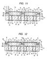
- Fig. 11 is a cross sectional view showing a step in a method of manufacturing the electronic part shown in Fig. 1;
- Fig. 12 is a cross sectional view showing a step in a method of manufacturing the electronic part shown in Fig. 1;
- Fig. 13 is a cross sectional view showing a step in a method of manufacturing the electronic part shown in Fig. 4;
- Fig. 14 is a cross sectional view showing a step in a method of manufacturing the electronic part shown in Fig. 4;
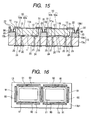
- Fig. 15 is a cross sectional view showing a step in a method of manufacturing the electronic part shown in Fig. 4;
- Fig. 16 is a plan view of an electronic part according to a seventh embodiment of the present invention;
- Fig. 17 is a cross sectional view of a conventional electronic part; and
- Fig. 18 is a cross sectional view of a conventional electronic part.
-
- Hereinafter, embodiments of the present invention will now be described with reference to the drawings.
- Fig. 1 is a cross sectional view of an electronic part according to a first embodiment of the present invention. The electronic part shown in Fig. 1 is formed by sealing a surface acoustic element in a concave portion provided in a case body made of ceramic.
- In the
case body 13 composed of a laminated substrate made of ceramic in the electronic part E1 shown in Fig. 1, a concave portion is formed by providing asidewall portion 13b on thebottom portion 13a. By this concave portion, anaccommodating portion 15 for accommodating anelectronic element 11 is formed. Thesubstrate 11c of theelectronic element 11 is accommodated in theaccommodating portion 15 so that thesurface 11d thereof is opposed to abottom surface 15a of theaccommodating portion 15, and thus thebottom surface 11b of thesubstrate 11c is directed upward. - The
electronic element 11 is formed withterminals terminals lands accommodating portion 15. Thelands portions bottom portion 13a through conductingportions bottom portion 13a of thecase body 13. - The
electronic element 11 is, for example, a band pass filter formed by using a surface acoustic element. The surface acoustic element has the structure that the teeth portions of a pair of teeth-shaped electrodes (IDT (inter-digital transducer) electrodes) which is made of conductive material having a low specific gravity are differently arranged on the surface of a piezoelectric substrate. The surface acoustic element having such a simple structure is the suitable element to miniature a filter, a resonator or a duplexer mounted in a mobile communication terminal. - The upper side of the
accommodating portion 15 is an open surface and, in order to close the open surface,seal material 16 made of resin is provided over a range from thebottom surface 11b of thesubstrate 11c of theelectronic element 11 to thesidewall portion 13b around theaccommodating portion 15 of thecase body 13. In addition, ametal film 17 is laminated on the seal material'16. Theseal material 16 is formed by thermosetting resin such as epoxy resin or polyimide resin. Particularly, it is preferable that epoxy resin having low water permeability is used. By sealing theaccommodating portion 15 with the sealingmaterial 16, theelectronic element 11 accommodated in theaccommodating portion 15 is sealed in theaccommodating portion 15. - In the electronic part shown in Fig. 1, the
bottom surface 11b of thesubstrate 11c of theelectronic element 11 is positioned on the same virtual plane A of an upper surface 13b1 of thesidewall portion 13b of thecase body 13. Accordingly, the gap is not formed between theseal material 16 and thebottom surface 11b of theelectronic element 11, thereby it becomes.easier to make the electronic part thin. Also, since theseal material 16 is made of resin, even when the positions of thebottom surface 11b of thesubstrate 11c and an upper surface 13b1 of thesidewall portion 13b are deviated, the deviation can be easily absorbed. - Furthermore, within the range that the
accommodating portion 15 is sealed with theseal material 16, thebottom surface 11b of thesubstrate 11c of theelectronic element 11 may be positioned at a height higher than an upper surface 13b1 of thesidewall portion 13b of thecase body 13. - In Fig. 1, the
seal material 16 has a uniform thickness throughout an overall area of thebottom surface 11b of thesubstrate 11c. There is a case that theseal material 16 is slightly drooped downward between thebottom surface 11b of thesubstrate 11c and the sidewall portion. - As shown in Fig. 1, a
conductive portion 22 and aconductive portion 23 composed of conductive material are provided at an outside and inside of thesidewall portion 13 of thecase body 13 of the electronic part E1. In addition, a connectingportion 25 is provided at a bottom surface of thecase body 13 and theconductive portion 24 passing through thebottom portion 13a of thecase body 13. Theconductive portions portion 25 are electrically connected, and the connectingportion 25 is grounded. By connecting theconductive portion 22 and themetal film 17, themetal film 17 is grounded, and thus the shield effect of themetal film 17 can be improved. - In addition, the
conductive portion 22 connected to themetal film 17 is formed inside agroove portion 30 provided at an outside of thesidewall portion 13b of thecase body 13. Alower end 30a of thegroove portion 30 is positioned inside thesidewall portion 13b of thecase body 13 so as not to be exposed to a bottom surface 13a1 of thecase body 13. Thereby, the solder can be prevented from being sucked into thegroove portion 30 when soldering the electronic part E1 on the wiring substrate. - The plan view of the state that the
metal film 17 of the electronic part of Fig. 1 is detached is shown in Fig. 2. Also, Fig. 1 is a cross sectional view when the electronic part cut along the line 1-1 in Fig. 2 is seen from the arrow direction. Fig. 3 is a cross sectional view of the electronic part E2 according to a second embodiment of the present invention. The electronic part E2 shown in Fig. 3 is different from the electronic part E1 shown in Fig. 1 only in that aconductive portion 40 and aconductive portion 41 composed of conductive material are provided inside thesidewall portion 13b of thecase body 13. Theconductive portions portion 25 are electrically connected and the connectingportion 25 is grounded. By connecting theconductive portion 40 and themetal film 17, themetal film 17 is grounded and thus the shield effect of themetal film 17 can be improved. - Figs. 4 and 5 are cross sectional views of electronic parts according to third and fourth embodiments of the present invention, respectively.
- In the electronic part E3 shown in Fig. 4, a
seal material 51 is formed over a range from a peripheral portion 11b1 of thebottom surface 11b of thesubstrate 11c of theelectronic element 11 to thecase body 13b, a through-hole 51a is formed in theseal material 51 on an inside portion 11b2 of thebottom surface 11b of thesubstrate 11c, thereby the area that themetal film 50 is directly laminated on thesubstrate 11c is provided. If themetal film 50 is directly laminated on thesubstrate 11c, the emitting effect of the Joule heat generated from theelectronic element 11 becomes increased. The surface of themetal film 50 is formed with irregularities composed of aconcave portion 50a and aconvex portion 50b on thebottom surface 11b of thesubstrate 11c, thereby increasing the surface area and thus further increasing the emitting effect of the Joule heat. - The electronic part E4 shown in Fig. 5 is similar to the electronic part E3 shown in Fig. 4 and is different from it in that, on an inside portion 11b2 of the
bottom surface 11b of thesubstrate 11c, a plurality of through-holes are formed in theseal material 52 and ametal film 53 is directly laminated on thesubstrate 11c in the through-hole. The surface of themetal film 53 is formed with irregularities composed of aconcave portion 53b and aconvex portion 53a on thebottom surface 11b of thesubstrate 11c. - The electronic part E4 shown in Fig. 5 has the same effect as the electronic part E3 shown in Fig. 4.
- The electronic parts E3, E4 shown in Figs. 4 and 5 does not need the expensive
conductive resin 6 between theelectronic element 1 and thecover body 4, unlike the conventional electronic part shown in Fig. 18, and thus the structure for efficiently emitting the Joule heat generated from theelectronic element 11 to an outside thereof can be realized with a low cost. - The electronic part E5 shown in Fig. 6 is similar to the electronic part E3 shown in Fig. 4 and is different from it in that the surface of
seal material 60 on thebottom surface 11b of thesubstrate 11c of theelectronic part 11 is formed with irregularities having aconcave portion 60b and aconvex portion 60a, without forming the through-hole in theseal material 60. Also, the surface of themetal film 61 laminated on theseal material 60 is formed with irregularities. - The electronic part E6 shown in Fig. 7 is similar to the electronic part E4 shown in Fig. 5 and is different from it in that the surface of
seal material 70 on thebottom surface 11b of thesubstrate 11c of theelectronic part 11 is formed with irregularities having aconcave portion 70b and aconvex portion 70a, without forming the through-hole in theseal material 70. Also, the surface of the metal film 71 laminated on theseal material 70 is formed with irregularities. - The electronic parts shown in Figs. 6 and 7 can realize the structure for efficiently emitting the Joule heat generated from the
electronic element 11 to an outside thereof with a low cost. - Now, a method of manufacturing the electronic part shown in Fig. 1 will be described.
- Figs. 8 to 12 are cross sectional views showing a method of manufacturing the electronic part shown in Fig. 1. First, the connecting
portion 21 and the connectingportion 25 are provided on the lower surfaces of thecase body 13 and theconductive portion 24 and theconductive portion 20 passing through thebottom portion 13a of thecase body 13, and theland 12 is formed on theconductive portion 24. Next, thesidewall portion 13b is formed by laminating the substrate on thebottom portion 13a of thecase body 13. Theconductive portion 22 and theconductive portion 23 composed of the conductive material are formed inside thesidewall portion 13b. Theconductive portion 22 is formed by laminating the substrate having ahole 80 therein on theconductive portion 23 and then plating the inner peripheral surface of thehole 80. - By providing the
sidewall portion 13b on thebottom portion 13a of thecase body 13, a concave portion is formed. By the concave portion, theaccommodating portion 15 for accommodating theelectronic element 11 is formed. - Next, the
electronic element 11 is accommodated in theaccommodating portion 15 so that thesurface 11d of thesubstrate 11c of theelectronic element 11 is opposed to abottom surface 15a of theaccommodating portion 15. Accordingly, thebottom surface 11b of thesubstrate 11c is directed upward. Theelectronic element 11 is formed with theterminals accommodating portion 15. - The
lands portions bottom portion 13a through theconductive portions bottom portion 13a of thecase body 13. - The
electronic element 11 is, for example, the band pass filter formed by using the surface acoustic element. Also, thebottom surface 11b of thesubstrate 11c of theelectronic element 11 is positioned on the same virtual plane A of an upper surface 13b1 of thesidewall portion 13b of thecase body 13. Alternatively, thesubstrate 11c may be arranged so that thebottom surface 11b of thesubstrate 11c is positioned at a height higher than an upper surface 13b1 of thesidewall portion 13b of thecase body 13. - The plan view of the electronic part at the step shown in Fig. 8 is shown in Fig. 9. In addition, although the case that two electronic parts are simultaneously formed is shown in Figs. 8 to 12, the number of the electronic parts which are simultaneously formed can be optionally determined.
- Next, as shown in Fig. 10, in order to close the open surface at the upper side of the accommodating.
portion 15, theresin seal material 16 is provided over a range from thebottom surface 11b of thesubstrate 11c of theelectronic element 11 to thesidewall portion 13b around theaccommodating portion 15 of thecase body 13 and is cured by applying heat. Theseal material 16 is formed by, for example, epoxy resin or polyimide resin. Particularly, it is preferable that epoxy resin having low water permeability is used. By sealing theaccommodating portion 15 with theseal material 16, theelectronic element 11 accommodated in theaccommodating portion 15 is sealed in theaccommodating portion 15. In Fig. 10, theseal material 16 has the uniform thickness throughout an overall area of thebottom surface 11b of thesubstrate 11c. Like the present embodiment, even when a plurality of the electronic parts are simultaneously formed, the overall electronic parts may be sealed with oneseal material 16. - Next, in the step shown in Fig. 11, the seal material on the
conductive portion 22 is removed by using a dicing blade D to expose an upper surface of theconductive portion 22 to an inside of thegroove portion 81. The dicing is performed with a lattice shape along a dotted line of the Fig. 9. Since the dicing step of Fig. 11 is to expose theconductive portion 22 extended in the thickness direction of thesidewall portion 13b of thecase body 13, it does not require high precision. If theconductive portion 23 is overlapped on the lower surface of theseal material 16 without forming theconductive portion 22 extended in the thickness direction of thesidewall portion 13b, the surface of theconductive portion 23 is exposed, thereby an expensive laser apparatus having high manufacturing precision is required. - Next, in the step shown in Fig. 12, the
metal film 17 is formed on theseal material 16 and the conductingportion 22 by a plating. Theconductive portions portion 25 are electrically connected and the connectingportion 25 is grounded. By connecting theconductive portion 22 and themetal film 17, themetal film 17 is grounded and thus the shield effect of themetal film 17 can be improved. - In addition, it is diced along a dashed dot line B-B and is separated into two electronic parts.
- When forming the electronic part shown in Fig. 4, after the step shown in Fig. 10, the through-
hole 51a is formed in theseal material 51 on an inside of thebottom surface 11b of thesubstrate 11c, as shown in Fig. 13, and an upper surface of theconductive portion 22 is exposed in the step shown in Fig. 14, and themetal film 50 is formed by a plating in the step shown in Fig. 15. At this time, theconcave portion 50a of themetal film 50 is directly laminated on thesubstrate 11c exposed in the through-hole 51a. Alternatively, theseal material 51 having the through-hole 51a therein may be arranged so that the through-hole 51a is positioned on an inside of thebottom surface 11b of thesubstrate 11c. - Also, instead of forming the through-hole in the seal material, by forming irregularities in the surface of the seal material, the electronic part shown in Fig. 6 or 7 can be formed.
- Also, in the above-mentioned embodiment, the
conductive portion 22 is formed by laminating the substrate having thehole 80 therein on theconductive portion 23 and by performing the plating on the inner peripheral surface of thehole 80. The shape of the hole is not limited to the circular shape, and theconductive portion 91 corresponding to theconductive portion 22 may be formed on the inner peripheral surface of therectangular hole 90 by a plating, as shown in Fig. 16.
Claims (17)
- An electronic part comprising:wherein the substrate is accommodated in the accommodating portion so that a surface of the substrate opposes a bottom surface of the accommodating portion and a bottom surface of the substrate is directed upward, a resin seal material is provided over a range from the bottom surface of the substrate to a sidewall portion around the accommodating portion of the case body, and a metal film is laminated on the seal material.a substrate on which an electronic element is mounted or is formed; anda case body having an accommodating part for accommodating the substrate,
- The electronic part according to claim 1,
wherein the bottom surface of the substrate is positioned on the same virtual plane of an upper surface of the sidewall portion of the case body. - The electronic part according to claim 1,
wherein the bottom surface of the substrate is positioned at a height higher than an upper surface of the sidewall portion of the case body. - The electronic part according to any of claims 1 to 3,
wherein the seal material has a uniform thickness throughout an overall area of the bottom surface of the substrate. - The electronic part according to any of claims 1 to 4,
wherein a surface of the seal material on the bottom surface of the substrate is formed with irregularities. - The electronic part according to any of claims 1 to 5,
wherein the seal material is formed over a range from a peripheral portion of the bottom surface of the substrate to the sidewall portion of the case body, a through-hole is formed in the seal material on an inside of the bottom surface of the substrate, thereby an area that the metal film is directly laminated on the substrate is provided. - The electric part according to claim 5 or 6,
wherein the surface of the metal film is formed with irregularities on the bottom surface of the substrate. - The electric part according to any of claims 1 to 7,
wherein the metal film is electrically connected to a connecting portion provided on a lower surface of the case body through a conductive portion provided at an outside or inside of a bottom portion of the case body and at an outside or inside of the sidewall portion of the case body. - The electronic part according to any of claims 1 to 8,
wherein a conductive portion is formed inside a groove portion provided at an outside of the sidewall portion of the case body, and a lower end of the groove portion is positioned inside the sidewall portion of the case body so that a bottom of the case body is not exposed. - A method of manufacturing an electronic part, comprising the steps of:(a) forming a concave portion in a case body to provide an accommodating portion;(b) accommodating a substrate on which an electronic element is mounted or formed in the accommodating portion so that a surface of the substrate opposes to a bottom surface of the accommodating portion and a bottom surface of the substrate is directed upward;(c) providing a resin seal material over a range from the bottom surface of the substrate to a sidewall portion around the accommodating portion of the case body; and(d) laminating a metal film on the seal material.
- The method according to claim 10,
wherein, in step (b), the substrate is arranged so that the bottom surface of the substrate is positioned at the same virtual plane of an upper surface of the sidewall portion of the case body. - The method according to claim 10,
wherein, in step (b), the substrate is arranged so that the bottom surface of the substrate is positioned at a height higher than an upper surface of the sidewall portion of the case body. - The method according to any of claims 10 to 12,
wherein, in step (c), the seal material has a uniform thickness throughout an overall area of the bottom surface of the substrate. - The method according to any of claims 10 to 13,
wherein, in step (c), a surface of the seal material on the bottom surface of the substrate is formed with irregularities. - The method according to any of claims 10 to 14,
wherein, in step (c), a through-hole is formed in the seal material on an inside of the bottom surface of the substrate, and, in step (d), the metal film is directly laminated on the substrate exposed to the through-hole. - The method according to claim 14 or 15,
wherein, in step (d), the metal film is formed so that the surface thereof has the irregularities on the bottom surface of the substrate. - The method according to any of claims 10 to 16, further comprising:wherein, in step (c), the seal material on the conductive portion is removed after covering the conductive portion by the seal material, and in step (d), the metal film and the conductive portion are connected to each other.before step (a), a step (e) of forming a connecting portion electrically connected to the electronic element and a connecting portion electrically connected to the metal film, on a bottom surface of the case body; andbefore step (a) or step (b), a step (f) of forming a conductive portion electrically connected to the connecting portion of a bottom surface of the case body at an outside or inside of the sidewall portion of the case body,
Applications Claiming Priority (2)
| Application Number | Priority Date | Filing Date | Title |
|---|---|---|---|
| JP2004027588 | 2004-02-04 | ||
| JP2004027588A JP2005223036A (en) | 2004-02-04 | 2004-02-04 | Electronic part and its manufacturing method |
Publications (1)
| Publication Number | Publication Date |
|---|---|
| EP1562289A2 true EP1562289A2 (en) | 2005-08-10 |
Family
ID=34675489
Family Applications (1)
| Application Number | Title | Priority Date | Filing Date |
|---|---|---|---|
| EP05002294A Withdrawn EP1562289A2 (en) | 2004-02-04 | 2005-02-03 | Electronic part and method of manufacturing the same |
Country Status (3)
| Country | Link |
|---|---|
| US (1) | US20050167137A1 (en) |
| EP (1) | EP1562289A2 (en) |
| JP (1) | JP2005223036A (en) |
Families Citing this family (4)
| Publication number | Priority date | Publication date | Assignee | Title |
|---|---|---|---|---|
| JP5094622B2 (en) * | 2008-08-04 | 2012-12-12 | 太陽誘電株式会社 | Circuit module and method for manufacturing circuit module |
| JP5275155B2 (en) * | 2009-06-26 | 2013-08-28 | セイコーインスツル株式会社 | Manufacturing method of electronic device |
| US9868632B2 (en) * | 2016-03-24 | 2018-01-16 | Infineon Technologies Ag | Molded cavity package with embedded conductive layer and enhanced sealing |
| JP6869698B2 (en) * | 2016-11-04 | 2021-05-12 | 太陽誘電株式会社 | Electronic device |
Family Cites Families (9)
| Publication number | Priority date | Publication date | Assignee | Title |
|---|---|---|---|---|
| JP2780649B2 (en) * | 1994-09-30 | 1998-07-30 | 日本電気株式会社 | Semiconductor device |
| US5572070A (en) * | 1995-02-06 | 1996-11-05 | Rjr Polymers, Inc. | Integrated circuit packages with heat dissipation for high current load |
| US5909058A (en) * | 1996-09-25 | 1999-06-01 | Kabushiki Kaisha Toshiba | Semiconductor package and semiconductor mounting part |
| US6404100B1 (en) * | 1999-10-18 | 2002-06-11 | Kabushiki Kaisha Toshiba | Surface acoustic wave apparatus and method of manufacturing the same |
| JP2001127088A (en) * | 1999-10-27 | 2001-05-11 | Mitsubishi Electric Corp | Semiconductor device |
| JP2001144218A (en) * | 1999-11-17 | 2001-05-25 | Sony Corp | Semiconductor device and method of manufacturing semiconductor device |
| CN1221076C (en) * | 2001-02-06 | 2005-09-28 | 松下电器产业株式会社 | Surface acoustic wave device, manufacturing method thereof, and electronic circuit device |
| TW536768B (en) * | 2001-08-03 | 2003-06-11 | Matsushita Electric Industrial Co Ltd | Method for fabricating semiconductor-mounting body and apparatus for fabricating semiconductor-mounting body |
| US6759266B1 (en) * | 2001-09-04 | 2004-07-06 | Amkor Technology, Inc. | Quick sealing glass-lidded package fabrication method |
-
2004
- 2004-02-04 JP JP2004027588A patent/JP2005223036A/en not_active Withdrawn
-
2005
- 2005-01-31 US US11/047,849 patent/US20050167137A1/en not_active Abandoned
- 2005-02-03 EP EP05002294A patent/EP1562289A2/en not_active Withdrawn
Also Published As
| Publication number | Publication date |
|---|---|
| US20050167137A1 (en) | 2005-08-04 |
| JP2005223036A (en) | 2005-08-18 |
Similar Documents
| Publication | Publication Date | Title |
|---|---|---|
| JP4712632B2 (en) | Elastic wave device and manufacturing method thereof | |
| CN100407467C (en) | Piezoelectric oscillator, portable telephone device using piezoelectric oscillator, and electronic equipment using piezoelectric oscillator | |
| US9751109B2 (en) | Acoustic wave device and method of fabricating the same | |
| CN1221076C (en) | Surface acoustic wave device, manufacturing method thereof, and electronic circuit device | |
| CN103378068A (en) | Circuit module and method of manufacturing the same | |
| JPWO2006001125A1 (en) | Piezoelectric device | |
| CN114208027B (en) | Piezoelectric vibration plate, piezoelectric vibration device, and method for manufacturing piezoelectric vibration device | |
| JP2013251323A (en) | Electronic component | |
| US9654081B2 (en) | Electronic component and manufacturing method therefor | |
| CN106233624A (en) | Crystal vibrating device and manufacturing method thereof | |
| JP4010293B2 (en) | Metal package manufacturing method | |
| JP5848079B2 (en) | Elastic wave device and manufacturing method thereof | |
| JP2007005948A (en) | Electronic component and manufacturing method thereof | |
| US20050167137A1 (en) | Electronic part and method of manufacturing the same | |
| CN114208032B (en) | Piezoelectric vibration device and manufacturing method thereof | |
| CN110034741B (en) | Elastic wave device | |
| US10784836B2 (en) | Piezoelectric vibration device and method for manufacturing the same | |
| JP4084188B2 (en) | Surface acoustic wave device | |
| JP2006120981A (en) | Electronic component and manufacturing method thereof | |
| JP2008135998A (en) | Elastic wave device and manufacturing method thereof | |
| JP2004173050A (en) | Quartz crystal resonator and manufacturing method thereof | |
| CN100474768C (en) | Surface acoustic wave device and method of manufacturing the same, IC card, and mobile electronic apparatus | |
| JP2000236230A (en) | Surface acoustic wave filter | |
| JP2005217670A (en) | Surface acoustic wave device and communication device | |
| JP2013197921A (en) | Manufacturing method of electronic component and electronic component |
Legal Events
| Date | Code | Title | Description |
|---|---|---|---|
| PUAI | Public reference made under article 153(3) epc to a published international application that has entered the european phase |
Free format text: ORIGINAL CODE: 0009012 |
|
| AK | Designated contracting states |
Kind code of ref document: A2 Designated state(s): AT BE BG CH CY CZ DE DK EE ES FI FR GB GR HU IE IS IT LI LT LU MC NL PL PT RO SE SI SK TR |
|
| AX | Request for extension of the european patent |
Extension state: AL BA HR LV MK YU |
|
| STAA | Information on the status of an ep patent application or granted ep patent |
Free format text: STATUS: THE APPLICATION IS DEEMED TO BE WITHDRAWN |
|
| 18D | Application deemed to be withdrawn |
Effective date: 20070301 |