EP1562236A2 - Transparent electrode layer, semiconductor light emitting device including the same, and method of forming the transparent electrode layer - Google Patents
Transparent electrode layer, semiconductor light emitting device including the same, and method of forming the transparent electrode layer Download PDFInfo
- Publication number
- EP1562236A2 EP1562236A2 EP04256921A EP04256921A EP1562236A2 EP 1562236 A2 EP1562236 A2 EP 1562236A2 EP 04256921 A EP04256921 A EP 04256921A EP 04256921 A EP04256921 A EP 04256921A EP 1562236 A2 EP1562236 A2 EP 1562236A2
- Authority
- EP
- European Patent Office
- Prior art keywords
- electrode layer
- layer
- electrode
- additive element
- type
- Prior art date
- Legal status (The legal status is an assumption and is not a legal conclusion. Google has not performed a legal analysis and makes no representation as to the accuracy of the status listed.)
- Withdrawn
Links
Images




Classifications
-
- H—ELECTRICITY
- H10—SEMICONDUCTOR DEVICES; ELECTRIC SOLID-STATE DEVICES NOT OTHERWISE PROVIDED FOR
- H10H—INORGANIC LIGHT-EMITTING SEMICONDUCTOR DEVICES HAVING POTENTIAL BARRIERS
- H10H20/00—Individual inorganic light-emitting semiconductor devices having potential barriers, e.g. light-emitting diodes [LED]
- H10H20/80—Constructional details
- H10H20/83—Electrodes
- H10H20/832—Electrodes characterised by their material
- H10H20/833—Transparent materials
-
- H—ELECTRICITY
- H01—ELECTRIC ELEMENTS
- H01S—DEVICES USING THE PROCESS OF LIGHT AMPLIFICATION BY STIMULATED EMISSION OF RADIATION [LASER] TO AMPLIFY OR GENERATE LIGHT; DEVICES USING STIMULATED EMISSION OF ELECTROMAGNETIC RADIATION IN WAVE RANGES OTHER THAN OPTICAL
- H01S5/00—Semiconductor lasers
- H01S5/04—Processes or apparatus for excitation, e.g. pumping, e.g. by electron beams
- H01S5/042—Electrical excitation ; Circuits therefor
- H01S5/0425—Electrodes, e.g. characterised by the structure
- H01S5/04252—Electrodes, e.g. characterised by the structure characterised by the material
- H01S5/04253—Electrodes, e.g. characterised by the structure characterised by the material having specific optical properties, e.g. transparent electrodes
-
- H—ELECTRICITY
- H10—SEMICONDUCTOR DEVICES; ELECTRIC SOLID-STATE DEVICES NOT OTHERWISE PROVIDED FOR
- H10D—INORGANIC ELECTRIC SEMICONDUCTOR DEVICES
- H10D62/00—Semiconductor bodies, or regions thereof, of devices having potential barriers
- H10D62/80—Semiconductor bodies, or regions thereof, of devices having potential barriers characterised by the materials
- H10D62/85—Semiconductor bodies, or regions thereof, of devices having potential barriers characterised by the materials being Group III-V materials, e.g. GaAs
-
- H—ELECTRICITY
- H10—SEMICONDUCTOR DEVICES; ELECTRIC SOLID-STATE DEVICES NOT OTHERWISE PROVIDED FOR
- H10D—INORGANIC ELECTRIC SEMICONDUCTOR DEVICES
- H10D64/00—Electrodes of devices having potential barriers
- H10D64/01—Manufacture or treatment
- H10D64/011—Manufacture or treatment of electrodes ohmically coupled to a semiconductor
- H10D64/0116—Manufacture or treatment of electrodes ohmically coupled to a semiconductor to Group III-V semiconductors
-
- H—ELECTRICITY
- H10—SEMICONDUCTOR DEVICES; ELECTRIC SOLID-STATE DEVICES NOT OTHERWISE PROVIDED FOR
- H10D—INORGANIC ELECTRIC SEMICONDUCTOR DEVICES
- H10D64/00—Electrodes of devices having potential barriers
- H10D64/60—Electrodes characterised by their materials
- H10D64/62—Electrodes ohmically coupled to a semiconductor
-
- H—ELECTRICITY
- H01—ELECTRIC ELEMENTS
- H01S—DEVICES USING THE PROCESS OF LIGHT AMPLIFICATION BY STIMULATED EMISSION OF RADIATION [LASER] TO AMPLIFY OR GENERATE LIGHT; DEVICES USING STIMULATED EMISSION OF ELECTROMAGNETIC RADIATION IN WAVE RANGES OTHER THAN OPTICAL
- H01S5/00—Semiconductor lasers
- H01S5/04—Processes or apparatus for excitation, e.g. pumping, e.g. by electron beams
- H01S5/042—Electrical excitation ; Circuits therefor
- H01S5/0421—Electrical excitation ; Circuits therefor characterised by the semiconducting contacting layers
-
- H—ELECTRICITY
- H01—ELECTRIC ELEMENTS
- H01S—DEVICES USING THE PROCESS OF LIGHT AMPLIFICATION BY STIMULATED EMISSION OF RADIATION [LASER] TO AMPLIFY OR GENERATE LIGHT; DEVICES USING STIMULATED EMISSION OF ELECTROMAGNETIC RADIATION IN WAVE RANGES OTHER THAN OPTICAL
- H01S5/00—Semiconductor lasers
- H01S5/04—Processes or apparatus for excitation, e.g. pumping, e.g. by electron beams
- H01S5/042—Electrical excitation ; Circuits therefor
- H01S5/0425—Electrodes, e.g. characterised by the structure
- H01S5/04256—Electrodes, e.g. characterised by the structure characterised by the configuration
- H01S5/04257—Electrodes, e.g. characterised by the structure characterised by the configuration having positive and negative electrodes on the same side of the substrate
-
- H—ELECTRICITY
- H01—ELECTRIC ELEMENTS
- H01S—DEVICES USING THE PROCESS OF LIGHT AMPLIFICATION BY STIMULATED EMISSION OF RADIATION [LASER] TO AMPLIFY OR GENERATE LIGHT; DEVICES USING STIMULATED EMISSION OF ELECTROMAGNETIC RADIATION IN WAVE RANGES OTHER THAN OPTICAL
- H01S5/00—Semiconductor lasers
- H01S5/30—Structure or shape of the active region; Materials used for the active region
- H01S5/32—Structure or shape of the active region; Materials used for the active region comprising PN junctions, e.g. hetero- or double- heterostructures
- H01S5/323—Structure or shape of the active region; Materials used for the active region comprising PN junctions, e.g. hetero- or double- heterostructures in AIIIBV compounds, e.g. AlGaAs-laser, InP-based laser
- H01S5/32308—Structure or shape of the active region; Materials used for the active region comprising PN junctions, e.g. hetero- or double- heterostructures in AIIIBV compounds, e.g. AlGaAs-laser, InP-based laser emitting light at a wavelength less than 900 nm
- H01S5/32341—Structure or shape of the active region; Materials used for the active region comprising PN junctions, e.g. hetero- or double- heterostructures in AIIIBV compounds, e.g. AlGaAs-laser, InP-based laser emitting light at a wavelength less than 900 nm blue laser based on GaN or GaP
-
- H—ELECTRICITY
- H10—SEMICONDUCTOR DEVICES; ELECTRIC SOLID-STATE DEVICES NOT OTHERWISE PROVIDED FOR
- H10D—INORGANIC ELECTRIC SEMICONDUCTOR DEVICES
- H10D62/00—Semiconductor bodies, or regions thereof, of devices having potential barriers
- H10D62/80—Semiconductor bodies, or regions thereof, of devices having potential barriers characterised by the materials
- H10D62/85—Semiconductor bodies, or regions thereof, of devices having potential barriers characterised by the materials being Group III-V materials, e.g. GaAs
- H10D62/8503—Nitride Group III-V materials, e.g. AlN or GaN
-
- H—ELECTRICITY
- H10—SEMICONDUCTOR DEVICES; ELECTRIC SOLID-STATE DEVICES NOT OTHERWISE PROVIDED FOR
- H10H—INORGANIC LIGHT-EMITTING SEMICONDUCTOR DEVICES HAVING POTENTIAL BARRIERS
- H10H20/00—Individual inorganic light-emitting semiconductor devices having potential barriers, e.g. light-emitting diodes [LED]
- H10H20/80—Constructional details
- H10H20/81—Bodies
- H10H20/822—Materials of the light-emitting regions
- H10H20/824—Materials of the light-emitting regions comprising only Group III-V materials, e.g. GaP
- H10H20/825—Materials of the light-emitting regions comprising only Group III-V materials, e.g. GaP containing nitrogen, e.g. GaN
Definitions
- the present invention relates to a predetermined material layer, a method of forming the same, and a light emitting device including the same, and more particularly, to an electrode layer, a method of forming the electrode layer, and a light emitting device including the electrode layer.
- a light emitting device such as a light emitting diode (LED) or a laser diode (LD)
- LED light emitting diode
- LD laser diode
- a light emitting device in which a material layer is disposed in an improved manner between an electrode layer and an active layer is widely used.
- a width of a current inflow path ranging from the electrode layer to the active layer is limited such that light is emitted in a limited region.
- the electrode layer is a material layer through which a current for light emission firstly passes and in ohmic contact with a compound semiconductor layer, for example, a p-type GaN compound semiconductor layer, it is essential to reduce the resistance of the electrode layer to lower the drive voltage of the light emitting device.
- FIG. 1 is a cross-sectional view of a light emitting device including a conventional electrode layer.
- the light emitting device includes an n-GaN layer 6, an active layer 8, and a p-GaN layer 10, which are sequentially stacked, and a p-type electrode is formed on the p-GaN layer 10.
- the p-type electrode includes a first electrode layer 12 and a second electrode layer 14, which are sequentially formed.
- the first electrode layer 12 is formed of Ni
- the second electrode layer 14 is formed of Au.
- the p-type electrode since the p-type electrode is formed in a thermodynamic relationship with the first and second electrode layers 12 and 14, the p-type electrode may be formed of only several predetermined materials.
- the p-type electrode when the p-type electrode is formed of a Ni layer and an Au layer, the p-type electrode may have a high resistance and a low transmissivity. Thus, use of this p-type electrode may be limited.
- an electrode structure or layer including a first electrode layer and a second electrode layer, which are sequentially stacked.
- the first electrode layer is formed of indium oxide added by an additive element.
- the additive element may include at least one selected from the group consisting of Mg, Ag, Zn, Sc, Hf, Zr, Te, Se, Ta, W, Nb, Cu, Si, Ni, Co, Mo, Cr, Mn, Hg, Pr, and La.
- An addition ratio of the additive element to the indium oxide may be in the range of 0.001 to 49 atomic percent.
- the thickness of the first electrode layer may be in the range of 0.1 to 500 nm.
- the second electrode layer may be a metal layer or a transparent conductive oxide (TCO) layer.
- the metal layer may be formed of Au, Pd, Pt, or Ru.
- the TCO layer may be formed of indium tin oxide (ITO), zinc-doped indium tin oxide (ZITO), zinc indium oxide (ZIO), gallium indium oxide (GIO), zinc tin oxide (ZTO), fluorine-doped tin oxide (FTO), aluminum-doped zinc oxide (AZO), gallium-doped zinc oxide (GZO), In 4 Sn 3 O 12 , or zinc magnesium oxide (Zn 1-x Mg x O, 0 ⁇ x ⁇ 1).
- the thickness of the second electrode layer may be in the range of 0.1 to 500 nm.
- a light emitting device comprising at least an n-type compound semiconductor layer, an active layer, and a p-type compound semiconductor layer, which are disposed between an n-type electrode layer and a p-type electrode layer.
- the p-type electrode layer includes a first electrode layer and a second electrode layer, which are sequentially stacked, and the first electrode layer is formed of indium oxide added by an additive element.
- a method of forming an electrode layer comprises forming a first electrode layer on a substrate; forming a second electrode layer on the first electrode layer; and annealing the resultant structure where the second electrode layer is formed.
- the first electrode layer is formed of indium oxide added by an additive element.
- the resultant structure may be annealed in an atmosphere including at least one selected from the group consisting of N, Ar, He, O, H, and air at a temperature of about 200 to 700 °C for 10 seconds to 2 hours.
- the first electrode layer and the second electrode layer may be formd using an e-beam & thermal evaporator.
- An electrode structure according to the present invention has a low resistance and a high transmissivity.
- the light emitting device can require only a low drive voltage and have a high transmissivity, thereby greatly improving a luminous efficiency.
- the present invention provides an electrode structure having a relatively low resistance and a high transmissivity.
- the present invention also provides a light emitting device including the electrode layer.
- the present invention further provides a method of forming the electrode layer.
- FIG. 2 is a cross-sectional view of an electrode structure according to the present invention.
- the p-type electrode 22 is disposed on a p-type compound semiconductor layer 20.
- the p-type electrode 22 includes a first electrode layer 22a and a second electrode layer 22b, which are sequentially stacked.
- the first electrode layer 22a is formed of indium oxide, such as In 2 O 3 , which is added by an additive element.
- the additive element may improve an ohmic characteristic of the first electrode layer 22a by adjusting characteristics of indium oxide, such as band gap, electron affinity, and work function.
- the additive element can be a metal material, which increases an effective carrier concentration of the p-type compound semiconductor layer 20 and readily reacts with elements constituting the p-type compound semiconductor layer 20 except nitrogen.
- the additive element may be an element that reacts to Ga prior to N.
- Ga of the p-type compound semiconductor layer 20 reacts to the first electrode layer 22a, thus generating Ga vacancies in the surface of the p-type compound semiconductor layer 20.
- the Ga vacancies function as a p-type dopant, an effective concentration of p-type carriers in the surface of p-type compound semiconductor layer 20 increases.
- the first electrode layer 22a may be formed of a material, which reacts to a Ga 2 O 3 layer, which is a native oxide layer that remains on the p-type compound semiconductor layer 20 during formation of the first electrode layer 22a, to generate transparent conductive oxide.
- the Ga 2 O 3 layer serves as a barrier to flow of carriers at an interface between the p-type compound semiconductor layer 20 and the first electrode layer 22a. In this case, a tunneling conduction phenomenon may occur at the interface between the first electrode layer 22a and the p-type compound semiconductor layer 20, thus improving the ohmic characteristic of the first electrode layer 22a.
- the additive element for the first electrode layer 22a may be at least one of Mg, Ag, Zn, Sc, Hf, Zr, Te, Se, Ta, W, Nb, Cu, Si, Ni, Co, Mo, Cr, Mn, Hg, Pr, and La.
- an addition ratio of the additive element to indium oxide is in the range of 0.001 to 49 atomic percent.
- the second electrode layer 22b is a metal layer or a transparent conductive oxide (TCO) layer.
- the metal layer may be formed of Au, Pd, Pt, or Ru.
- the TCO layer may be formed of indium tin oxide (ITO), zinc-doped indium tin oxide (ZITO), zinc indium oxide (ZIO), gallium indium oxide (GIO), zinc tin oxide (ZTO), fluorine-doped tin oxide (FTO), aluminum-doped zinc oxide (AZO), gallium-doped zinc oxide (GZO), In 4 Sn 3 O 12 , or zinc magnesium oxide (Zn 1-x Mg x O, 0 ⁇ x ⁇ 1).
- the oxide layer may be, for example, a Zn 2 ln 2 O 5 layer, a GalnO 3 layer, a ZnSnO 3 layer, an F-doped SnO 2 layer, an Al-doped ZnO layer, a Ga-doped ZnO layer, a MgO layer, or a ZnO layer.
- the thickness of the second electrode layer 22b is in the range of 0.1 to 500 nm.
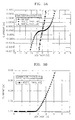
- FIG. 3A is a graph showing a measurement result of a current-voltage (C-V) characteristic of an electrode layer (MIO/Au) according to a first embodiment of the present invention.
- the electrode layer includes a first electrode layer 22a formed of magnesium-doped indium oxide (MIO) and a second electrode layer 22b formed of Au disposed on the first electrode layer 22a.
- the first electrode layer 22a and the second electrode layer 22b were formed to a thickness of about 100 nm and 5 nm, respectively.
- the inventors formed a first electrode layer 22a on a p-type GaN layer to a thickness of 100 nm and then formed a second electrode layer 22b on the first electrode layer 22a to a thickness of 5 nm.
- the first electrode layer 22a was formed using MIO obtained by adding Mg, which is one of the enumerated additive elements, to indium oxide on the p-type GaN layer 20, which includes GaN having a carrier concentration of 4 - 5 ⁇ 10 17 cm -3 as a main element.
- the second electrode layer 22b was deposited using Au on the first electrode layer 22a.
- the inventors measured the electrical characteristic of the resultant structure where the first and second electrode layers 22a and 22b are formed.
- the electrical characteristic of the electrode layer (MIO/Au) was measured before an annealing process (i.e., as deposited) and after the electrode layer was annealed at 430°C and 530°C, respectively, in an air atmosphere for 1 minute each time.
- V-C voltage-current
- nonlinear C-V characteristic i.e., a rectifying characteristic
- a linear C-V characteristic including information on ohmic contact was exhibited. Also, it can be seen that noncontact resistance was in a low range of 10 -3 to 10 -5 ⁇ cm 2 .
- indium oxide that is doped with or mixed with a predetermined element in order to control a band gap, an electron affinity, and a work function, which determine the electrical characteristic of the first electrode layer 22a being in contact with the p-type compound semiconductor layer 20, should have excellent optical transmissivity and conductivity.
- the first electrode layer 22a which is formed of this indium oxide, reacts with Ga 2 O 3 , which is an oxide layer disposed on the p-type compound semiconductor layer 20, during the annealing process, thus generating a TCO layer, i.e., a GalnO 3 layer.
- Ga vacancies are formed in the surface of the p-type compound semiconductor layer 20, thereby increasing an effective concentration of holes around the surface of the p-type compound semiconductor layer 20.
- the GalnO 3 layer has a large work function, when contacting the p-type compound semiconductor layer 20, the GalnO 3 layer can reduce the height and width of a Schottky barrier, thereby improving an ohmic contact characteristic and optical transmissivity.
- FIG. 3B is a graph showing a measurement result of a drive voltage of an InGaN blue light emitting diode (LED) including the electrode layer of FIG. 3A.
- LED InGaN blue light emitting diode
- the electrode layer (MIO/Au) was annealed at a temperature of 430 °C in an air atmosphere for 1 minute.
- the blue LED including the electrode layer (MIO/Au) as a p-type electrode layer has an improved drive voltage characteristic.
- FIG. 4A is a graph showing a measurement result of a C-V characteristic of an electrode layer (CIO/ZITO) according to a second embodiment of the present invention.
- the electrode layer (CIO/ZITO) includes a first electrode layer formed of copper-doped indium oxide (CIO) and a second electrode layer formed of ZITO disposed on the first electrode layer.
- the first electrode layer and the second electrode layer were formed to a thickness of 10 nm and 200 nm, respectively.
- the electrode layer (CIO/ZITO) was annealed at a temperature of about 530 °C in an air atmosphere for 1 minute.
- the electrode layer (CIO/ZITO) had a nonlinear C-V characteristic and a low noncontact resistance of 10 -3 to 10 -5 ⁇ cm 2 .
- a distance between adjacent electrodes was 4 ⁇ m.
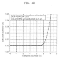
- FIG. 4B is a graph showing a measurement result of a drive voltage of an InGaN blue LED including the electrode layer of FIG. 4A.
- the blue LED including the electrode layer (CIO/ZITO) as a p-type electrode layer has an improved drive voltage characteristic.
- FIG. 5A is a graph showing a measurement result of a C-V characteristic of an electrode layer (CIO/ITO) according to a third embodiment of the present invention.
- the electrode layer (CIO/ITO) includes a first electrode layer formed of CIO and a second electrode layer formed of ITO disposed on the first electrode layer.
- the first electrode layer and the second electrode layer were formed to a thickness of about 10 nm and 200 nm, respectively.
- the electrode layer (CIO/ITO) was annealed at a temperature of about 530 °C in an air atmosphere for 1 minute.
- the electrode layer (CIO/ITO) had a nonlinear C-V characteristic and a low noncontact resistance of 10 -3 to 10 -5 ⁇ cm 2 .
- a distance between adjacent electrodes was 4 ⁇ m.
- FIG. 5B is a graph showing a measurement result of a drive voltage of an InGaN blue LED including an electrode layer (CIO/ITO) formed according to the third embodiment of the present invention.
- a first electrode layer and a second electrode layer were formed to a thickness of about 2.5 nm and 400 nm, respectively.
- a drive voltage of the blue LED including the electrode layer (CIO/ITO) was measured when the electrode layer was annealed at a temperature of 630 °C and 700 °C, respectively, in an air atmosphere for 1 minute each time, and compared with a drive voltage of an InGaN blue LED including a conventional electrode layer (Ni/Au).
- the blue LED including the electrode layer (CIO/ITO) as a p-type electrode layer has an improved drive voltage characteristic.
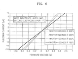
- FIG. 6 is a graph showing a measurement result of a C-V characteristic of an electrode layer (MIO/ITO) according to a fourth embodiment of the present invention.
- the electrode layer (MIO/ITO) includes a first electrode layer formed of MIO and a second electrode layer formed of ITO disposed on the first electrode layer.
- the first electrode layer and the second electrode layer were formed to a thickness of about 10 nm and 400 nm, respectively.
- the electrical characteristics of the electrode layer (MIO/ITO) were measured when it was annealed at a temperature of 500 °C, 550 °C, 600 °C, and 700 °C, respectively, in an air atmosphere for 1 minute each time.
- the electrode layer (MIO/ITO) had a linear C-V characteristic and a low noncontact resistance of 10 -3 to 10 -5 ⁇ cm 2 .
- a distance between adjacent electrodes was 4 ⁇ m.
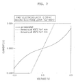
- FIG. 7 is a graph showing a measurement result of a C-V characteristic of an electrode layer (CIO/Au) formed according to a fifth embodiment of the present invention.
- the electrode layer (CIO/Au) includes a first electrode layer formed of CIO and a second electrode layer formed of Au disposed on the first electrode layer.
- the first electrode layer and the second electrode layer were formed to a thickness of about 5 nm and 100 nm, respectively.
- the electrical characteristics of the electrode layer (CIO/Au) were measured before an annealing process (i.e., as deposited) and after the electrode layer was annealed at 400°C and 450°C, respectively, in an air atmosphere for 1 minute each time.
- the electrode layer (CIO/Au) had a linear C-V characteristic and a low noncontact resistance of 10 -3 to 10 -5 ⁇ cm 2 .
- a distance between adjacent electrodes was 4 ⁇ m.
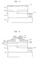
- FIGS. 8 and 9 are cross-sectional views illustrating light emitting devices including the electrode layers according to the present invention.
- FIG. 8 is a cross-sectional view of an LED including the electrode layer of FIG. 2 as a p-type electrode
- FIG. 9 is a cross-sectional view of an LD including the electrode layer of FIG. 2 as a p-type electrode.
- the LED includes an n-GaN layer 102 disposed on a substrate 100.
- the n-GaN layer 102 is divided into a first region R1 and a second region R2. There is a step difference between the first region R1 and the second region R2.
- the second region R2 is formed to a smaller thickness than the first region R1.
- An active layer 104, a p-GaN layer 106, and a p-type electrode 108 are sequentially formed on the first region R1 of the n-GaN layer 102.
- An n-type electrode 120 is formed on the second region R2 of the n-GaN layer 102.
- the LD includes an n-GaN layer 102 disposed on a substrate 100.
- the n-GaN layer 102 is divided into a first region R1 and a second region R2 like the LED shown in FIG. 5, and an n-type electrode 220 is formed on the second region R2.
- an n-clad layer 204, an n-type waveguide layer 206 having a higher refractive index than the n-clad layer 204, an active layer 208 having a higher refractive index than the n-type waveguide layer 206, and a p-type waveguide layer 210 having a lower refractive index than the active layer 208 are sequentially formed.
- a central upper portion of the p-clad layer 212 protrudes upward to form a ridge.
- a p-GaN layer 214 is formed as a contact layer on the protruding portion of the p-clad layer 212.
- An exposed surface of the p-clad layer 212 is covered by a protective layer 216, which also covers both outer portions of the p-GaN layer 214.
- a p-type electrode 218 is formed on the protective layer 216 to contact the exposed surface of the p-GaN layer 214.
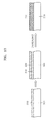
- FIG. 10 illustrates a method of forming an electrode layer according to the present invention.
- a first electrode layer 310 is formed on a p-type compound semiconductor layer 300, for example, a p-type GaN layer.
- the first electrode layer 310 is formed by adding an additive element to indium oxide, for example, In 2 O 3 .
- the additive element may be at least one of Mg, Ag, Zn, Sc, Hf, Zr, Te, Se, Ta, W, Nb, Cu, Si, Ni, Co, Mo, Cr, Mn, Hg, Pr, and La.
- An addition ratio of the additive element to the indium oxide ranges from 0.001 to 49 atomic percent.
- the first electrode layer 310 may be formed to a thickness of 0.1 to 500 nm.
- a second electrode layer 320 is formed on the first electrode layer 310 to a thickness of 0.1 to 500 nm.
- the second electrode layer 320 is a metal layer or a TCO layer.
- the metal layer may be formed of Au, Pd, Pt, or Ru.
- the TCO layer may be formed of ITO, ZITO, ZIO, GIO, ZTO, FTO, AZO, GZO, In 4 Sn 3 O 12 , or Zn 1-x Mg x O (0 ⁇ x ⁇ 1).
- the oxide layer may be, for example, a Zn 2 In 2 O 5 layer, a GaInO 3 layer, a ZnSnO 3 layer, an F-doped SnO 2 layer, an Al-doped ZnO layer, a Ga-doped ZnO layer, a MgO layer, or a ZnO layer.
- the first and second electrode layers 310 and 320 can be formed using an electronic beam (e-beam) & thermal evaporator or a dual-type thermal evaporator. Also, the first and second electrode layers 310 and 320 can be formed by physical vapor deposition (PVD), chemical vapor deposition (CVD), or plasma laser deposition (PLD).
- PVD physical vapor deposition
- CVD chemical vapor deposition
- PLD plasma laser deposition
- the first and second electrode layers 310 and 320 can be deposited at a temperature of about 20 to 1500°C under a reactor pressure of an atmospheric pressure to 10 -12 Torr.
- the resultant structure is annealed in an atmosphere of a gas including at least one of N, Ar, He, O, H, and air.
- the annealing process is performed at a temperature of about 200 to 700°C for 10 seconds to 2 hours.
- elements constituting the first and second electrode layers 310 and 320 may be mixed with one another so that a single electrode layer 330 may be formed on the p-type compound semiconductor substrate 300.
- the first and second electrode layers 310 and 320 may be separately formed on the p-type compound semiconductor substrate 300.
- the surface of a structure, in which a p-type GaN-based compound semiconductor layer 300 is formed on a substrate was washed in an ultrasonic bath at a temperature of 60°C using trichloroethylene (TCE), acetone, methanol, and distilled water, respectively, for 5 minutes each time. Then, the resultant structure was hard baked at a temperature of 100°C for 10 minutes to remove the remaining moisture from this sample.
- TCE trichloroethylene
- a photoresist layer was spin-coated on the p-type compound semiconductor layer 300 at 4,500 RPM.
- the resultant structure was soft baked at a temperature of 85°C for 15 minutes.
- the sample was aligned with a mask, exposed to ultraviolet rays (UV) of 22.8 mW for 15 seconds, and dipped in a solution containing a mixture of a developing solution with distilled water in a ratio of 1: 4 for 25 seconds.
- UV ultraviolet rays
- a first electrode layer 310 was formed on the resultant structure using an e-beam evaporator.
- BOE buffered oxide etchant
- the first electrode layer 310 was deposited by mounting an object of reaction, which is formed by sintering a mixture of indium oxide with MgO in a ratio of 9: 1, on a mounting stage.
- a second electrode layer 320 was deposited using Au, a lift-off process was carried out using acetone, and the sample was loaded into a rapid thermal annealing (RTA) furnace and annealed at a temperature of about 430 to 530°C for 1 minute. As a result, an electrode layer 330 was formed.
- RTA rapid thermal annealing
- the foregoing method of forming the electrode layer can be applied to manufacture the light emitting devices shown in FIGS. 8 and 9.
- the electrode layer of the present invention has a lower resistance and higher transmissivity than conventional electrode layers.
- a first electrode layer of the present invention can be formed to a greater thickness of about 0.1 to 500 nm. Thus, even if the first electrode layer is 100 nm thick, the electrode layer of the present invention can exhibit a low contact resistance and high transmissivity.
- the electrode layer of the present invention when used for a light emitting device, the light emitting device can require only a low drive voltage and have a high transmissivity, thereby greatly improving a luminous efficiency.
- an electrode layer of the present invention can applied to not only the light emitting devices shown in FIGS. 8 and 9 but also other light emitting devices and other devices requiring an electrode with a low resistance.
Landscapes
- Physics & Mathematics (AREA)
- Condensed Matter Physics & Semiconductors (AREA)
- General Physics & Mathematics (AREA)
- Electromagnetism (AREA)
- Optics & Photonics (AREA)
- Led Devices (AREA)
- Electroluminescent Light Sources (AREA)
- Electrodes Of Semiconductors (AREA)
Abstract
Description
Claims (20)
- An electrode structure including a first electrode layer and a second electrode layer, which are sequentially stacked,
wherein the first electrode layer is formed of indium oxide together with an additive element. - The electrode structure of claim 1, wherein the additive element includes at least one selected from the group consisting of Mg, Ag, Zn, Sc, Hf, Zr, Te, Se, Ta, W, Nb, Cu, Si, Ni, Co, Mo, Cr, Mn, Hg, Pr, and La.
- The electrode structure of claim 2, wherein an addition ratio of the additive element to the indium oxide is in the range of 0.001 to 49 atomic percent.
- The electrode structure of any preceding claim, wherein the thickness of the first electrode layer is in the range of 0.1 to 500 nm.
- The electrode structure of any preceding claim, wherein the second electrode layer is a metal layer.
- The electrode structure of claim 5, wherein the metal layer is formed of one selected from the group consisting of Au, Pd, Pt, and Ru.
- The electrode structure of any of claims 1 to 4, wherein the second electrode layer is a transparent conductive oxide layer.
- The electrode structure of claim 7, wherein the oxide layer is formed of one selected from the group consisting of ITO, ZITO, ZIO, GIO, ZTO, FTO, AZO, GZO, In4Sn3O12, and Zn1-xMgxO (0 ≤ x ≤ 1).
- A light emitting device comprising at least an n-type compound semiconductor layer, an active layer, and a p-type compound semiconductor layer, which are disposed between an n-type electrode structure and a p-type electrode structure,
wherein the p-type electrode includes an electrode structure according to any preceding claim,
and the first electrode layer is formed of indium oxide added by an additive element. - A method of forming an electrode structure, the method comprising:wherein the first electrode layer is formed of indium oxide added by an additive element.forming a first electrode layer on a substrate;forming a second electrode layer on the first electrode layer; andannealing the resultant structure where the second electrode layer is formed,
- The method of 10, wherein the additive element includes at least one selected from the group consisting of Mg, Ag, Zn, Sc, Hf, Zr, Te, Se, Ta, W, Nb, Cu, Si, Ni, Co, Mo, Cr, Mn, Hg, Pr, and La.
- The method of claim 11, wherein an addition ratio of the additive element to the indium oxide is in the range of 0.001 to 49 atomic percent.
- The method of claim 10, 11 or 12, wherein the first electrode layer is formed to a thickness of 0.1 to 500 nm.
- The method of any of claims 10 to 13, wherein the second electrode layer is formed of a metal.
- The method of claim 14, wherein the metal layer is formed of one selected from the group consisting of Au, Pd, Pt, and Ru.
- The method of any of claims 10 to 13, wherein the second electrode layer is formed of a transparent conductive oxide.
- The method of claim 16, wherein the oxide layer is formed of one selected from the group consisting of ITO, ZITO, ZIO, GIO, ZTO, FTO, AZO, GZO, In4Sn3O12, and Zn1-xMgxO (0 ≤ x ≤ 1).
- The method of any of claims 10 to 17, wherein the annealing of the resultant structure is performed in an atmosphere including at least one selected from the group consisting of N, Ar, He, O, H, and air.
- The method of any of claims 10 to 18, wherein the annealing of the resultant structure is performed at a temperature of about 200 to 700 °C for 10 seconds to 2 hours.
- The method of any of claims 10 to 19, wherein the forming of the first electrode layer and the forming of the second electrode layer are performed using an e-beam & thermal evaporator.
Applications Claiming Priority (4)
| Application Number | Priority Date | Filing Date | Title |
|---|---|---|---|
| KR20040007233 | 2004-02-04 | ||
| KR2004007233 | 2004-02-04 | ||
| KR1020040068295A KR100764458B1 (en) | 2004-02-04 | 2004-08-28 | Electrode layer, light generating device comprising the same and method of forming the same |
| KR2004068295 | 2004-08-28 |
Publications (2)
| Publication Number | Publication Date |
|---|---|
| EP1562236A2 true EP1562236A2 (en) | 2005-08-10 |
| EP1562236A3 EP1562236A3 (en) | 2007-02-28 |
Family
ID=34680744
Family Applications (1)
| Application Number | Title | Priority Date | Filing Date |
|---|---|---|---|
| EP04256921A Withdrawn EP1562236A3 (en) | 2004-02-04 | 2004-11-09 | Transparent electrode layer, semiconductor light emitting device including the same, and method of forming the transparent electrode layer |
Country Status (4)
| Country | Link |
|---|---|
| US (1) | US20050167681A1 (en) |
| EP (1) | EP1562236A3 (en) |
| JP (1) | JP2005223326A (en) |
| CN (1) | CN1652362A (en) |
Cited By (1)
| Publication number | Priority date | Publication date | Assignee | Title |
|---|---|---|---|---|
| CN102292835B (en) * | 2009-01-23 | 2015-03-25 | 日亚化学工业株式会社 | Semiconductor device and method for manufacturing same |
Families Citing this family (15)
| Publication number | Priority date | Publication date | Assignee | Title |
|---|---|---|---|---|
| KR100568308B1 (en) * | 2004-08-10 | 2006-04-05 | 삼성전기주식회사 | Gallium nitride-based semiconductor light emitting device and its manufacturing method |
| KR100657909B1 (en) * | 2004-11-08 | 2006-12-14 | 삼성전기주식회사 | Electrode Formation Method of Compound Semiconductor Device |
| KR100750933B1 (en) * | 2005-08-14 | 2007-08-22 | 삼성전자주식회사 | Top-emitting nitride-based white light-emitting device using nanostructure of transparent conductive zinc oxide doped with rare earth metal and method of manufacturing same |
| KR100661602B1 (en) * | 2005-12-09 | 2006-12-26 | 삼성전기주식회사 | Method of manufacturing vertical structure gallium nitride based LED device |
| KR100755649B1 (en) * | 2006-04-05 | 2007-09-04 | 삼성전기주식회사 | BANN-based semiconductor light emitting device and method for manufacturing same |
| KR101612130B1 (en) * | 2007-03-20 | 2016-04-12 | 이데미쓰 고산 가부시키가이샤 | Sputtering target, oxide semiconductor film and semiconductor device |
| TWI366291B (en) | 2007-03-30 | 2012-06-11 | Epistar Corp | Semiconductor light-emitting device having stacked transparent electrodes |
| CN101308887B (en) * | 2007-05-18 | 2010-09-29 | 富士迈半导体精密工业(上海)有限公司 | High-brightness light-emitting diode and its manufacturing method |
| JPWO2009072365A1 (en) * | 2007-12-07 | 2011-04-21 | 出光興産株式会社 | Amorphous transparent conductive film for gallium nitride compound semiconductor light emitting device |
| KR101039946B1 (en) * | 2009-12-21 | 2011-06-09 | 엘지이노텍 주식회사 | Light emitting device, light emitting device package and manufacturing method |
| CN104183747A (en) * | 2013-05-22 | 2014-12-03 | 海洋王照明科技股份有限公司 | Organic light-emitting device and preparation method thereof |
| CN104332532A (en) * | 2013-07-22 | 2015-02-04 | 北方工业大学 | Method for manufacturing high-luminous-efficiency light-emitting diode |
| EP2881982B1 (en) | 2013-12-05 | 2019-09-04 | IMEC vzw | Method for fabricating cmos compatible contact layers in semiconductor devices |
| US9653570B2 (en) * | 2015-02-12 | 2017-05-16 | International Business Machines Corporation | Junction interlayer dielectric for reducing leakage current in semiconductor devices |
| JP7424038B2 (en) * | 2019-12-23 | 2024-01-30 | セイコーエプソン株式会社 | Light emitting device and projector |
Family Cites Families (11)
| Publication number | Priority date | Publication date | Assignee | Title |
|---|---|---|---|---|
| US5481122A (en) * | 1994-07-25 | 1996-01-02 | Industrial Technology Research Institute | Surface light emitting diode with electrically conductive window layer |
| US6268618B1 (en) * | 1997-05-08 | 2001-07-31 | Showa Denko K.K. | Electrode for light-emitting semiconductor devices and method of producing the electrode |
| US6287947B1 (en) * | 1999-06-08 | 2001-09-11 | Lumileds Lighting, U.S. Llc | Method of forming transparent contacts to a p-type GaN layer |
| JP2001111109A (en) * | 1999-10-07 | 2001-04-20 | Sharp Corp | Gallium nitride based compound semiconductor light emitting device |
| TW439304B (en) * | 2000-01-05 | 2001-06-07 | Ind Tech Res Inst | GaN series III-V compound semiconductor devices |
| TW488088B (en) * | 2001-01-19 | 2002-05-21 | South Epitaxy Corp | Light emitting diode structure |
| TW492202B (en) * | 2001-06-05 | 2002-06-21 | South Epitaxy Corp | Structure of III-V light emitting diode (LED) arranged in flip chip configuration having structure for preventing electrostatic discharge |
| TW515116B (en) * | 2001-12-27 | 2002-12-21 | South Epitaxy Corp | Light emitting diode structure |
| TW517403B (en) * | 2002-01-10 | 2003-01-11 | Epitech Technology Corp | Nitride light emitting diode and manufacturing method for the same |
| US6869820B2 (en) * | 2002-01-30 | 2005-03-22 | United Epitaxy Co., Ltd. | High efficiency light emitting diode and method of making the same |
| JP3797317B2 (en) * | 2002-05-30 | 2006-07-19 | 住友金属鉱山株式会社 | Target for transparent conductive thin film, transparent conductive thin film and manufacturing method thereof, electrode material for display, organic electroluminescence element |
-
2004
- 2004-11-02 US US10/978,811 patent/US20050167681A1/en not_active Abandoned
- 2004-11-09 EP EP04256921A patent/EP1562236A3/en not_active Withdrawn
- 2004-11-12 CN CNA2004100946734A patent/CN1652362A/en active Pending
-
2005
- 2005-01-31 JP JP2005022703A patent/JP2005223326A/en active Pending
Cited By (1)
| Publication number | Priority date | Publication date | Assignee | Title |
|---|---|---|---|---|
| CN102292835B (en) * | 2009-01-23 | 2015-03-25 | 日亚化学工业株式会社 | Semiconductor device and method for manufacturing same |
Also Published As
| Publication number | Publication date |
|---|---|
| CN1652362A (en) | 2005-08-10 |
| US20050167681A1 (en) | 2005-08-04 |
| JP2005223326A (en) | 2005-08-18 |
| EP1562236A3 (en) | 2007-02-28 |
Similar Documents
| Publication | Publication Date | Title |
|---|---|---|
| EP1523047B1 (en) | Nitride-based semiconductor light emitting device and method of manufacturing the same | |
| US7491979B2 (en) | Reflective electrode and compound semiconductor light emitting device including the same | |
| EP1536481B1 (en) | GaN-based III-V group compound semiconductor device and p-type electrode for this device | |
| KR100612832B1 (en) | Metal thin film for forming ohmic contact using nickel-based solid solution for high performance gallium nitride optical device and its manufacturing method | |
| KR100682870B1 (en) | Multi-layer electrode and compound semiconductor light emitting device having same | |
| US20050167681A1 (en) | Electrode layer, light emitting device including the same, and method of forming the electrode layer | |
| US20050006229A1 (en) | Thin film electrode for high-quality GaN optical devices and method of fabricating the same | |
| KR100571816B1 (en) | Nitride-based light emitting device and its manufacturing method | |
| KR20140069296A (en) | Optoelectronic semiconductor chip, and method for fabricating an optoelectronic semiconductor chip | |
| KR100764458B1 (en) | Electrode layer, light generating device comprising the same and method of forming the same | |
| KR100515652B1 (en) | Transparant Electrode Film for Ohmic Contact of p-GaN Semiconductor | |
| KR100634553B1 (en) | III-VIII vanadium compound semiconductor and p-type electrode applied thereto | |
| KR100714180B1 (en) | Semiconductor Light-Emitting Device with Multi-Component Transparent Oxide Electrode |
Legal Events
| Date | Code | Title | Description |
|---|---|---|---|
| PUAI | Public reference made under article 153(3) epc to a published international application that has entered the european phase |
Free format text: ORIGINAL CODE: 0009012 |
|
| AK | Designated contracting states |
Kind code of ref document: A2 Designated state(s): AT BE BG CH CY CZ DE DK EE ES FI FR GB GR HU IE IS IT LI LU MC NL PL PT RO SE SI SK TR |
|
| AX | Request for extension of the european patent |
Extension state: AL HR LT LV MK YU |
|
| PUAL | Search report despatched |
Free format text: ORIGINAL CODE: 0009013 |
|
| AK | Designated contracting states |
Kind code of ref document: A3 Designated state(s): AT BE BG CH CY CZ DE DK EE ES FI FR GB GR HU IE IS IT LI LU MC NL PL PT RO SE SI SK TR |
|
| AX | Request for extension of the european patent |
Extension state: AL HR LT LV MK YU |
|
| 17P | Request for examination filed |
Effective date: 20070613 |
|
| 17Q | First examination report despatched |
Effective date: 20070807 |
|
| AKX | Designation fees paid |
Designated state(s): DE |
|
| STAA | Information on the status of an ep patent application or granted ep patent |
Free format text: STATUS: THE APPLICATION IS DEEMED TO BE WITHDRAWN |
|
| 18D | Application deemed to be withdrawn |
Effective date: 20071218 |