EP1562133B1 - Wireless communication device - Google Patents
Wireless communication device Download PDFInfo
- Publication number
- EP1562133B1 EP1562133B1 EP04029886A EP04029886A EP1562133B1 EP 1562133 B1 EP1562133 B1 EP 1562133B1 EP 04029886 A EP04029886 A EP 04029886A EP 04029886 A EP04029886 A EP 04029886A EP 1562133 B1 EP1562133 B1 EP 1562133B1
- Authority
- EP
- European Patent Office
- Prior art keywords
- carrier wave
- antenna
- wireless communication
- state
- communication device
- Prior art date
- Legal status (The legal status is an assumption and is not a legal conclusion. Google has not performed a legal analysis and makes no representation as to the accuracy of the status listed.)
- Active
Links
- 230000006854 communication Effects 0.000 title claims description 75
- 238000004891 communication Methods 0.000 title claims description 64
- 230000000737 periodic effect Effects 0.000 claims 1
- 238000010586 diagram Methods 0.000 description 4
- 238000000034 method Methods 0.000 description 4
- 230000005540 biological transmission Effects 0.000 description 3
- 230000008054 signal transmission Effects 0.000 description 2
- 230000002035 prolonged effect Effects 0.000 description 1
- 238000004904 shortening Methods 0.000 description 1
Images


Classifications
-
- G—PHYSICS
- G06—COMPUTING; CALCULATING OR COUNTING
- G06K—GRAPHICAL DATA READING; PRESENTATION OF DATA; RECORD CARRIERS; HANDLING RECORD CARRIERS
- G06K7/00—Methods or arrangements for sensing record carriers, e.g. for reading patterns
- G06K7/0008—General problems related to the reading of electronic memory record carriers, independent of its reading method, e.g. power transfer
Definitions
- the present invention relates to a wireless communication device that performs wireless communications between itself and an object of communication such as non-contact IC card, and carries out various types of data processing.
- an antenna device having the following structure is known as a wireless communication device. That is, two sets of antenna assembly members each having a plurality of loop antennas placed in the same plane are arranged to face each other while interposing therebetween a passage where communication objects such as wireless tags pass through.
- the characteristics of this antenna device are that some of these loop antennas are periodically switched to invert the phases and thus the non-detectible region where a wireless tag is not detected is minimized.
- the antenna device of this type is utilized as, for example, a gate for preventing shoplifting.
- the conventional type of antenna device described above entails the following drawbacks. That is, while an object equipped with a wireless tag passing through between a pair of antenna assembly members, if the wireless tag enters the communication ready area of the antenna device at a relatively low speed, the rise of the voltage generated inside the wireless tag becomes gentle and therefore the power-on-reset function of the wireless tag does not operate properly in some cases. In these case, the communication between the antenna device and the wireless tag is not established, and therefore the reliability of the antenna device is lowered.
- the relay switch and the like need be operated for phase inversion while transmitting carrier waves for communication from the loop antennas.
- the switch is operated a number of times while the connection state is on, and therefore the contact point of the switch is caused to labor, thereby shortening the lifetime of the contact point.
- US 5 519 729 discloses a wireless communication device according to the preamble of claim 1.
- the object of the present invention is to provide a highly reliable wireless communication device that can establish a good communication state between the device itself and an communication object regardless of the status of the communication object.
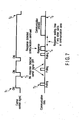
- FIG. 1 is a block diagram schematically showing a structure of a wireless communication device 1 according to the first embodiment of the present invention.
- the wireless communication device 1 includes a host device 2 and a reader/writer 4 that are connected to each other via wire or wirelessly.
- the feature of this embodiment is that the reader/writer 4 has a single antenna 11.
- the host device 2 of the wireless communication device 1 transmits various types of command data regarding signal transmission to the reader/writer 4, and receives a response result from a non-contact IC card 6 (to be referred to simply as IC card 6 hereinafter), that is, a communication object, via the reader/writer 4.
- IC card 6 to be referred to simply as IC card 6 hereinafter
- the reader/writer 4 includes a single antenna 11 designed to carry out wireless communication between the device and the IC card 6 located within the communication ready area. Further, the reader/writer 4 includes a signal transmission circuit 16 that functions as a carrier wave transmitting unit and command signal transmitting unit of the present invention, a signal receiving circuit 17 that functions as a signal receiving unit of the present invention and a control circuit 18 that functions as a carrier wave control unit of the present invention.
- the signal transmitting circuit 16 includes a carrier signal transmitting circuit 12, a modulation circuit 13 and a signal transmitting driver 14.
- the carrier signal transmitting circuit 12 of the signal transmitting circuit 16 serves to transmit a carrier signal (carrier wave) for making the LSI (not shown) equipped in the IC card 6 to generate electric power.
- the modulation circuit 13 serves to modulate the carrier signal based on command data transmitted from the host device 2 via the control circuit 18.
- the signal transmitting driver 14 serves to transmit the carrier signal that carries the command data as described above, via the antenna 11. It should be noted that the carrier signal transmitting circuit 12 transmits the carrier signal or stops the transmission of the signal in accordance with a command of transmission of a carrier signal or of stopping the transmission, supplied from the control circuit 18.
- the signal receiving circuit 17 serves to receive via the antenna 11 a response signal transmitted back from an IC card 6 that has responded to the carrier signal, demodulate the response signal and transfer the demodulated signal as a response result to the control circuit 18. Then, the control circuit 18 transfer data regarding the demodulated response result back to the host device 2. It should be noted that the control circuit 18 transmit a command for periodically set the carrier signal outputted from the carrier signal transmitting circuit 12 temporarily in an OFF state.
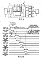
- FIG. 2 is a timing chart that indicates the timing of the temporary OFF control of the above-described control circuit 18 on the carrier signal.
- FIG. 3 shows a flowchart designed to describe the temporary OFF operation of the carrier signal, carried out by the control circuit 18.
- the control circuit 18 sets the carrier control signal to be transmitted to the transmitting circuit 16 to an ON state (Step 2), and makes the transmitting circuit 16 to output the carrier signal that carries the command data from the host device 2 (Timing 1 in FIG. 2 ).
- the control circuit 18 After waiting for the time period defined by the IC card 6, which is taken from the reception of the carrier signal to the time when the polling command becomes acceptable, the control circuit 18 outputs a polling command (Timing 2, Step 3). This polling command is outputted via the antenna 11 as it is carried on a carrier signal.
- the control circuit 18 sets a timer (not shown) to wait for a response from an IC card 6 located in a communication ready area created by the antenna 11 as the base point (Step 4), and waits for a preset time (Steps 5 and 6).
- the control circuit 18 controls the transmitting circuit 16 to temporarily set the carrier signal only for a very short period of time to an OFF state (Timing 3, Step 7).
- the control circuit 18 executes the communication process from that step onwards without temporarily setting the carrier signal to the OFF state (Step 8). Then, after the communication process is properly completed (Timing 5, YES in Step 9), the control circuit 18 sets the carrier signal to the OFF state (Timing 6, Step 7). If the communication process is not properly completed (NO in Step 9), the control circuit 18 displays an error message via a display unit that is not shown in the figure (Step 10).
- control circuit 18 sets the carrier signal to the OFF state in the process of the above-mentioned Step 7, and waits only for a very short period of time. After that, the operation of the control circuit 18 returns to the process of Step 2, where the carrier signal is once again outputted, and the processing steps described above that are carried out onto the other IC card 6 from this step onwards are repeated.
- the wireless communication device 1 operates in the following manner. That is, if a response from an IC card 6 to a polling command from the reader/writer 4 results in failure for some reason, the carrier signal is controlled to be temporarily in an OFF state at the above-described timing. Therefore, if the IC card 6 fails to response to the polling command, the sharp rise of the voltage for generating electric power in the LSI of the IC card 6 can be established, thereby making possible to have the IC card 6 power-on reset without fail. Consequently, it is possible to establish a good communication state between the reader/writer 4 and the IC card 6.
- FIG. 7 is a timing chart that indicates the timing of the temporary OFF operation of the carrier signal in the case where a plurality of IC cards 6 are processed at the same time.
- FIG. 8 is a timing chart that indicates the timing of the temporary OFF operation of the carrier signal in the case shown in FIG. 7 .
- the operation of the wireless communication device 1 shown in FIG. 1 where a plurality of IC cards 6 are processed at the same time will now be described.
- the control circuit 18 sets the carrier control signal to an ON state (Step 2), and makes the transmitting circuit 16 to output the carrier signal that carries the command data from the host device 2 (Timing 1 in FIG. 7 ). Then, the polling command is outputted via the antenna 11 (Timing 2, Step 3).
- the control circuit 18 sets a timer (Step 4) and waits for a response from an IC card 6 for a preset time (Steps 5 and 6).
- the carrier signal is temporarily set to the OFF state only for a very short period of time (Timing 3, Step 7).
- the control circuit 18 waits for a response from some other IC card 6 only for a predetermined waiting time (Steps 8 and 9).
- the communication process for the first IC card 6 is executed (Step 10).
- the control circuit 18 executes the communication process for the first IC card 6 (Step 11), and after that, executes the communication process for the second IC card 6 (Step 12).
- the control circuit 18 sets the carrier signal to an OFF state (Timing 6, Step 7). If the communication process is not properly completed for at least one of the IC cards 6 located within the communication ready area (NO in Step 13), the control circuit 18 displays an error message via a display unit that is not shown in the figure (Step 14).
- control circuit 18 sets the carrier signal to the OFF state in the process of the above-mentioned Step 7, and waits only for a present very short period of time. After that, the operation of the control circuit 18 returns to the process of Step 2, where the carrier signal is once again outputted, and the processing steps described above that are carried out onto the another IC card 6 from this step onwards are repeated.
- the communication process can be properly carried out for all of the IC cards 6.
- the wireless communication device 20 is characterized by including a plurality of antennas. It should be noted that those structural elements whose functions are similar to those of the wireless communication device 1 of the first embodiment described above will be designated by the same reference numerals respectively and the descriptions for the detailed structures and functions thereof will not be repeated.
- the wireless communication device 20 of this embodiment is different from the wireless communication device 1 of the first embodiment described above in the respect that a reader/writer 4 includes four antennas 21, 22, 23 and 24 for wirelessly communicating with an IC card 6, and a switching unit 25 that serves to switch over these four antennas. Further, the switching unit 25 includes a plurality of reply switches, though not shown in the figure, which correspond to the antennas 21 to 24, respectively. The switching unit 25 is connected to the control circuit 18 and these relay switches are switched over in accordance with the command supplied from the control circuit 18.
- the control circuit 18 selects, for example, the antenna 21 and sets the switch signal of the corresponding relay switch to the ON state (Timing T1 in FIG. 10 ). Subsequently, the control circuit 18 controls the signal transmitting circuit 16 to output a carrier signal via the selected antenna 21 (Timing T2).
- the control circuit 18 controls the signal transmitting circuit 16 to transmit a polling command via the antenna 21 (Timing T3) and sets the timer to wait for a response from an IC card 6. In the case where there is no response from an IC card 6 within the preset time-out period, the control circuit 18 controls the transmitting circuit 16 to deactivate the carrier signal (Timing T4), and then control the switching unit 25 to switch the relay switch to change the antenna 21 to the antenna 22 (Timing T5).
- control circuit 18 outputs a carrier signal that carries a polling command via the next antenna 22.
- the antenna is further switched to the next one, antenna 23.
- the control circuit 18 repeats the above-described switching operation until a response is received from an IC card 6 (Timing T6). Then, in the case where there is a response from an IC card 6, the control circuit 18 executes the communication process without setting the carrier signal to the OFF state or switching the antenna to another.
- FIG. 10 illustrates the case where a response is received from an IC card 6 when the antenna 21 is switched over to antenna 22, 23 and 24 and then further switched back to the antenna 21.
- the carrier signal can be controlled in a temporary OFF manner.
- the antennas are switched over while the connection state of the relay switches of the switching unit 25 is released. In this manner, it is possible to prevent the load from being applied to the contact point of each relay switch, and therefore the lifetime of the relay switch can be prolonged. Consequently, a highly reliable communication process can be performed.
- non-contact IC cards 6 are applied as communication objects; however the present invention is not limited to the case, but it can be applied to communications with some other object such as wireless tag.
- the control circuit 18 of the reader/writer 4 controls the carrier signal to be temporarily set to the OFF state and then back to the ON state periodically at a predetermined timing. In this manner, if the establishment of the communication with an IC card 6 results in failure, the power-on-reset function can be properly operated.
- the present invention is not limited to this operation, but it is alternatively possible to temporarily lower the carrier signal to a certain level periodically. In this.case, the certain level indicates such a level lower than the threshold of the carrier signal where it is possible to make an IC card 6 to generate the electric power for communication.
Description
- The present invention relates to a wireless communication device that performs wireless communications between itself and an object of communication such as non-contact IC card, and carries out various types of data processing.
- Conventionally, an antenna device having the following structure is known as a wireless communication device. That is, two sets of antenna assembly members each having a plurality of loop antennas placed in the same plane are arranged to face each other while interposing therebetween a passage where communication objects such as wireless tags pass through. (See, for example,
Jpn. Pat. Appln. KOKAI Publication No. 2002-237720 FIG. 1 ).) The characteristics of this antenna device are that some of these loop antennas are periodically switched to invert the phases and thus the non-detectible region where a wireless tag is not detected is minimized. It should be noted that the antenna device of this type is utilized as, for example, a gate for preventing shoplifting. - The conventional type of antenna device described above, however, entails the following drawbacks. That is, while an object equipped with a wireless tag passing through between a pair of antenna assembly members, if the wireless tag enters the communication ready area of the antenna device at a relatively low speed, the rise of the voltage generated inside the wireless tag becomes gentle and therefore the power-on-reset function of the wireless tag does not operate properly in some cases. In these case, the communication between the antenna device and the wireless tag is not established, and therefore the reliability of the antenna device is lowered.
- Meanwhile, in the case where the phase of particular loop antennas are periodically inverted as in the above-described antenna device, the relay switch and the like need be operated for phase inversion while transmitting carrier waves for communication from the loop antennas. Thus, the switch is operated a number of times while the connection state is on, and therefore the contact point of the switch is caused to labor, thereby shortening the lifetime of the contact point.
-
US 5 519 729 discloses a wireless communication device according to the preamble ofclaim 1. - The object of the present invention is to provide a highly reliable wireless communication device that can establish a good communication state between the device itself and an communication object regardless of the status of the communication object.
- This is achieved by the present invention as defined in
claim 1. - Further advantageous embodiments are defined in the sub-claims.
- The invention can be more fully understood from the following detailed description when taken in conjunction with the accompanying drawings, in which:
-
FIG. 1 is a block diagram showing a brief structure of a wireless communication device according to the first embodiment of the present invention; -
FIG. 2 is a timing chart that indicates the timing of the temporary OFF operation of the carrier signal in the device shown inFIG. 1 ; -
FIG. 3 is a flowchart for explain the temporary OFF operation of the carrier signal together withFIG. 2 ; -
FIG. 4 is a diagram showing a state in which an IC card enters a communication ready area created by the antenna of the device shown inFIG. 1 , serving as the base point; -
FIG. 5 is a timing chart that indicates the relationship between the change in the voltage generated in the IC card and the power-on-reset signal when the IC card is made to enter the communication ready area at a relatively high speed in the state shown inFIG. 4 ; -
FIG. 6 is a timing chart that indicates the relationship between the change in the voltage generated in the IC card and the power-on-reset signal when the IC card is made to enter the communication ready area at a relatively high speed in the case where the present invention is applied; -
FIG. 7 is a timing chart that indicates the timing of the temporary OFF operation of the carrier signal in the case where a plurality of IC cards are processed by the device shown inFIG. 1 ; -
FIG. 8 is a flowchart for explain the temporary OFF operation of the carrier signal together withFIG. 7 ; -
FIG. 9 is a block diagram showing a brief structure of a wireless communication device according to the second embodiment of the present invention; and -
FIG. 10 is a timing chart that indicates the relationship between the timing for switching the antenna and the timing of the temporary OFF operation of the carrier signal in the device shown inFIG. 9 . - Embodiments of the present invention will now be described in detail with reference to accompanying drawings.
-
FIG. 1 is a block diagram schematically showing a structure of awireless communication device 1 according to the first embodiment of the present invention. As shown in the figure, thewireless communication device 1 includes ahost device 2 and a reader/writer 4 that are connected to each other via wire or wirelessly. The feature of this embodiment is that the reader/writer 4 has asingle antenna 11. - The
host device 2 of thewireless communication device 1 transmits various types of command data regarding signal transmission to the reader/writer 4, and receives a response result from a non-contact IC card 6 (to be referred to simply asIC card 6 hereinafter), that is, a communication object, via the reader/writer 4. - The reader/
writer 4 includes asingle antenna 11 designed to carry out wireless communication between the device and theIC card 6 located within the communication ready area. Further, the reader/writer 4 includes asignal transmission circuit 16 that functions as a carrier wave transmitting unit and command signal transmitting unit of the present invention, asignal receiving circuit 17 that functions as a signal receiving unit of the present invention and acontrol circuit 18 that functions as a carrier wave control unit of the present invention. Thesignal transmitting circuit 16 includes a carriersignal transmitting circuit 12, amodulation circuit 13 and asignal transmitting driver 14. - The carrier
signal transmitting circuit 12 of thesignal transmitting circuit 16 serves to transmit a carrier signal (carrier wave) for making the LSI (not shown) equipped in theIC card 6 to generate electric power. Themodulation circuit 13 serves to modulate the carrier signal based on command data transmitted from thehost device 2 via thecontrol circuit 18. Then, thesignal transmitting driver 14 serves to transmit the carrier signal that carries the command data as described above, via theantenna 11. It should be noted that the carriersignal transmitting circuit 12 transmits the carrier signal or stops the transmission of the signal in accordance with a command of transmission of a carrier signal or of stopping the transmission, supplied from thecontrol circuit 18. - The
signal receiving circuit 17 serves to receive via the antenna 11 a response signal transmitted back from anIC card 6 that has responded to the carrier signal, demodulate the response signal and transfer the demodulated signal as a response result to thecontrol circuit 18. Then, thecontrol circuit 18 transfer data regarding the demodulated response result back to thehost device 2. It should be noted that thecontrol circuit 18 transmit a command for periodically set the carrier signal outputted from the carriersignal transmitting circuit 12 temporarily in an OFF state. - The operation of the
wireless communication device 1 that has the above-described structure will now be described with reference toFIGS. 2 and3 .FIG. 2 is a timing chart that indicates the timing of the temporary OFF control of the above-describedcontrol circuit 18 on the carrier signal. Further,FIG. 3 shows a flowchart designed to describe the temporary OFF operation of the carrier signal, carried out by thecontrol circuit 18. - As shown, when a polling command outputted from the
host device 2 is received by the reader/writer 4 (Step 1 inFIG. 3 ), thecontrol circuit 18 sets the carrier control signal to be transmitted to the transmittingcircuit 16 to an ON state (Step 2), and makes the transmittingcircuit 16 to output the carrier signal that carries the command data from the host device 2 (Timing 1 inFIG. 2 ). - In the meantime, after waiting for the time period defined by the
IC card 6, which is taken from the reception of the carrier signal to the time when the polling command becomes acceptable, thecontrol circuit 18 outputs a polling command (Timing 2, Step 3). This polling command is outputted via theantenna 11 as it is carried on a carrier signal. - Then, the
control circuit 18 sets a timer (not shown) to wait for a response from anIC card 6 located in a communication ready area created by theantenna 11 as the base point (Step 4), and waits for a preset time (Steps 5 and 6). Here, under a condition where thesignal receiving circuit 17 does not receive the response signal from anyIC card 6 within the preset time period (that is, NO inStep 5 and YES in Step 6), thecontrol circuit 18 controls the transmittingcircuit 16 to temporarily set the carrier signal only for a very short period of time to an OFF state (Timing 3, Step 7). - On the other hand, under a condition where the
signal receiving circuit 17 receives the response signal from anIC card 6 within the preset time period after outputting the polling command (that is,Timing 4 and YES in Step 5), thecontrol circuit 18 executes the communication process from that step onwards without temporarily setting the carrier signal to the OFF state (Step 8). Then, after the communication process is properly completed (Timing 5, YES in Step 9), thecontrol circuit 18 sets the carrier signal to the OFF state (Timing 6, Step 7). If the communication process is not properly completed (NO in Step 9), thecontrol circuit 18 displays an error message via a display unit that is not shown in the figure (Step 10). - Then, the
control circuit 18 sets the carrier signal to the OFF state in the process of the above-mentionedStep 7, and waits only for a very short period of time. After that, the operation of thecontrol circuit 18 returns to the process ofStep 2, where the carrier signal is once again outputted, and the processing steps described above that are carried out onto theother IC card 6 from this step onwards are repeated. - As described above, the
wireless communication device 1 according to this embodiment operates in the following manner. That is, if a response from anIC card 6 to a polling command from the reader/writer 4 results in failure for some reason, the carrier signal is controlled to be temporarily in an OFF state at the above-described timing. Therefore, if theIC card 6 fails to response to the polling command, the sharp rise of the voltage for generating electric power in the LSI of theIC card 6 can be established, thereby making possible to have theIC card 6 power-on reset without fail. Consequently, it is possible to establish a good communication state between the reader/writer 4 and theIC card 6. - In other words, while an
IC card 6 passing through a communication ready area created by theantenna 11 of the reader/writer 4, which serves as the base point as shown inFIG. 4 , if theIC card 6 is made to enter the area at a normal speed, the rise of the voltage generated in the LSI of theIC card 6 becomes sharp as shown inFIG. 5 and therefore the power-on-reset function of the IC card can operate properly. In contrast, if theIC card 6 is made to enter the area at a relative low speed, the rise of the voltage generated in the LSI becomes gentle as shown inFIG. 6 and therefore the power-on-reset function of theIC card 6 cannot operate properly in some cases. In these cases, such a state that theIC card 6 fails to make a response is created, and consequently, the connection is not established. However, by controlling the carrier signal in a temporary OFF manner periodically as in the above-described embodiment, the rise of the voltage in the LSI can be made sharp, thereby enabling the power-on-reset function to operate properly. Thus, a good communication state can be established between theIC card 6 and the reader/writer 4. - Next, a remodeled version of the first embodiment provided above will now be described with reference to
FIGS. 7 and8 together withFIG. 1 .FIG. 7 is a timing chart that indicates the timing of the temporary OFF operation of the carrier signal in the case where a plurality ofIC cards 6 are processed at the same time. Further,FIG. 8 is a timing chart that indicates the timing of the temporary OFF operation of the carrier signal in the case shown inFIG. 7 . In other words, the operation of thewireless communication device 1 shown inFIG. 1 where a plurality ofIC cards 6 are processed at the same time will now be described. - As shown, when a polling command outputted from the
host device 2 is received (Step 1 inFIG. 8 ), thecontrol circuit 18 sets the carrier control signal to an ON state (Step 2), and makes the transmittingcircuit 16 to output the carrier signal that carries the command data from the host device 2 (Timing 1 inFIG. 7 ). Then, the polling command is outputted via the antenna 11 (Timing 2, Step 3). - Then, the
control circuit 18 sets a timer (Step 4) and waits for a response from anIC card 6 for a preset time (Steps 5 and 6). Here, in the case where the response signal from theIC card 6 is not received within the preset time period (that is, NO inStep 5 and YES in Step 6), the carrier signal is temporarily set to the OFF state only for a very short period of time (Timing 3, Step 7). - On the other hand, in the case where the response signal is received from the
IC card 6 within the preset time period (that is,Timing 4 and YES in Step 5), thecontrol circuit 18 waits for a response from someother IC card 6 only for a predetermined waiting time (Steps 8 and 9). In the case where the response signal from theother IC card 6 is not received within the preset time period (that is, NO inStep 8 and YES in Step 9), the communication process for thefirst IC card 6 is executed (Step 10). - In the case where the response signal from the
other IC card 6 is received within the preset time period (that is, YES in Step 8), thecontrol circuit 18 executes the communication process for the first IC card 6 (Step 11), and after that, executes the communication process for the second IC card 6 (Step 12). - Then, after the communication process is properly completed for each one of the
IC cards 6 located in a communication ready area of the antenna 11 (Timing 5, YES in Step 13), thecontrol circuit 18 sets the carrier signal to an OFF state (Timing 6, Step 7). If the communication process is not properly completed for at least one of theIC cards 6 located within the communication ready area (NO in Step 13), thecontrol circuit 18 displays an error message via a display unit that is not shown in the figure (Step 14). - Then, the
control circuit 18 sets the carrier signal to the OFF state in the process of the above-mentionedStep 7, and waits only for a present very short period of time. After that, the operation of thecontrol circuit 18 returns to the process ofStep 2, where the carrier signal is once again outputted, and the processing steps described above that are carried out onto the anotherIC card 6 from this step onwards are repeated. - As described above, according to the remodeled version of the embodiment, if a plurality of
IC cards 6 enter the communication ready area of theantenna 11 of thewireless communication device 1, the communication process can be properly carried out for all of theIC cards 6. - Next, a
wireless communication device 20 according to the second embodiment of the present invention will now be described with reference toFIGS. 9 and 10 . Thewireless communication device 20 is characterized by including a plurality of antennas. It should be noted that those structural elements whose functions are similar to those of thewireless communication device 1 of the first embodiment described above will be designated by the same reference numerals respectively and the descriptions for the detailed structures and functions thereof will not be repeated. - As can be seen in
FIG. 9 , thewireless communication device 20 of this embodiment is different from thewireless communication device 1 of the first embodiment described above in the respect that a reader/writer 4 includes fourantennas IC card 6, and aswitching unit 25 that serves to switch over these four antennas. Further, the switchingunit 25 includes a plurality of reply switches, though not shown in the figure, which correspond to theantennas 21 to 24, respectively. The switchingunit 25 is connected to thecontrol circuit 18 and these relay switches are switched over in accordance with the command supplied from thecontrol circuit 18. - With the above-described structure, when the reader/
writer 4 receives a polling command from thehost device 2, thecontrol circuit 18 selects, for example, theantenna 21 and sets the switch signal of the corresponding relay switch to the ON state (Timing T1 inFIG. 10 ). Subsequently, thecontrol circuit 18 controls thesignal transmitting circuit 16 to output a carrier signal via the selected antenna 21 (Timing T2). - After that, the
control circuit 18 controls thesignal transmitting circuit 16 to transmit a polling command via the antenna 21 (Timing T3) and sets the timer to wait for a response from anIC card 6. In the case where there is no response from anIC card 6 within the preset time-out period, thecontrol circuit 18 controls the transmittingcircuit 16 to deactivate the carrier signal (Timing T4), and then control the switchingunit 25 to switch the relay switch to change theantenna 21 to the antenna 22 (Timing T5). - Subsequently, in a similar manner to the above, the
control circuit 18 outputs a carrier signal that carries a polling command via thenext antenna 22. - In the case where there is no response to the polling command received from an
IC card 6, the antenna is further switched to the next one,antenna 23. In this manner, thecontrol circuit 18 repeats the above-described switching operation until a response is received from an IC card 6 (Timing T6). Then, in the case where there is a response from anIC card 6, thecontrol circuit 18 executes the communication process without setting the carrier signal to the OFF state or switching the antenna to another. It should be noted that the example shown inFIG. 10 illustrates the case where a response is received from anIC card 6 when theantenna 21 is switched over toantenna antenna 21. - As described above, according to this embodiment, each time the antenna is switched to another, the carrier signal can be controlled in a temporary OFF manner. With this structure, as in the case of the first embodiment described above, even if an
IC card 6 once fails to make a response, the power-on-reset function can be properly operated, thereby making it possible to establish a good communication state. - Further, according to this embodiment, the antennas are switched over while the connection state of the relay switches of the switching
unit 25 is released. In this manner, it is possible to prevent the load from being applied to the contact point of each relay switch, and therefore the lifetime of the relay switch can be prolonged. Consequently, a highly reliable communication process can be performed. - The above-described embodiments are described in connection with the case where
non-contact IC cards 6 are applied as communication objects; however the present invention is not limited to the case, but it can be applied to communications with some other object such as wireless tag. - In addition, in the embodiments described above; the
control circuit 18 of the reader/writer 4 controls the carrier signal to be temporarily set to the OFF state and then back to the ON state periodically at a predetermined timing. In this manner, if the establishment of the communication with anIC card 6 results in failure, the power-on-reset function can be properly operated. However, the present invention is not limited to this operation, but it is alternatively possible to temporarily lower the carrier signal to a certain level periodically. In this.case, the certain level indicates such a level lower than the threshold of the carrier signal where it is possible to make anIC card 6 to generate the electric power for communication.
Claims (7)
- A wireless communication device comprising
an antenna (11) configured to carry out wireless communication with a communication object (6),
a carrier wave transmitting unit (16) configured to transmit via the antenna (11) a carrier wave to a communication object (6) located within range of the antenna (11), the carrier wave serving to render the communication object (6) to generate electric power for the communication, and
a signal receiving unit (17) configured to receive via the antenna (11) a response signal transmitted in reply to the carrier wave from the communication object (6),
characterized by
a carrier wave control unit (18) configured to periodically control the carrier wave transmitted from the carrier wave transmitting unit in a temporary off state when the signal receiving unit does not receive the response signal within a certain period of time after the carrier wave transmitting unit (16) has transmitted the carrier wave, wherein the duration of the temporary off state is short in comparison to the period of the periodic controlling. - The wireless communication device according to claim 1, further comprising a command transmitting unit (16) configured to transmit command data to the communication object (6),
characterized in that the carrier wave control unit (18) temporarily sets the carrier wave to the OFF state each time a polling command is transmitted from the command transmitting unit. - The wireless communication device according to claim 2, wherein
the command transmitting unit (16) is configured to transmit command data to the communication object (6) carried on the carrier wave, and
characterized in that the carrier wave control unit (18) temporarily sets the carrier wave to the OFF state when the signal receiving unit does not receive the response signal within a certain period of time after the command transmitting unit transmits the polling command carried on the carrier wave. - The wireless communication device according to any of claims 1-3, wherein the antenna comprises a plurality of antennas (21, 22, 23, 24) configured to carry out wireless communication with the communication object (6), the device further comprising
a switching unit (25) configured to switch between the plurality of antennas, and wherein
the carrier wave transmitting unit (16) is configured to transmit via the switched-on antenna the carrier wave to the communication object located within range of the switched-on antenna. - The wireless communication device according to claim 4, characterized in that the switching unit (25) switches between the plurality of antennas (21, 22, 23, 24) while the carrier wave control unit (18) is setting the carrier wave to the OFF state.
- The wireless communication device according to claim 4, characterized in that the carrier wave control unit (18) controls the carrier wave in a temporary off state each time the switching unit (25) switches between the plurality of antennas (21, 22, 23, 24).
- The wireless communication device according to any of claims 1-6, wherein the carrier wave control unit (18) is configured to set the level of the carrier wave transmitted from the carrier wave transmitting unit below a threshold level in the temporary off state.
Applications Claiming Priority (2)
| Application Number | Priority Date | Filing Date | Title |
|---|---|---|---|
| JP2004026619 | 2004-02-03 | ||
| JP2004026619A JP4519476B2 (en) | 2004-02-03 | 2004-02-03 | Wireless communication device |
Publications (3)
| Publication Number | Publication Date |
|---|---|
| EP1562133A2 EP1562133A2 (en) | 2005-08-10 |
| EP1562133A3 EP1562133A3 (en) | 2009-11-04 |
| EP1562133B1 true EP1562133B1 (en) | 2010-05-19 |
Family
ID=34675469
Family Applications (1)
| Application Number | Title | Priority Date | Filing Date |
|---|---|---|---|
| EP04029886A Active EP1562133B1 (en) | 2004-02-03 | 2004-12-16 | Wireless communication device |
Country Status (5)
| Country | Link |
|---|---|
| US (1) | US7515925B2 (en) |
| EP (1) | EP1562133B1 (en) |
| JP (1) | JP4519476B2 (en) |
| CN (1) | CN1652136A (en) |
| DE (1) | DE602004027209D1 (en) |
Families Citing this family (15)
| Publication number | Priority date | Publication date | Assignee | Title |
|---|---|---|---|---|
| JP2005117153A (en) * | 2003-10-03 | 2005-04-28 | Toshiba Corp | Wireless communication apparatus, wireless communication method, and wireless communication medium |
| WO2007026291A2 (en) * | 2005-09-02 | 2007-03-08 | Nxp B.V. | Data carrier with a radio frequency interface |
| JP5071016B2 (en) * | 2006-10-23 | 2012-11-14 | 富士通株式会社 | RFID tag response control method, RFID system, RFID tag, response control information generation program, and response control program |
| EP2020641B1 (en) | 2007-08-02 | 2013-09-11 | Brother Kogyo Kabushiki Kaisha | RFID tag information communicating apparatus |
| JP5019173B2 (en) * | 2007-08-02 | 2012-09-05 | ブラザー工業株式会社 | Wireless tag information communication device |
| EP2164023B1 (en) * | 2008-09-11 | 2017-05-17 | Rockwell Automation Germany GmbH & Co. KG | Enhanced RFID output control |
| EP2166485B1 (en) | 2008-09-19 | 2016-02-24 | Rockwell Automation Germany GmbH & Co. KG | RFID Reaction time reduction |
| US20100188251A1 (en) * | 2009-01-23 | 2010-07-29 | Panuce Donald G | Apparatus and method for an ac wireless switch |
| JP4854776B2 (en) * | 2009-09-15 | 2012-01-18 | 東芝テック株式会社 | RF tag reader / writer |
| JP2012023565A (en) * | 2010-07-14 | 2012-02-02 | Sony Corp | Communication system and communication device |
| JP5889595B2 (en) * | 2011-10-14 | 2016-03-22 | Jr東日本メカトロニクス株式会社 | System, main reader / writer device, information processing method, and program |
| JP2017063275A (en) * | 2015-09-24 | 2017-03-30 | 株式会社タニタ | Radio communication device, radio communication system, and method for controlling phase switching of supply current to antenna |
| JP2018022428A (en) * | 2016-08-05 | 2018-02-08 | 東芝テック株式会社 | RFID tag reading device and program |
| US10862543B2 (en) * | 2019-01-17 | 2020-12-08 | Capital One Services, Llc | Apparatus and method for wireless communication with improved reliability |
| CN112716760A (en) * | 2020-12-22 | 2021-04-30 | 未来穿戴技术有限公司 | Connection method of massage instrument, massage instrument and terminal equipment |
Family Cites Families (38)
| Publication number | Priority date | Publication date | Assignee | Title |
|---|---|---|---|---|
| US4029945A (en) * | 1975-08-27 | 1977-06-14 | Stanley Electric Co., Ltd. | Card and card reader apparatus therefor |
| US4797541A (en) * | 1986-04-14 | 1989-01-10 | American Telephone and Telegraph Company--AT&T Information Systems | Power regulator for a contactless credit card system |
| US4795898A (en) * | 1986-04-28 | 1989-01-03 | American Telephone And Telegraph Company | Personal memory card having a contactless interface using differential data transfer |
| JP2597623B2 (en) * | 1987-10-08 | 1997-04-09 | 株式会社トキメック | Power supply method by electromagnetic induction coupling |
| JPH01184781A (en) * | 1988-01-18 | 1989-07-24 | Tokyo Keiki Co Ltd | Memory package system |
| US5070500A (en) * | 1988-08-30 | 1991-12-03 | Tokyo Keiki Company Ltd. | Memory package system utilizing inductive coupling between memory module and read/write unit |
| GB2229845B (en) * | 1989-04-01 | 1993-08-04 | Avery Ltd W & T | Transaction system |
| JPH0528330A (en) * | 1991-07-24 | 1993-02-05 | Mitsubishi Electric Corp | Non-contact type portable carrier and its initializing method |
| US5519729A (en) * | 1992-03-31 | 1996-05-21 | Micro-Sensys Gmbh | Method of and device for transmitting serial data structures in systems for identifying information carriers |
| US5354975A (en) * | 1992-07-01 | 1994-10-11 | Tokimec Inc. | Contactless data processing apparatus |
| US5450088A (en) * | 1992-11-25 | 1995-09-12 | Texas Instruments Deutschland Gmbh | Transponder arrangement |
| JP3201157B2 (en) | 1994-07-26 | 2001-08-20 | 松下電器産業株式会社 | IC card device |
| JPH0844833A (en) * | 1994-08-03 | 1996-02-16 | Mitsubishi Denki Semiconductor Software Kk | Reader/writer for non-contact ic card and reader/writer system for non-contact ic card |
| JP2866016B2 (en) * | 1994-12-22 | 1999-03-08 | 三菱電機株式会社 | Modulator for IC card read / write device and demodulator thereof |
| JP3360002B2 (en) * | 1996-03-14 | 2002-12-24 | 沖電気工業株式会社 | Contact / non-contact IC card and contact / non-contact IC card reader / writer |
| FR2752076B1 (en) * | 1996-08-05 | 1998-09-11 | Inside Technologies | ELECTRICAL SUPPLY SYSTEM FOR MICROCIRCUIT WITH MIXED OPERATION, WITH OR WITHOUT CONTACT |
| JPH10285086A (en) * | 1997-04-02 | 1998-10-23 | Omron Corp | Transmitting and receiving device and system |
| US5905372A (en) * | 1997-12-17 | 1999-05-18 | Motorola, Inc. | Apparatus and method for delivering power to a contactless portable data device |
| US6404325B1 (en) | 1998-01-08 | 2002-06-11 | Intermec Ip Corp. | Method and system for storage and recovery of vital information on radio frequency transponders |
| JPH11205334A (en) * | 1998-01-16 | 1999-07-30 | Mitsubishi Electric Corp | Recognition system and recognition method for contactless ic card |
| ATE259513T1 (en) * | 1998-03-27 | 2004-02-15 | Koninkl Philips Electronics Nv | CIRCUIT FOR DATA CARRIERS TO REDUCE POWER CONSUMPTION |
| JP3589029B2 (en) * | 1998-05-27 | 2004-11-17 | 松下電器産業株式会社 | Reader / writer, non-contact IC card and card system using them |
| JP4357036B2 (en) * | 1999-08-06 | 2009-11-04 | 株式会社トーエネック | Antenna switching system |
| JP2001250089A (en) * | 2000-03-07 | 2001-09-14 | Tamura Electric Works Ltd | Non-contact ic card reader/writer |
| US6472065B1 (en) * | 2000-07-13 | 2002-10-29 | 3M Innovative Properties Company | Clear adhesive sheet |
| AU2001262739A1 (en) * | 2000-08-15 | 2002-02-25 | Omron Corporation | Noncontact communication medium and noncontact communication system |
| JP3607585B2 (en) * | 2000-08-23 | 2005-01-05 | 日本電信電話株式会社 | Non-contact response device |
| JP4822588B2 (en) * | 2001-02-08 | 2011-11-24 | 富士通セミコンダクター株式会社 | Information processing apparatus and information processing device |
| JP3498716B2 (en) | 2001-02-09 | 2004-02-16 | オムロン株式会社 | Antenna device |
| US6727803B2 (en) | 2001-03-16 | 2004-04-27 | E-Tag Systems, Inc. | Method and apparatus for efficiently querying and identifying multiple items on a communication channel |
| JP2002352198A (en) * | 2001-05-25 | 2002-12-06 | Nippon Signal Co Ltd:The | Non-contact ic card reader/writer |
| GB2377341A (en) | 2001-06-01 | 2003-01-08 | George L Powell | Signal sampling to reduce noise effects in an identification system |
| JP3904859B2 (en) * | 2001-07-30 | 2007-04-11 | シャープ株式会社 | Power-on reset circuit and IC card having the same |
| JP4727860B2 (en) * | 2001-08-03 | 2011-07-20 | 富士通株式会社 | Wireless operation device and program |
| FR2829853B1 (en) * | 2001-09-14 | 2004-01-02 | A S K | MODULATOR FOR ELECTROMAGNETIC SIGNALS TRANSMITTED BY A CONTACTLESS TRANSMISSION / RECEPTION SYSTEM |
| MXPA04006667A (en) * | 2002-01-09 | 2005-05-27 | Meadwestvaco Corp | Intelligent station using multiple rf antennae and inventory control system and method incorporating same. |
| JP2003296665A (en) * | 2002-03-29 | 2003-10-17 | Takamisawa Cybernetics Co Ltd | Ic reader-writer and control method for ic reader-writer |
| US7019639B2 (en) * | 2003-02-03 | 2006-03-28 | Ingrid, Inc. | RFID based security network |
-
2004
- 2004-02-03 JP JP2004026619A patent/JP4519476B2/en not_active Expired - Lifetime
- 2004-12-16 DE DE602004027209T patent/DE602004027209D1/en active Active
- 2004-12-16 EP EP04029886A patent/EP1562133B1/en active Active
- 2004-12-29 US US11/023,512 patent/US7515925B2/en active Active
-
2005
- 2005-02-02 CN CNA2005100078100A patent/CN1652136A/en active Pending
Also Published As
| Publication number | Publication date |
|---|---|
| EP1562133A2 (en) | 2005-08-10 |
| US7515925B2 (en) | 2009-04-07 |
| EP1562133A3 (en) | 2009-11-04 |
| US20050170793A1 (en) | 2005-08-04 |
| DE602004027209D1 (en) | 2010-07-01 |
| JP4519476B2 (en) | 2010-08-04 |
| CN1652136A (en) | 2005-08-10 |
| JP2005223401A (en) | 2005-08-18 |
Similar Documents
| Publication | Publication Date | Title |
|---|---|---|
| EP1562133B1 (en) | Wireless communication device | |
| EP1146475B1 (en) | Card reader/writer for non-contact IC card | |
| US10108383B2 (en) | Communication device communicating target data with external device according to near field communication | |
| EP1845631A1 (en) | Rfid communication control method and rfid system using the same | |
| JP2011044092A (en) | Communication system, information processing device, information processing method, and information processing program | |
| JP4496105B2 (en) | Wireless communication device | |
| EP1816705A1 (en) | Control system of an antenna array | |
| WO2006082612A1 (en) | Rfid carrier sense method and rfid system using the same | |
| US20130203355A1 (en) | Short-distance wireless communication device | |
| CN107426668B (en) | Communication device | |
| JP4321490B2 (en) | Non-contact communication system | |
| JP2004227315A (en) | Noncontact ic card reader/writer device | |
| US9311587B2 (en) | RFID device being operable in a first and second operating state | |
| JP4116273B2 (en) | Wireless card having random number generator, semiconductor device for the wireless card, and wireless card system using the wireless card | |
| US6067626A (en) | Method of processing externally supplied data by CPU in non-operating state and portable terminal device for the same | |
| JP2009010483A (en) | Radio tag reader-writer and its signal transmission/reception method | |
| JP3511925B2 (en) | Moving object identification device | |
| US11755876B2 (en) | Interference suppression apparatus and interference suppression system | |
| JP4407604B2 (en) | Communication device | |
| JP2001034720A (en) | Reader/writer for id tag | |
| WO2006030493A1 (en) | Non-contact type communication system | |
| JP2007179294A (en) | Ic card, and ic card program | |
| CN116781112A (en) | Communication method for near field communication device | |
| JP3427803B2 (en) | Electronic device operation mode changing system and electronic device | |
| CN111490805A (en) | NFC communication |
Legal Events
| Date | Code | Title | Description |
|---|---|---|---|
| PUAI | Public reference made under article 153(3) epc to a published international application that has entered the european phase |
Free format text: ORIGINAL CODE: 0009012 |
|
| 17P | Request for examination filed |
Effective date: 20041216 |
|
| AK | Designated contracting states |
Kind code of ref document: A2 Designated state(s): AT BE BG CH CY CZ DE DK EE ES FI FR GB GR HU IE IS IT LI LT LU MC NL PL PT RO SE SI SK TR |
|
| AX | Request for extension of the european patent |
Extension state: AL BA HR LV MK YU |
|
| PUAL | Search report despatched |
Free format text: ORIGINAL CODE: 0009013 |
|
| AK | Designated contracting states |
Kind code of ref document: A3 Designated state(s): AT BE BG CH CY CZ DE DK EE ES FI FR GB GR HU IE IS IT LI LT LU MC NL PL PT RO SE SI SK TR |
|
| AX | Request for extension of the european patent |
Extension state: AL BA HR LV MK YU |
|
| RIC1 | Information provided on ipc code assigned before grant |
Ipc: G06K 7/00 20060101AFI20050524BHEP Ipc: G06K 19/07 20060101ALI20051214BHEP |
|
| PUAF | Information related to the publication of a search report (a3 document) modified or deleted |
Free format text: ORIGINAL CODE: 0009199SEPU |
|
| D17D | Deferred search report published (deleted) | ||
| RIC1 | Information provided on ipc code assigned before grant |
Ipc: G06K 7/00 20060101AFI20050524BHEP |
|
| 17Q | First examination report despatched |
Effective date: 20061115 |
|
| GRAJ | Information related to disapproval of communication of intention to grant by the applicant or resumption of examination proceedings by the epo deleted |
Free format text: ORIGINAL CODE: EPIDOSDIGR1 |
|
| GRAP | Despatch of communication of intention to grant a patent |
Free format text: ORIGINAL CODE: EPIDOSNIGR1 |
|
| PUAL | Search report despatched |
Free format text: ORIGINAL CODE: 0009013 |
|
| GRAP | Despatch of communication of intention to grant a patent |
Free format text: ORIGINAL CODE: EPIDOSNIGR1 |
|
| AK | Designated contracting states |
Kind code of ref document: A3 Designated state(s): AT BE BG CH CY CZ DE DK EE ES FI FR GB GR HU IE IS IT LI LT LU MC NL PL PT RO SE SI SK TR |
|
| AX | Request for extension of the european patent |
Extension state: AL BA HR LV MK YU |
|
| GRAS | Grant fee paid |
Free format text: ORIGINAL CODE: EPIDOSNIGR3 |
|
| GRAA | (expected) grant |
Free format text: ORIGINAL CODE: 0009210 |
|
| AK | Designated contracting states |
Kind code of ref document: B1 Designated state(s): DE FR GB |
|
| REG | Reference to a national code |
Ref country code: GB Ref legal event code: FG4D |
|
| REF | Corresponds to: |
Ref document number: 602004027209 Country of ref document: DE Date of ref document: 20100701 Kind code of ref document: P |
|
| AKX | Designation fees paid |
Designated state(s): DE FR GB |
|
| PLBE | No opposition filed within time limit |
Free format text: ORIGINAL CODE: 0009261 |
|
| STAA | Information on the status of an ep patent application or granted ep patent |
Free format text: STATUS: NO OPPOSITION FILED WITHIN TIME LIMIT |
|
| 26N | No opposition filed |
Effective date: 20110222 |
|
| REG | Reference to a national code |
Ref country code: DE Ref legal event code: R097 Ref document number: 602004027209 Country of ref document: DE Effective date: 20110221 |
|
| REG | Reference to a national code |
Ref country code: FR Ref legal event code: PLFP Year of fee payment: 12 |
|
| REG | Reference to a national code |
Ref country code: FR Ref legal event code: PLFP Year of fee payment: 13 |
|
| REG | Reference to a national code |
Ref country code: FR Ref legal event code: PLFP Year of fee payment: 14 |
|
| PGFP | Annual fee paid to national office [announced via postgrant information from national office to epo] |
Ref country code: GB Payment date: 20231026 Year of fee payment: 20 |
|
| PGFP | Annual fee paid to national office [announced via postgrant information from national office to epo] |
Ref country code: FR Payment date: 20231009 Year of fee payment: 20 Ref country code: DE Payment date: 20231024 Year of fee payment: 20 |