EP1560321A2 - Power supply circuit and power supply control method therein - Google Patents
Power supply circuit and power supply control method therein Download PDFInfo
- Publication number
- EP1560321A2 EP1560321A2 EP04256963A EP04256963A EP1560321A2 EP 1560321 A2 EP1560321 A2 EP 1560321A2 EP 04256963 A EP04256963 A EP 04256963A EP 04256963 A EP04256963 A EP 04256963A EP 1560321 A2 EP1560321 A2 EP 1560321A2
- Authority
- EP
- European Patent Office
- Prior art keywords
- load
- power supply
- coil
- circuit
- transistor
- Prior art date
- Legal status (The legal status is an assumption and is not a legal conclusion. Google has not performed a legal analysis and makes no representation as to the accuracy of the status listed.)
- Withdrawn
Links
- 238000000034 method Methods 0.000 title claims description 9
- 230000001360 synchronised effect Effects 0.000 claims description 4
- 230000005669 field effect Effects 0.000 claims description 2
- 230000003071 parasitic effect Effects 0.000 claims description 2
- 239000004065 semiconductor Substances 0.000 claims 1
- 230000004888 barrier function Effects 0.000 description 12
- 238000010586 diagram Methods 0.000 description 12
- 238000001514 detection method Methods 0.000 description 8
- 230000010356 wave oscillation Effects 0.000 description 2
- 230000007423 decrease Effects 0.000 description 1
- 230000003247 decreasing effect Effects 0.000 description 1
- 230000000694 effects Effects 0.000 description 1
- 238000012986 modification Methods 0.000 description 1
- 230000004048 modification Effects 0.000 description 1
- 230000010355 oscillation Effects 0.000 description 1
Images





Classifications
-
- H—ELECTRICITY
- H02—GENERATION; CONVERSION OR DISTRIBUTION OF ELECTRIC POWER
- H02M—APPARATUS FOR CONVERSION BETWEEN AC AND AC, BETWEEN AC AND DC, OR BETWEEN DC AND DC, AND FOR USE WITH MAINS OR SIMILAR POWER SUPPLY SYSTEMS; CONVERSION OF DC OR AC INPUT POWER INTO SURGE OUTPUT POWER; CONTROL OR REGULATION THEREOF
- H02M1/00—Details of apparatus for conversion
- H02M1/36—Means for starting or stopping converters
-
- H—ELECTRICITY
- H02—GENERATION; CONVERSION OR DISTRIBUTION OF ELECTRIC POWER
- H02M—APPARATUS FOR CONVERSION BETWEEN AC AND AC, BETWEEN AC AND DC, OR BETWEEN DC AND DC, AND FOR USE WITH MAINS OR SIMILAR POWER SUPPLY SYSTEMS; CONVERSION OF DC OR AC INPUT POWER INTO SURGE OUTPUT POWER; CONTROL OR REGULATION THEREOF
- H02M3/00—Conversion of DC power input into DC power output
- H02M3/02—Conversion of DC power input into DC power output without intermediate conversion into AC
- H02M3/04—Conversion of DC power input into DC power output without intermediate conversion into AC by static converters
- H02M3/10—Conversion of DC power input into DC power output without intermediate conversion into AC by static converters using discharge tubes with control electrode or semiconductor devices with control electrode
- H02M3/145—Conversion of DC power input into DC power output without intermediate conversion into AC by static converters using discharge tubes with control electrode or semiconductor devices with control electrode using devices of a triode or transistor type requiring continuous application of a control signal
- H02M3/155—Conversion of DC power input into DC power output without intermediate conversion into AC by static converters using discharge tubes with control electrode or semiconductor devices with control electrode using devices of a triode or transistor type requiring continuous application of a control signal using semiconductor devices only
-
- H—ELECTRICITY
- H05—ELECTRIC TECHNIQUES NOT OTHERWISE PROVIDED FOR
- H05B—ELECTRIC HEATING; ELECTRIC LIGHT SOURCES NOT OTHERWISE PROVIDED FOR; CIRCUIT ARRANGEMENTS FOR ELECTRIC LIGHT SOURCES, IN GENERAL
- H05B45/00—Circuit arrangements for operating light-emitting diodes [LED]
- H05B45/30—Driver circuits
- H05B45/37—Converter circuits
- H05B45/3725—Switched mode power supply [SMPS]
- H05B45/38—Switched mode power supply [SMPS] using boost topology
-
- H—ELECTRICITY
- H05—ELECTRIC TECHNIQUES NOT OTHERWISE PROVIDED FOR
- H05B—ELECTRIC HEATING; ELECTRIC LIGHT SOURCES NOT OTHERWISE PROVIDED FOR; CIRCUIT ARRANGEMENTS FOR ELECTRIC LIGHT SOURCES, IN GENERAL
- H05B45/00—Circuit arrangements for operating light-emitting diodes [LED]
- H05B45/40—Details of LED load circuits
- H05B45/44—Details of LED load circuits with an active control inside an LED matrix
-
- H—ELECTRICITY
- H02—GENERATION; CONVERSION OR DISTRIBUTION OF ELECTRIC POWER
- H02M—APPARATUS FOR CONVERSION BETWEEN AC AND AC, BETWEEN AC AND DC, OR BETWEEN DC AND DC, AND FOR USE WITH MAINS OR SIMILAR POWER SUPPLY SYSTEMS; CONVERSION OF DC OR AC INPUT POWER INTO SURGE OUTPUT POWER; CONTROL OR REGULATION THEREOF
- H02M3/00—Conversion of DC power input into DC power output
- H02M3/02—Conversion of DC power input into DC power output without intermediate conversion into AC
- H02M3/04—Conversion of DC power input into DC power output without intermediate conversion into AC by static converters
- H02M3/10—Conversion of DC power input into DC power output without intermediate conversion into AC by static converters using discharge tubes with control electrode or semiconductor devices with control electrode
- H02M3/145—Conversion of DC power input into DC power output without intermediate conversion into AC by static converters using discharge tubes with control electrode or semiconductor devices with control electrode using devices of a triode or transistor type requiring continuous application of a control signal
- H02M3/155—Conversion of DC power input into DC power output without intermediate conversion into AC by static converters using discharge tubes with control electrode or semiconductor devices with control electrode using devices of a triode or transistor type requiring continuous application of a control signal using semiconductor devices only
- H02M3/156—Conversion of DC power input into DC power output without intermediate conversion into AC by static converters using discharge tubes with control electrode or semiconductor devices with control electrode using devices of a triode or transistor type requiring continuous application of a control signal using semiconductor devices only with automatic control of output voltage or current, e.g. switching regulators
- H02M3/158—Conversion of DC power input into DC power output without intermediate conversion into AC by static converters using discharge tubes with control electrode or semiconductor devices with control electrode using devices of a triode or transistor type requiring continuous application of a control signal using semiconductor devices only with automatic control of output voltage or current, e.g. switching regulators including plural semiconductor devices as final control devices for a single load
Definitions
- the present invention relates generally to power supply circuits and power supply control methods therein, and more particularly to a power supply circuit and a power supply control method therein, the power supply circuit including a coil having supply voltage applied to one end thereof, a first switching element connected between the other end of the coil and ground, a second switching or diode element rectifying and supplying current to be supplied to a load in accordance with voltage generated at the connection of the coil and the first switching element, and a driver circuit switching at least the first switching element.
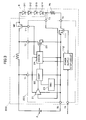
- FIG. 1 is a block diagram showing a conventional power supply circuit 1.
- the power supply circuit 1 includes a coil L, a boost control circuit 11, and a Schottky barrier diode D0 for rectification.
- a DC power supply 2 is connected to one end (a first end) of the coil L so that supply voltage Vcc is applied thereto.
- the boost control circuit 11 controls current flowing through the coil L.
- the Schottky barrier diode D0 rectifies current to a load 3 in accordance with voltage generated at the connection of the coil L and the boost control circuit 11, and supplies the current to the load 3.
- the boost control circuit 11 includes an error amplifier 21, a comparator 22, an oscillator circuit 23, a driver 24, a transistor 25, and a power supply stop circuit 26.
- the boost control circuit 11 is driven by the supply voltage Vcc supplied to a terminal T1 from the DC power supply 2.
- the error amplifier 21 is connected to a terminal T3.
- the terminal T3 is connected to the connection of the load 3 and one end of a detection resistor Rs.
- the other end of the detection resistor Rs is grounded through terminals T4 and T5.
- the error amplifier 21 amplifies voltage at the connection of the load 3 and the detection resistor Rs, and supplies the amplified voltage to the comparator 22.
- a detection signal from the error amplifier 21 and an oscillation signal from the oscillator circuit 23 are provided to the comparator 22.
- the oscillator circuit 23 generates a sawtooth or triangle wave oscillation signal.
- the comparator 22 compares the magnitudes of the detection signal provided from the error amplifier 21 and the sawtooth or triangle wave oscillation signal provided from the oscillator circuit 23. As a result, the comparator 22 generates a pulse signal whose pulse width increases as the detection signal level lowers and decreases as the detection signal level rises.
- the pulse signal generated in the comparator 22 is provided to the driver 24.
- the driver 24 switches on and off the transistor 25 in accordance with the pulse signal provided from the comparator 22.
- the transistor 25 has a drain thereof connected to the other end (a second end) of the coil L through a terminal T2 and a source thereof grounded.
- connection of the second end of the coil L and the terminal T2 is connected to the load 3 via the Schottky barrier diode D0.
- the Schottky barrier diode D0 is connected in the forward direction toward the load 3 between the connection of the second end of the coil L and the terminal T2 and the load 3.
- the voltage at the terminal T2 increased by the coil L is supplied to the load 3 via the Schottky barrier diode D0.
- the load 3 is composed of, for instance, light emitting diodes D11 through D14.
- the light emitting diodes D11 through D14 are connected in series and caused to emit light by the increased voltage.
- a lighting device that causes a light emitting diode to emit light by voltage increased by a power supply circuit has been disclosed in Japanese Laid-Open Patent Application No. 2002-258363.
- the increasing of voltage, the supplying of the increased voltage to the load 3, and the operation of the load 3 are stopped by maintaining the transistor 25 in OFF state.
- the DC power supply 2 and the load 3 are connected via the Schottky barrier diode D0, which is connected in the forward direction with respect to the coil L and the supply voltage Vcc. Therefore, when the transistor 25 is switched off, the supply voltage Vcc is applied to the load 3 through the Schottky barrier diode D0, so that a small current flows through the load 3.
- a more specific object of the present invention is to provide a power supply circuit and a power supply control method therein that can reduce power consumption.
- a power supply circuit including: a coil having first and second ends, the coil having supply voltage applied to the first end thereof; a first element connected between the second end of the coil and ground, the first element being a switching element; a second element configured to rectify current to be supplied to a load in accordance with voltage generated at a connection of the coil and the first element, and to supply the current to the load; a driver circuit configured to switch at least the first element; a third element connected in series to the load, the third element being a switching element; and a power supply stop circuit configured to switch off the first element so as to stop supplying power to the load and switch off the third element so as to stop supplying the current to the load in accordance with an external signal.
- a method of controlling supply of power in a power supply control circuit including a coil having first and second ends, the coil having supply voltage applied to the first end thereof; a first element connected between the second end of the coil and ground, the first element being a switching element; a second element configured to rectify current to be supplied to a load in accordance with voltage generated at a connection of the coil and the first element, and to supply the current to the load; and a driver circuit configured to switch at least the first element, wherein a third element is connected in series between the load and the ground, the third element being a switching element; and the third element is switched off when supplying the power to the load is stopped.
- a power supply circuit including a coil having first and second ends, the coil having supply voltage applied to the first end thereof, a first element connected between the second end of the coil and ground, the first element being a switching element; a second element rectifying current to be supplied to a load in accordance with voltage generated at the connection of the coil and the first element, and supplying the current to the load, and a driver circuit switching at least the first element, a third element, which is a switching element, is connected in series between the load and the ground.
- FIG. 2 is a block diagram showing a power supply circuit 100 according to a first embodiment of the present invention.
- the same elements as those of FIG. 1 are referred to by the same numerals, and a description thereof is omitted.
- the power supply circuit 100 of this embodiment is different from the conventional power supply circuit 1 (FIG. 1) in the configuration of a boost control circuit.
- the power supply circuit 100 includes a boost control circuit 101.
- the boost control circuit 101 which is formed of an IC (integrated circuit) chip, includes the error amplifier 21, the comparator 22, the oscillator circuit 23, the driver 24, the transistor 25, a transistor 111, and a power supply stop circuit 112.
- the transistor 25 forms a first switching element
- the Schottky barrier diode D0 for rectification forms a second switching or diode element
- the transistor 111 forms a third switching element.
- the transistor 111 is formed of, for instance, an n-channel MOS field effect transistor (MOSFET), and has a drain thereof connected to the terminal T4 and a source thereof connected to the terminal T5.
- a parasitic diode is connected to the transistor 111 in the forward direction from the terminal T5 to the terminal T4.
- a switching control signal is provided from the power supply stop circuit 112 to the gate of the transistor 111.
- the power supply stop circuit 112 is connected to a terminal T6.
- a stop instruction signal is provided to the terminal 6 from a host apparatus.
- the terminal T6 turns LOW (low level) based on the stop instruction signal provided from the host apparatus, the power supply stop circuit 112 enters a state to drive the load 3.
- the power supply stop circuit 112 switches a control signal provided to the driver 24 to LOW, and switches the gate of the transistor 111 to HIGH (high level).
- the driver 24 When the control signal from the power supply stop circuit 112 to the driver 24 turns LOW, the driver 24 enters an operative state, and provides a pulse signal in accordance with the output of the comparator 22 to the gate of the transistor 25.
- the transistor 25 is switched on and off in accordance with the pulse signal provided from the driver 24.
- the transistor 25 When the transistor 25 is switched on, current flows through the coil L. As a result of the current flowing through the coil L, electromagnetic energy is stored therein in accordance with the flowing current.
- the transistor is switched off, increased voltage is generated at the second end of the coil L in accordance with a back electromotive force. The increased voltage generated at the second end of the coil L is applied to the load 3 via the Schottky barrier diode D0.
- the power supply stop circuit 112 switches the control signal provided to the driver 24 to HIGH, and switches the gate of the transistor 111 to LOW.
- the driver 24 When the control signal provided from the power supply stop circuit 112 to the driver 24 turns HIGH, the driver 24 enters an inoperative state, and maintains the gate of the transistor 25 at LOW irrespective of the output of the comparator 22.
- the transistor 25 When the gate of the transistor 25 is held at LOW, the transistor 25 is maintained in OFF state. When the transistor 25 is maintained in OFF state, no change is caused in the current flowing through the coil L. Accordingly, the supply voltage from the power supply 2 is not increased, and is applied to the connection of the coil L and the Schottky barrier diode D0. Therefore, voltage obtained by subtracting the forward direction voltage Vf of the Schottky barrier diode D0 from the supply voltage Vcc (Vcc - Vf) is applied to the load 3.
- the transistor 111 can be reduced in size by being provided on the ground side of the load 3.
- the power supply stop circuit 112 stops the operation of the driver 24, thereby switching off the transistor 25.
- the power supply stop circuit 112 switches off the transistor 111 at the time of stopping supplying power.
- the transistor 111 is switched off, electric potential at the terminal T3 increases greatly compared with a normal operation period.
- the output of the comparator 22 is constantly kept LOW.
- the transistor 25 is constantly kept OFF by the driver 24. Accordingly, the transistor 25 can be switched off by normal operation without the power supply stop circuit 112 controlling the operation of the driver 24.
- current flowing through the terminal T3 is so small that current of such magnitude as to cause the diodes D11 through D14 to emit light is prevented from flowing through the diodes D11 through D14.
- FIG. 3 is a block diagram showing a power supply circuit 200 according to a second embodiment of the present invention.
- the same elements as those of FIG. 2 are referred to by the same numerals, and a description thereof is omitted.
- This embodiment is an application of the present invention to a power supply circuit of a synchronous rectification type.
- the power supply circuit 200 of this embodiment employs a p-channel MOSFET Q0 instead of the Schottky barrier diode D0 as the second switching or diode element.
- the power supply circuit 200 includes a boost control circuit 201.
- the boost control circuit 201 is formed of a single-chip IC.
- the driver 24 of the boost control circuit 201 controls the transistor 25, and also controls the transistor Q0 via a terminal T11. At this point, the transistor Q0 and the transistor 25 are switched on (off) alternately so that so-called synchronous rectification is performed.
- the terminal T11 is connected to the gate of the transistor Q0 forming the second switching or diode element.
- the transistor Q0 is switched on when the transistor 25 (the first switching element) is switched off, and is switched off when the transistor 25 is switched on.
- the transistor Q0 when the voltage at the second end of the coil L is increased, the transistor Q0 is switched on so that the increased voltage is applied to the load 3. On the other hand, when the voltage at the second end of the coil L is decreased, the transistor Q0 is switched off so as to prevent voltage drop at one end of the load 3.
- FIG. 4 is a block diagram showing a power supply circuit 300 according to a third embodiment of the present invention.
- the same elements as those of FIG. 2 are referred to by the same numerals, and a description thereof is omitted.
- the power supply circuit includes a transistor 311 serving as a third switching element connected in series between the diode D0 and the load 3.
- the transistor 311 is formed of a p-channel MOSFET transistor.
- the source, drain, gate, and back gate of the transistor 311 are connected to the cathode of the diode D0, the load 3, a power supply stop circuit 312 of a boost control circuit 301, and the gate of the transistor 311, respectively.
- the power supply stop circuit 312 provides a switching control signal to the transistor 311.
- the voltage level of the switching control signal at the time of the power supply stop circuit 312 switching off the transistor 311 (OFF potential V OFF ) is approximately equal to the supply voltage V DD supplied from the power supply 2.
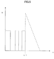
- FIG. 5 is a waveform chart according to the third embodiment of the present invention.
- the transistor 311 When the transistor 311 is switched off with the transistor 25 being in OFF state at Time t1 in order to cut off the supply of power to the load 3, the back electromotive force of the coil L causes the potential at the terminal T2 to be higher than the supply voltage V DD . At this point, the gate potential of the transistor 311 is approximately equal to the supply voltage V DD . Therefore, the transistor 311 is switched on, so that current flows from the coil L to the load 3.
- FIG. 6 is a block diagram showing a power supply circuit 400 according to a fourth embodiment of the present invention.
- the same elements as those of FIG. 4 are referred to by the same numerals, and a description thereof is omitted.
- the power supply circuit 400 is different from the power supply circuit 300 of the third embodiment in the configuration of a boost control circuit.
- the power supply circuit 400 includes a boost control circuit 401.
- a transistor 411 serving as a third switching element is contained in an IC chip forming the boost control circuit 401, and terminals T41 and T42 are provided.
- the terminal T41 is connected to the source of the transistor 411 inside the boost control circuit 401, and is connected to the cathode of the diode D0 outside the boost control circuit 401. Further, the terminal T42 is connected to the drain of the transistor 411 inside the boost control circuit 401, and is connected to the load 3 outside the boost control circuit 401.
- the number of externally attached components can be reduced. Accordingly, the power supply circuit 400 can be reduced in size and cost.
- FIG. 7 is a block diagram showing a power supply circuit 500 according to a fifth embodiment of the present invention.
- the same elements as those of FIG. 3 are referred to by the same numerals, and a description thereof is omitted.
- the power supply circuit 500 is different from the power supply circuit 200 of the second embodiment in the configuration of a boost control circuit.
- the power supply circuit 500 includes a boost control circuit 501.
- a transistor 511 serving as a second switching or diode element and a transistor 512 serving as a third switching element are contained in an IC chip forming the boost control circuit 501, and terminals T51 and T52 are provided.
- the terminal T51 is connected to the source of the transistor 511 inside the boost control circuit 501, and is connected to the connection of the second end of the coil L and the terminal T2 outside the boost control circuit 501.
- the source of the transistor 511 is connected to the source of the transistor 512.
- a switching control signal is provided from the driver 24 to the gate of the transistor 511.
- the transistor 511 is switched alternately with the transistor 25, which is the first switching element, by the switching control signal provided from the driver 24.
- the drain of the transistor 512 is connected to the terminal T52.
- the terminal T52 is connected to the load 3 outside the boost control circuit 501.
- the transistor 512 is switched by a switching signal provided from the power supply stop circuit 112.
- the transistor 512 is switched off at the time of stopping supplying power to the load 3, so that leakage current is prevented from flowing through the load 3.
- the number of externally attached components can be reduced. Accordingly, the power supply circuit 400 can be reduced in size and cost.
Landscapes
- Engineering & Computer Science (AREA)
- Power Engineering (AREA)
- Dc-Dc Converters (AREA)
- Electronic Switches (AREA)
- Direct Current Feeding And Distribution (AREA)
Abstract
Description
- The present invention relates generally to power supply circuits and power supply control methods therein, and more particularly to a power supply circuit and a power supply control method therein, the power supply circuit including a coil having supply voltage applied to one end thereof, a first switching element connected between the other end of the coil and ground, a second switching or diode element rectifying and supplying current to be supplied to a load in accordance with voltage generated at the connection of the coil and the first switching element, and a driver circuit switching at least the first switching element.
- FIG. 1 is a block diagram showing a conventional
power supply circuit 1. - Referring to FIG. 1, the
power supply circuit 1 includes a coil L, aboost control circuit 11, and a Schottky barrier diode D0 for rectification. ADC power supply 2 is connected to one end (a first end) of the coil L so that supply voltage Vcc is applied thereto. Theboost control circuit 11 controls current flowing through the coil L. The Schottky barrier diode D0 rectifies current to aload 3 in accordance with voltage generated at the connection of the coil L and theboost control circuit 11, and supplies the current to theload 3. - The
boost control circuit 11 includes anerror amplifier 21, acomparator 22, anoscillator circuit 23, adriver 24, atransistor 25, and a powersupply stop circuit 26. Theboost control circuit 11 is driven by the supply voltage Vcc supplied to a terminal T1 from theDC power supply 2. - The
error amplifier 21 is connected to a terminal T3. The terminal T3 is connected to the connection of theload 3 and one end of a detection resistor Rs. The other end of the detection resistor Rs is grounded through terminals T4 and T5. Theerror amplifier 21 amplifies voltage at the connection of theload 3 and the detection resistor Rs, and supplies the amplified voltage to thecomparator 22. - A detection signal from the
error amplifier 21 and an oscillation signal from theoscillator circuit 23 are provided to thecomparator 22. Theoscillator circuit 23 generates a sawtooth or triangle wave oscillation signal. Thecomparator 22 compares the magnitudes of the detection signal provided from theerror amplifier 21 and the sawtooth or triangle wave oscillation signal provided from theoscillator circuit 23. As a result, thecomparator 22 generates a pulse signal whose pulse width increases as the detection signal level lowers and decreases as the detection signal level rises. The pulse signal generated in thecomparator 22 is provided to thedriver 24. - The
driver 24 switches on and off thetransistor 25 in accordance with the pulse signal provided from thecomparator 22. Thetransistor 25 has a drain thereof connected to the other end (a second end) of the coil L through a terminal T2 and a source thereof grounded. - When the
transistor 25 is switched on by the pulse signal provided from thedriver 24, voltage at theterminal 2 is increased by the electromotive force of the coil L in accordance with the cycle of the pulse signal. - The connection of the second end of the coil L and the terminal T2 is connected to the
load 3 via the Schottky barrier diode D0. The Schottky barrier diode D0 is connected in the forward direction toward theload 3 between the connection of the second end of the coil L and the terminal T2 and theload 3. - The voltage at the terminal T2 increased by the coil L is supplied to the
load 3 via the Schottky barrier diode D0. - The
load 3 is composed of, for instance, light emitting diodes D11 through D14. The light emitting diodes D11 through D14 are connected in series and caused to emit light by the increased voltage. As related art, a lighting device that causes a light emitting diode to emit light by voltage increased by a power supply circuit has been disclosed in Japanese Laid-Open Patent Application No. 2002-258363. - However, according to the conventional
power supply circuit 1 shown in FIG. 1, the increasing of voltage, the supplying of the increased voltage to theload 3, and the operation of theload 3 are stopped by maintaining thetransistor 25 in OFF state. At this point, theDC power supply 2 and theload 3 are connected via the Schottky barrier diode D0, which is connected in the forward direction with respect to the coil L and the supply voltage Vcc. Therefore, when thetransistor 25 is switched off, the supply voltage Vcc is applied to theload 3 through the Schottky barrier diode D0, so that a small current flows through theload 3. - This increases power consumption. Further, when the
load 3 is a light emitting diode as in this case, there is a problem in that the light emitting diode emits light. - Accordingly, it is a general object of the present invention to provide a power supply circuit and a power supply control method therein in which the above-described disadvantage is eliminated.
- A more specific object of the present invention is to provide a power supply circuit and a power supply control method therein that can reduce power consumption.
- The above objects of the present invention are achieved by a power supply circuit including: a coil having first and second ends, the coil having supply voltage applied to the first end thereof; a first element connected between the second end of the coil and ground, the first element being a switching element; a second element configured to rectify current to be supplied to a load in accordance with voltage generated at a connection of the coil and the first element, and to supply the current to the load; a driver circuit configured to switch at least the first element; a third element connected in series to the load, the third element being a switching element; and a power supply stop circuit configured to switch off the first element so as to stop supplying power to the load and switch off the third element so as to stop supplying the current to the load in accordance with an external signal.
- The above objects of the present invention are also achieved by a method of controlling supply of power in a power supply control circuit including a coil having first and second ends, the coil having supply voltage applied to the first end thereof; a first element connected between the second end of the coil and ground, the first element being a switching element; a second element configured to rectify current to be supplied to a load in accordance with voltage generated at a connection of the coil and the first element, and to supply the current to the load; and a driver circuit configured to switch at least the first element, wherein a third element is connected in series between the load and the ground, the third element being a switching element; and the third element is switched off when supplying the power to the load is stopped.
- According to one embodiment of the present invention, in a power supply circuit including a coil having first and second ends, the coil having supply voltage applied to the first end thereof, a first element connected between the second end of the coil and ground, the first element being a switching element; a second element rectifying current to be supplied to a load in accordance with voltage generated at the connection of the coil and the first element, and supplying the current to the load, and a driver circuit switching at least the first element, a third element, which is a switching element, is connected in series between the load and the ground. When supplying power to the load is stopped, by switching off the third element, it is possible to prevent supply voltage from being supplied to the load through the coil and the second element for rectification in a state where the first element is switched off so that supplying increased voltage to the load is stopped. As a result, power consumption during the stoppage of the load can be reduced. Further, it is possible to prevent the load from being driven by a small current when the load is stopped.
- Other objects, features and advantages of the present invention will become more apparent from the following detailed description when read in conjunction with the accompanying drawings, in which:
- FIG. 1 is a block diagram showing a conventional power supply circuit;
- FIG. 2 is a block diagram showing a power supply circuit according to a first embodiment of the present invention;
- FIG. 3 is a block diagram showing a power supply circuit according to a second embodiment of the present invention;
- FIG. 4 is a block diagram showing a power supply circuit according to a third embodiment of the present invention;
- FIG. 5 is a waveform chart according to the third embodiment of the present invention;
- FIG. 6 is a block diagram showing a power supply circuit according to a fourth embodiment of the present invention; and
- FIG. 7 is a block diagram showing a power supply circuit according to a fifth embodiment of the present invention.
-
- A description is given below, with reference to the accompanying drawings, of embodiments of the present invention.
- FIG. 2 is a block diagram showing a
power supply circuit 100 according to a first embodiment of the present invention. In FIG. 2, the same elements as those of FIG. 1 are referred to by the same numerals, and a description thereof is omitted. - The
power supply circuit 100 of this embodiment is different from the conventional power supply circuit 1 (FIG. 1) in the configuration of a boost control circuit. - The
power supply circuit 100 includes aboost control circuit 101. Theboost control circuit 101, which is formed of an IC (integrated circuit) chip, includes theerror amplifier 21, thecomparator 22, theoscillator circuit 23, thedriver 24, thetransistor 25, atransistor 111, and a powersupply stop circuit 112. In this embodiment, thetransistor 25 forms a first switching element, the Schottky barrier diode D0 for rectification forms a second switching or diode element, and thetransistor 111 forms a third switching element. - The
transistor 111 is formed of, for instance, an n-channel MOS field effect transistor (MOSFET), and has a drain thereof connected to the terminal T4 and a source thereof connected to the terminal T5. A parasitic diode is connected to thetransistor 111 in the forward direction from the terminal T5 to the terminal T4. A switching control signal is provided from the powersupply stop circuit 112 to the gate of thetransistor 111. - The power
supply stop circuit 112 is connected to a terminal T6. A stop instruction signal is provided to the terminal 6 from a host apparatus. When the terminal T6 turns LOW (low level) based on the stop instruction signal provided from the host apparatus, the powersupply stop circuit 112 enters a state to drive theload 3. The powersupply stop circuit 112 switches a control signal provided to thedriver 24 to LOW, and switches the gate of thetransistor 111 to HIGH (high level). - When the control signal from the power
supply stop circuit 112 to thedriver 24 turns LOW, thedriver 24 enters an operative state, and provides a pulse signal in accordance with the output of thecomparator 22 to the gate of thetransistor 25. - The
transistor 25 is switched on and off in accordance with the pulse signal provided from thedriver 24. When thetransistor 25 is switched on, current flows through the coil L. As a result of the current flowing through the coil L, electromagnetic energy is stored therein in accordance with the flowing current. Next, when the transistor is switched off, increased voltage is generated at the second end of the coil L in accordance with a back electromotive force. The increased voltage generated at the second end of the coil L is applied to theload 3 via the Schottky barrier diode D0. - When the terminal T6 turns HIGH based on the stop instruction signal provided from the host apparatus, the power
supply stop circuit 112 switches the control signal provided to thedriver 24 to HIGH, and switches the gate of thetransistor 111 to LOW. - When the control signal provided from the power
supply stop circuit 112 to thedriver 24 turns HIGH, thedriver 24 enters an inoperative state, and maintains the gate of thetransistor 25 at LOW irrespective of the output of thecomparator 22. - When the gate of the
transistor 25 is held at LOW, thetransistor 25 is maintained in OFF state. When thetransistor 25 is maintained in OFF state, no change is caused in the current flowing through the coil L. Accordingly, the supply voltage from thepower supply 2 is not increased, and is applied to the connection of the coil L and the Schottky barrier diode D0. Therefore, voltage obtained by subtracting the forward direction voltage Vf of the Schottky barrier diode D0 from the supply voltage Vcc (Vcc - Vf) is applied to theload 3. - When the switching control signal provided from the power
supply stop circuit 112 to thetransistor 111 turns LOW, the gate of thetransistor 111 is switched to LOW, so that thetransistor 111 is switched off. When thetransistor 111 is switched off, the terminal T4 becomes open. When the terminal T4 becomes open, no current flows through theload 3 and the detection resistor Rs. - Thus, when the operation of increasing voltage (a voltage increase operation) is stopped, current is prevented from flowing through the
load 3, thus preventing unnecessary power consumption. Accordingly, power consumption can be reduced. - Further, the
transistor 111 can be reduced in size by being provided on the ground side of theload 3. - According to this embodiment, the power
supply stop circuit 112 stops the operation of thedriver 24, thereby switching off thetransistor 25. Alternatively, it is also possible to switch off thetransistor 25 by a feedback loop for controlling the current of theload 3 without the powersupply stop circuit 112 controlling the operation of thedriver 24. - In this case, first, the power
supply stop circuit 112 switches off thetransistor 111 at the time of stopping supplying power. When thetransistor 111 is switched off, electric potential at the terminal T3 increases greatly compared with a normal operation period. When the electric potential at the terminal T3 increases greatly, the output of thecomparator 22 is constantly kept LOW. When the output of thecomparator 22 is constantly kept LOW, thetransistor 25 is constantly kept OFF by thedriver 24. Accordingly, thetransistor 25 can be switched off by normal operation without the powersupply stop circuit 112 controlling the operation of thedriver 24. At this point, current flowing through the terminal T3 is so small that current of such magnitude as to cause the diodes D11 through D14 to emit light is prevented from flowing through the diodes D11 through D14. - FIG. 3 is a block diagram showing a
power supply circuit 200 according to a second embodiment of the present invention. In FIG. 3, the same elements as those of FIG. 2 are referred to by the same numerals, and a description thereof is omitted. - This embodiment is an application of the present invention to a power supply circuit of a synchronous rectification type.
- In contrast to the
power supply circuit 100 of the first embodiment (FIG. 2), thepower supply circuit 200 of this embodiment employs a p-channel MOSFET Q0 instead of the Schottky barrier diode D0 as the second switching or diode element. - The
power supply circuit 200 includes aboost control circuit 201. Theboost control circuit 201 is formed of a single-chip IC. Thedriver 24 of theboost control circuit 201 controls thetransistor 25, and also controls the transistor Q0 via a terminal T11. At this point, the transistor Q0 and thetransistor 25 are switched on (off) alternately so that so-called synchronous rectification is performed. - The terminal T11 is connected to the gate of the transistor Q0 forming the second switching or diode element. The transistor Q0 is switched on when the transistor 25 (the first switching element) is switched off, and is switched off when the
transistor 25 is switched on. - Accordingly, when the voltage at the second end of the coil L is increased, the transistor Q0 is switched on so that the increased voltage is applied to the
load 3. On the other hand, when the voltage at the second end of the coil L is decreased, the transistor Q0 is switched off so as to prevent voltage drop at one end of theload 3. - Thus, a so-called synchronous rectification operation, in which rectification is performed by synchronizing the transistor Q0, which is the second switching or diode element, with the
transistor 25, which is the first switching element, is performed. - FIG. 4 is a block diagram showing a
power supply circuit 300 according to a third embodiment of the present invention. In FIG. 4, the same elements as those of FIG. 2 are referred to by the same numerals, and a description thereof is omitted. - The power supply circuit includes a
transistor 311 serving as a third switching element connected in series between the diode D0 and theload 3. - The
transistor 311 is formed of a p-channel MOSFET transistor. The source, drain, gate, and back gate of thetransistor 311 are connected to the cathode of the diode D0, theload 3, a powersupply stop circuit 312 of aboost control circuit 301, and the gate of thetransistor 311, respectively. - The power
supply stop circuit 312 provides a switching control signal to thetransistor 311. The voltage level of the switching control signal at the time of the powersupply stop circuit 312 switching off the transistor 311 (OFF potential VOFF) is approximately equal to the supply voltage VDD supplied from thepower supply 2. - Next, a description is given of an operation according to this embodiment.
- FIG. 5 is a waveform chart according to the third embodiment of the present invention.
- When the
transistor 311 is switched off with thetransistor 25 being in OFF state at Time t1 in order to cut off the supply of power to theload 3, the back electromotive force of the coil L causes the potential at the terminal T2 to be higher than the supply voltage VDD. At this point, the gate potential of thetransistor 311 is approximately equal to the supply voltage VDD. Therefore, thetransistor 311 is switched on, so that current flows from the coil L to theload 3. - As a result, a significant increase in the drain potential of the
transistor 25 as indicated by broken lines in FIG. 5 can be prevented at the time of cutting off the supply of power. Accordingly, it is possible to prevent damage to thetransistor 25 due to an increase in the potential at the terminal T2 because of the back electromotive force of the coil L at the time of cutting off the supply of power. - FIG. 6 is a block diagram showing a
power supply circuit 400 according to a fourth embodiment of the present invention. In FIG. 6, the same elements as those of FIG. 4 are referred to by the same numerals, and a description thereof is omitted. - The
power supply circuit 400 according to this embodiment is different from thepower supply circuit 300 of the third embodiment in the configuration of a boost control circuit. Thepower supply circuit 400 includes aboost control circuit 401. In theboost control circuit 401, atransistor 411 serving as a third switching element is contained in an IC chip forming theboost control circuit 401, and terminals T41 and T42 are provided. - The terminal T41 is connected to the source of the
transistor 411 inside theboost control circuit 401, and is connected to the cathode of the diode D0 outside theboost control circuit 401. Further, the terminal T42 is connected to the drain of thetransistor 411 inside theboost control circuit 401, and is connected to theload 3 outside theboost control circuit 401. - According to this embodiment, the number of externally attached components can be reduced. Accordingly, the
power supply circuit 400 can be reduced in size and cost. - FIG. 7 is a block diagram showing a
power supply circuit 500 according to a fifth embodiment of the present invention. In FIG. 7, the same elements as those of FIG. 3 are referred to by the same numerals, and a description thereof is omitted. - The
power supply circuit 500 according to this embodiment is different from thepower supply circuit 200 of the second embodiment in the configuration of a boost control circuit. Thepower supply circuit 500 includes aboost control circuit 501. In theboost control circuit 501, atransistor 511 serving as a second switching or diode element and atransistor 512 serving as a third switching element are contained in an IC chip forming theboost control circuit 501, and terminals T51 and T52 are provided. - The terminal T51 is connected to the source of the
transistor 511 inside theboost control circuit 501, and is connected to the connection of the second end of the coil L and the terminal T2 outside theboost control circuit 501. The source of thetransistor 511 is connected to the source of thetransistor 512. A switching control signal is provided from thedriver 24 to the gate of thetransistor 511. Thetransistor 511 is switched alternately with thetransistor 25, which is the first switching element, by the switching control signal provided from thedriver 24. - The drain of the
transistor 512 is connected to the terminal T52. The terminal T52 is connected to theload 3 outside theboost control circuit 501. Thetransistor 512 is switched by a switching signal provided from the powersupply stop circuit 112. Thetransistor 512 is switched off at the time of stopping supplying power to theload 3, so that leakage current is prevented from flowing through theload 3. - According to this embodiment, the number of externally attached components can be reduced. Accordingly, the
power supply circuit 400 can be reduced in size and cost. - The present invention is not limited to the specifically disclosed embodiments, and variations and modifications may be made without departing from the scope of the present invention.
Claims (11)
- A power supply circuit (100, 200, 300, 400, 500) including a coil (L) having first and second ends, the coil having supply voltage applied to the first end thereof; a first element (25) connected between the second end of the coil (L) and ground, the first element (25) being a switching element; a second element (D0, Q0, 511) configured to rectify current to be supplied to a load (3) in accordance with voltage generated at a connection of the coil (L) and the first element (25), and to supply the current to the load (3); and a driver circuit (21, 22, 23, 24) configured to switch at least the first element (25), characterized by:a third element (111, 311, 411, 512) connected in series to the load (3), the third element (111, 311, 411, 512) being a switching element; anda power supply stop circuit (112, 312) configured to switch off the first element (25) so as to stop supplying power to the load (3) and switch off the third element (111, 311, 411, 512) so as to stop supplying the current to the load (3) in accordance with an external signal.
- The power supply circuit as claimed in claim 1, characterized in that the second element comprises a diode connected in a forward direction toward the load between the connection of the coil and the first element and the load.
- The power supply circuit as claimed in claim 1, characterized in that the second element is a switching element.
- The power supply circuit as claimed in claim 3, characterized in that the second element is driven in synchronization with the first element by the driver circuit so as to perform synchronous rectification.
- The power supply circuit as claimed in claim 1, characterized in that the third element is connected in series between the load and base potential.
- The power supply circuit as claimed in claim 1, characterized in that the third element is connected in series between the load and the second element.
- The power supply circuit as claimed in claim 1, characterized in that the third element comprises a MOS field effect transistor to which a parasitic diode is connected in a reverse direction.
- The power supply circuit as claimed in claim 1, characterized in that the third element is provided inside a semiconductor integrated circuit including at least the driver circuit.
- A method of controlling supply of power in a power supply control circuit (100, 200, 300, 400, 500) including a coil (L) having first and second ends, the coil (L) having supply voltage applied to the first end thereof; a first element (25) connected between the second end of the coil (L) and ground, the first element (25) being a switching element; a second element (D0, Q0, 511) configured to rectify current to be supplied to a load (3) in accordance with voltage generated at a connection of the coil (L) and the first element (25), and to supply the current to the load (3); and a driver circuit (21, 22, 23, 24) configured to switch at least the first element (25), characterized in that:a third element (111, 311, 411, 512) is connected in series between the load (3) and the ground, the third element (111, 311, 411, 512) being a switching element; andthe third element (111, 311, 411, 512) is switched off when supplying the power to the load (3) is stopped.
- The method as claimed in claim 9, characterized in that the second element comprises a diode connected in a forward direction toward the load between the connection of the coil and the first element and the load.
- The method as claimed in claim 9, characterized in that the second element is a switching element.
Applications Claiming Priority (2)
| Application Number | Priority Date | Filing Date | Title |
|---|---|---|---|
| JP2004024425 | 2004-01-30 | ||
| JP2004024425A JP4269959B2 (en) | 2004-01-30 | 2004-01-30 | Power supply circuit and power supply control method thereof |
Publications (2)
| Publication Number | Publication Date |
|---|---|
| EP1560321A2 true EP1560321A2 (en) | 2005-08-03 |
| EP1560321A3 EP1560321A3 (en) | 2006-02-22 |
Family
ID=34650861
Family Applications (1)
| Application Number | Title | Priority Date | Filing Date |
|---|---|---|---|
| EP04256963A Withdrawn EP1560321A3 (en) | 2004-01-30 | 2004-11-10 | Power supply circuit and power supply control method therein |
Country Status (4)
| Country | Link |
|---|---|
| US (1) | US7205727B2 (en) |
| EP (1) | EP1560321A3 (en) |
| JP (1) | JP4269959B2 (en) |
| CN (1) | CN100386937C (en) |
Cited By (2)
| Publication number | Priority date | Publication date | Assignee | Title |
|---|---|---|---|---|
| WO2007134871A1 (en) * | 2006-05-24 | 2007-11-29 | Austriamicrosystems Ag | Circuit arrangement and method for voltage conversion |
| DE102009000130A1 (en) * | 2009-01-09 | 2010-07-15 | Jb-Lighting Lichtanlagentechnik Gmbh | Lighting device for headlight, has switching arrangement that is controlled by control signal and disables current of controlled electrical power source for light emission via light source in switching condition |
Families Citing this family (13)
| Publication number | Priority date | Publication date | Assignee | Title |
|---|---|---|---|---|
| JP4655850B2 (en) * | 2005-09-28 | 2011-03-23 | ミツミ電機株式会社 | Power supply control circuit |
| JP5089193B2 (en) * | 2007-02-22 | 2012-12-05 | 株式会社小糸製作所 | Light emitting device |
| JP5228567B2 (en) * | 2008-03-26 | 2013-07-03 | ミツミ電機株式会社 | Boost DC-DC converter |
| JP4655111B2 (en) * | 2008-05-20 | 2011-03-23 | 日本テキサス・インスツルメンツ株式会社 | LED device and LED drive circuit |
| TWI400989B (en) * | 2008-05-30 | 2013-07-01 | Green Solution Technology Inc | Light emitting diode driving circuit and controller thereof |
| WO2011155295A1 (en) | 2010-06-10 | 2011-12-15 | Semiconductor Energy Laboratory Co., Ltd. | Dc/dc converter, power supply circuit, and semiconductor device |
| KR101730629B1 (en) | 2010-12-13 | 2017-04-27 | 페어차일드코리아반도체 주식회사 | Power converting apparatus and method of sensing output current thereof |
| JP6118316B2 (en) * | 2011-06-17 | 2017-04-19 | フィリップス ライティング ホールディング ビー ヴィ | DC-DC driver device with input and output filters for driving a load, in particular an LED unit |
| JP6460592B2 (en) | 2013-07-31 | 2019-01-30 | 株式会社半導体エネルギー研究所 | DC-DC converter and semiconductor device |
| JP2016139996A (en) * | 2015-01-28 | 2016-08-04 | 株式会社東芝 | Semiconductor device |
| JP6904798B2 (en) * | 2017-06-16 | 2021-07-21 | エイブリック株式会社 | Power supply |
| CN107171549A (en) * | 2017-06-21 | 2017-09-15 | 信利半导体有限公司 | A kind of DC voltage booster circuit |
| JP6983355B2 (en) * | 2018-07-18 | 2021-12-17 | エフィシエント パワー コンヴァーション コーポレーション | Current pulse generator with integrated bus boost circuit |
Family Cites Families (12)
| Publication number | Priority date | Publication date | Assignee | Title |
|---|---|---|---|---|
| US4682147A (en) * | 1985-06-28 | 1987-07-21 | Don Gilbert Industries, Inc. | Emergency sign |
| US5739639A (en) * | 1996-07-03 | 1998-04-14 | Nsi Enterprises, Inc. | Method and apparatus for operating LED array and charging battery for emergency LED operation including DC boost circuit allowing series connection of LED array and battery |
| JP3456121B2 (en) | 1997-09-09 | 2003-10-14 | 三菱電機株式会社 | Power control device for laser diode |
| FI106770B (en) * | 1999-01-22 | 2001-03-30 | Nokia Mobile Phones Ltd | Illuminating electronic device and lighting method |
| DE20023993U1 (en) | 2000-03-17 | 2008-09-25 | Tridonicatco Gmbh & Co. Kg | Control circuit for light emitting diodes |
| JP3284128B1 (en) * | 2000-05-12 | 2002-05-20 | ローム株式会社 | LED element driving circuit for illumination of display device in portable equipment |
| JP3529718B2 (en) | 2000-10-03 | 2004-05-24 | ローム株式会社 | Light emitting device of portable telephone and driving IC therefor |
| US6580222B2 (en) * | 2001-02-20 | 2003-06-17 | Durel Corporation | Inverter for driving EL lamp and light emitting diodes |
| JP4282910B2 (en) | 2001-03-05 | 2009-06-24 | 株式会社リコー | Lighting device for photography |
| US6791283B2 (en) * | 2001-09-07 | 2004-09-14 | Opalec | Dual mode regulated light-emitting diode module for flashlights |
| US6870328B2 (en) * | 2001-12-19 | 2005-03-22 | Toyoda Gosei Co., Ltd. | LED lamp apparatus for vehicles |
| JP2005006444A (en) | 2003-06-13 | 2005-01-06 | Japan Aviation Electronics Industry Ltd | Lighting lamp power supply |
-
2004
- 2004-01-30 JP JP2004024425A patent/JP4269959B2/en not_active Expired - Fee Related
- 2004-11-09 US US10/984,067 patent/US7205727B2/en not_active Expired - Lifetime
- 2004-11-10 EP EP04256963A patent/EP1560321A3/en not_active Withdrawn
- 2004-11-29 CN CNB2004100964200A patent/CN100386937C/en not_active Expired - Lifetime
Non-Patent Citations (1)
| Title |
|---|
| SHERMAN L.: "Logic Power Drives High-Intensity LEDs", ELECTRONIC DESIGN, PENTON MEDIA, vol. 43, no. 23, 23 October 1997 (1997-10-23), pages 142,144 |
Cited By (3)
| Publication number | Priority date | Publication date | Assignee | Title |
|---|---|---|---|---|
| WO2007134871A1 (en) * | 2006-05-24 | 2007-11-29 | Austriamicrosystems Ag | Circuit arrangement and method for voltage conversion |
| US8471490B2 (en) | 2006-05-24 | 2013-06-25 | Ams Ag | Circuit arrangement and method for voltage conversion |
| DE102009000130A1 (en) * | 2009-01-09 | 2010-07-15 | Jb-Lighting Lichtanlagentechnik Gmbh | Lighting device for headlight, has switching arrangement that is controlled by control signal and disables current of controlled electrical power source for light emission via light source in switching condition |
Also Published As
| Publication number | Publication date |
|---|---|
| CN100386937C (en) | 2008-05-07 |
| JP4269959B2 (en) | 2009-05-27 |
| JP2005217944A (en) | 2005-08-11 |
| EP1560321A3 (en) | 2006-02-22 |
| US7205727B2 (en) | 2007-04-17 |
| CN1649229A (en) | 2005-08-03 |
| US20050169022A1 (en) | 2005-08-04 |
Similar Documents
| Publication | Publication Date | Title |
|---|---|---|
| US7205727B2 (en) | Power supply circuit and power supply control method therein | |
| US7408796B2 (en) | Integrated synchronous rectifier package | |
| US6674268B2 (en) | Swithing regulator utilizing seperate integrated circuits for driving each switch | |
| US6469484B2 (en) | Power supply circuit and method thereof to detect demagnitization of the power supply | |
| US5774350A (en) | Integrated low dissipation power controller | |
| US8284533B2 (en) | Semiconductor device including a bootstrap diode, high side power drive circuit, low side power drive circuit, and control circuit for controlling a high side power device and low side power device | |
| US20100157629A1 (en) | Semiconductor laser apparatus | |
| CN100536309C (en) | Switching power supply device and switching method | |
| CN108123623B (en) | Rectifier and alternator using the same | |
| US20080203986A1 (en) | Boosting Switching regulator | |
| JP2022015506A (en) | Power supply control device | |
| CN112117904A (en) | Power converter, method and controller for controlling power converter | |
| US20200244180A1 (en) | Semiconductor device and method of operating the same | |
| US20230010170A1 (en) | Method of standby power supply | |
| CN113206604B (en) | Method and apparatus for generating control signals and charging DC power in a secondary synchronous rectifier | |
| WO2008115286A2 (en) | High-side current sense hysteretic led controller | |
| TWI871627B (en) | Rectifier circuit and power supply using the same | |
| US11705814B2 (en) | Switching control circuit and LLC converter | |
| US20040174721A1 (en) | Switching power supply unit | |
| JP3996147B2 (en) | Bootstrap capacitor charging circuit using a small charging current | |
| JP3702631B2 (en) | Inductive load drive | |
| JP2003198349A (en) | Output circuit device | |
| JP2006349417A (en) | Temperature abnormality detection device for solenoid drive transistor | |
| JP4007227B2 (en) | Inductive load controller | |
| JP7603484B2 (en) | Semiconductor drive circuit and power conversion device |
Legal Events
| Date | Code | Title | Description |
|---|---|---|---|
| PUAI | Public reference made under article 153(3) epc to a published international application that has entered the european phase |
Free format text: ORIGINAL CODE: 0009012 |
|
| AK | Designated contracting states |
Kind code of ref document: A2 Designated state(s): AT BE BG CH CY CZ DE DK EE ES FI FR GB GR HU IE IS IT LI LU MC NL PL PT RO SE SI SK TR |
|
| AX | Request for extension of the european patent |
Extension state: AL HR LT LV MK YU |
|
| PUAL | Search report despatched |
Free format text: ORIGINAL CODE: 0009013 |
|
| AK | Designated contracting states |
Kind code of ref document: A3 Designated state(s): AT BE BG CH CY CZ DE DK EE ES FI FR GB GR HU IE IS IT LI LU MC NL PL PT RO SE SI SK TR |
|
| AX | Request for extension of the european patent |
Extension state: AL HR LT LV MK YU |
|
| RIC1 | Information provided on ipc code assigned before grant |
Ipc: H05B 33/08 20060101ALI20060105BHEP Ipc: H02J 1/00 20060101ALI20060105BHEP Ipc: H02M 3/155 20060101AFI20050512BHEP |
|
| 17P | Request for examination filed |
Effective date: 20060419 |
|
| AKX | Designation fees paid |
Designated state(s): DE FR GB NL |
|
| 17Q | First examination report despatched |
Effective date: 20100122 |
|
| STAA | Information on the status of an ep patent application or granted ep patent |
Free format text: STATUS: THE APPLICATION IS DEEMED TO BE WITHDRAWN |
|
| 18D | Application deemed to be withdrawn |
Effective date: 20111201 |