EP1557842A2 - Associative memory apparatus for searching data in which Manhattan distance is minimum - Google Patents
Associative memory apparatus for searching data in which Manhattan distance is minimum Download PDFInfo
- Publication number
- EP1557842A2 EP1557842A2 EP04019069A EP04019069A EP1557842A2 EP 1557842 A2 EP1557842 A2 EP 1557842A2 EP 04019069 A EP04019069 A EP 04019069A EP 04019069 A EP04019069 A EP 04019069A EP 1557842 A2 EP1557842 A2 EP 1557842A2
- Authority
- EP
- European Patent Office
- Prior art keywords
- circuit
- data
- ref
- carrying
- manhattan distance
- Prior art date
- Legal status (The legal status is an assumption and is not a legal conclusion. Google has not performed a legal analysis and makes no representation as to the accuracy of the status listed.)
- Granted
Links
Images


Classifications
-
- G—PHYSICS
- G11—INFORMATION STORAGE
- G11C—STATIC STORES
- G11C15/00—Digital stores in which information comprising one or more characteristic parts is written into the store and in which information is read-out by searching for one or more of these characteristic parts, i.e. associative or content-addressed stores
-
- G—PHYSICS
- G11—INFORMATION STORAGE
- G11C—STATIC STORES
- G11C7/00—Arrangements for writing information into, or reading information out from, a digital store
- G11C7/10—Input/output [I/O] data interface arrangements, e.g. I/O data control circuits, I/O data buffers
-
- G—PHYSICS
- G11—INFORMATION STORAGE
- G11C—STATIC STORES
- G11C8/00—Arrangements for selecting an address in a digital store
- G11C8/10—Decoders
Definitions
- the present invention relates to an associative memory apparatus which is used for an apparatus for information processing such as color or gray scale image compression and image recognition, and which has a function of searching for data in which the Manhattan distance is a minimum by fully-parallel processing.
- the associative memory apparatus is one of the typical memories having a function of searching for data most similar (closest) to input information data (search data) from among a plurality of reference data registered in advance. Then, due to the excellent searching function, the associative memory apparatus is expected, when the associative memory apparatus is used for an application requiring a pattern matching function such as image compression and image recognition described above, to be able to greatly improve the performance of the pattern matching.
- the distance means a degree of inconsistency when search data and reference data are compared with one another, and it has been known that there are mainly the Hamming distance and the Manhattan distance.
- the Hamming distance between the ith reference data and the search data is expressed by:
- the Manhattan distance follows:
- the Hamming distance D Hamm is mainly used for recognizing data sequences, sound, characters, and the like, and the Manhattan distance D Manh is used for color or gray scale image compression/image recognition.
- a distance calculating circuit for searching for the a Hamming distance has been realized (refer to Document 1).
- a function of searching for the Manhattan distance needed for color or gray scale image compression/image recognition, or the like is realized at the memory region of the associative memory.
- An object of the present invention is to provide an associative memory apparatus which can realize a search for the Manhattan distance needed for color or gray scale image compression/image recognition at high speed and with a small area circuit by fully-parallel processing, and which is for searching for data in which the Manhattan distance is a minimum.
- an associative memory apparatus for searching reference data REF most similar to search data SW which is input with the same unit structure, from among W ⁇ R (W and R are arbitrary natural numbers) of reference data REF which are registered in advance in a memory region (100) and which are respectively made to be units in k-bit (k > 1) units, on the basis of an index of a Manhattan distance, the apparatus characterized by comprising:
- a reduction in a circuit scale and accelerating of calculating processing can be realized because all of the calculations of the absolute value of difference in the calculation of a Manhattan distance are realized by addition processing on the basis of a complement 2's, and a circuit configuration is scaled down due to it being determined whether an output signal is inverted by a carrying signal of the least significant bit, or 1 is added to the sum total of the outputs, by using dual signals (non-inversion signal and inversion signal) of a bit line of the search data existing at a unit storage circuit.
- a search of a minimum Manhattan distance can be realized with a chip configuration at a low electric power consumption and with a small area.
- a Manhattan distance calculating circuit needed for color and gray scale image compression/image recognition, or the like is developed, and a minimum Manhattan distance searching associative memory apparatus at a low electric power consumption and with a small area is realized.
- the circuit configuration can make a highly efficient fully-parallel associative memory apparatus be a chip by using a conventional CMOS technology with respect to a pattern matching application (for example, a network router, code book base data compression, and object recognition).
- FIG. 1 is a block diagram illustrating an architecture of a fully-parallel type associative memory apparatus using a Manhattan distance calculating circuit according to the present invention (refer to Document 1 or 4).
- a memory core portion is configured of a memory region (the left part) 100, a winner line-up amplification circuit (hereinafter, winner line-up amplifier [WLA] circuit) 200, and a total winner take all circuit (hereinafter, winner take-all [WTA] circuit) 300, and has a column decoder and R/W circuit (K ⁇ W Columns) 110, a row decoder (R Rows) 120, and a search data storage circuit (search data (K bits ⁇ W)) 130.
- WLA winner line-up amplifier
- WTA total winner take all circuit
- the memory region 100 is configured of W ⁇ R of unit storage circuits (unit storage: US) formed from SRAM cells for storing reference data in units (k bits), W ⁇ R of unit comparison circuits (unit comparison: UC) for calculating an absolute value of a difference between the reference data and the search data, i.e., a Manhattan distance, for each unit, and R of word weight comparison circuits (word comparison: WC) for converting the calculated distance into an analog voltage (or electric current).
- unit storage circuits unit storage: US
- UC unit comparison circuits
- word comparison: WC word comparison circuits
- a signal C (comparison signal) generated at the word weight comparison circuit WC enters the WLA circuit 200, and the WLA circuit 200 controls the signal C with the balance of the circuit itself, and amplifies the differences of the voltages between the respective rows to the maximums at the first stage.
- the WLA circuit 200 and the WTA circuit 300 have the feature that a ratio of an increase in areas with respect to the number of rows R becomes a linear O(R) with respect to the number of rows R.
- the WTA circuit 300 has a function of further amplifying the differences between voltage outputs LA of the respective rows amplified by the WLA circuit 200. With respect to the output M of the WTA circuit 300, a winner row is "1" digital signal, and the other loser rows are "0" digital signals.
- the WLA circuit 200 accelerates feedback by using a voltage follower circuit built in the WLA circuit 200 at the time of returning a feedback signal F to the word weight comparison circuit WC.
- the Manhattan distance calculating circuit used for the associative memory apparatus of the present invention is a circuit in which W of units corresponding to k bits (k > 1) that data to be dealt with are encoded are arranged as shown in FIG. 1. Given that the search data which will be an input of the associative memory apparatus and the reference data (i row) stored in the associative memory apparatus are respectively SW and REF i , a Manhattan distance between SW and REF i is expressed as the following formula.
- a Manhattan distance is used for image data processing by which comparison between the k-bit W of data such as a color image, a gray scale image, and the like is required.
- ) which generates absolute values of the differences between two k-bit data of W of the respective units.
- FIG. 2 is a block diagram (W units) illustrating a configuration, which is assembled in the associative memory apparatus, of the Manhattan distance calculating circuit with respect to the row i.
- US i1 to US iw are respectively unit storage circuits which fetch search data units in accordance with k-bit binary code data of non-inversion signals SW and inversion signals ⁇ SW ( ⁇ denotes inversion: hereinafter referred to as it), and which store the search data units along with the reference data unit stored in advance in bit units
- UC i1 to UC iw are respectively unit comparison circuits having a k-bit subtracter 11 and an absolute value calculating circuit 12, the unit comparison circuits receiving the search data SW and the reference data REF from the unit storage circuits US i1 to US iw , and calculating an absolute value of the difference between the both.
- FIG. 3 shows an example of a circuit, that one group shown in FIG. 2 (jth group in FIG. 3) is sampled out, at which a calculated result of the Manhattan distance is converted into an electric current value in consideration of the weight of each bit at the word weight comparison circuit WC i .
- weighting is carried out by adjusting output values OUT 1 , OUT 2 , ⁇ , OUT k of the respective bits so as to be 2 k-1 times electric current value of the OUT 1 which is the least significant bit, in accordance with the positions of the respective bits.
- weightings for the respective bits are carried out by controlling an value of electric current made to flow in a transistor connected to a match line in such a manner that a gate width W k of a transistor connected to the output OUT k of each bit is multiplied by an integer (2 k-1 ⁇ W 0 ) (W 0 denotes a transistor width serving as a reference).
- Electric current corresponding to the absolute value of the differences outputted from all of the unit comparison circuits UC i1 to UC iw is made to flow in the match line, and in accordance therewith, electric current corresponding to a Manhattan distance between the search data SW i and the reference data REF ij of each group is made to flow, so that an electric current value i corresponding to a Manhattan distance D manh between the total search data SW and the reference data REF can be obtained.
- the electric current value i is converted into a voltage value and transmitted to the WLA circuit 200 and the WTA circuit 300, a signal at a row at which a Manhattan distance is made to be a minimum (called a winner column) is amplified, and "1" is output from the winner row at which the distance is the minimum.
- the k-bit subtracter 11 and the absolute value calculating circuit 12 shown in FIG. 2 can be configured by using an adder, a selector, and an inverter which have been conventionally known.
- the entire configuration of the unit comparison circuit UC using adders, a selector, and an inverter is as that shown in FIG. 4B, and the respective k-bit circuit configurations are as shown those in FIG. 4C.
- a selector SEL requires about six transistors as shown in FIG. 5A
- a half adder HA requires about twelve transistors as shown in FIG. 5B
- a full adder FA requires about thirty transistors as shown in FIG.
- this absolute-value-of-difference calculating circuit is built into the fully-parallel type associative memory as an unit comparison circuit UC, and all of the outputs of W of the absolute-value-of-difference calculating circuit are inputted to the word weight comparison circuit WC and processed thereat, whereby the calculation of a Manhattan distance between the search data and the reference data is realized.
- the absolute-value-of-difference calculating circuit of the present invention is basically formed from two of the addition circuit and the bit inversion circuit.
- FIG. 6A is a diagram showing a method for calculating the absolute value of difference in the present invention
- FIG. 6B is a diagram showing a situation of the addition used for the calculation of the above-described absolute value of difference.
- a subtraction can be processed due to an addition by using a complement of 2. As shown in FIG.
- the SRAM cell of the unit storage circuit US is operated by dual signals (non-inversion signal SW and inversion signal ⁇ SW) of the bit line. Therefore, in the present invention, on the basis of the calculating method of FIG. 6A and Table 1, the circuit configuration is scaled down by determining whether the output signal is inverted by the carrying signal of the most significant bit, or 1 is added to the sum total of the outputs, by using the dual signals (non-inversion signal SW and inversion signal ⁇ SW) of the bit line which exist at the SRAM cell of the unit storage circuit US.
- FIG. 7 is a circuit diagram illustrating a configuration of a Manhattan distance calculating circuit of one group according to the present invention based on the above-described outline.
- the unit storage circuit US ij stores respective bit data REF 1 , REF 2 , ⁇ , REF k of the k-bit reference data of one unit into the SRAM cells S 1 , S 2 , ⁇ , S k .
- the respective cell output data are transmitted to the unit comparison circuit UC ij .
- the respective cell output data REF 1 , REF 2 , ⁇ , REF k are transmitted to XOR circuits A 1 , A 2 , ⁇ , A k which operate an exclusive OR, and are outputted so as to be inverted/non-inverted in accordance with bit data corresponding to the respective bit data SW i,j1 , SW i,j2 , ⁇ , SW i,jk (non-inversion signal and inversion signal) of the k-bit search data. Accordingly, subtraction between the bits of the search data and the reference data is realized by addition processing.
- the calculating circuit at each bit is configured of portions of XOR circuits B 2 , ⁇ , B k , carry generation circuits D 1 , D 2 , ⁇ , D k , and XOR circuits E 1 , E 2 , ⁇ , E k .
- the XOR circuits B 2 , ⁇ , B k carry out addition processing due to the exclusive OR of the bit output to which the unit storage circuit US ij corresponds and carrying data from less significant bits C 1 , C 2 , ⁇ , C k-1 .
- the XOR circuits E 1 , E 2 , ⁇ , E k are for inverting the addition processed results of the respective bits when the carrying data of the most significant bit is 0. With respect to only the least significant bit (LSB), because there is no carrying from the lower digit, the XOR circuit B for addition output is not required.
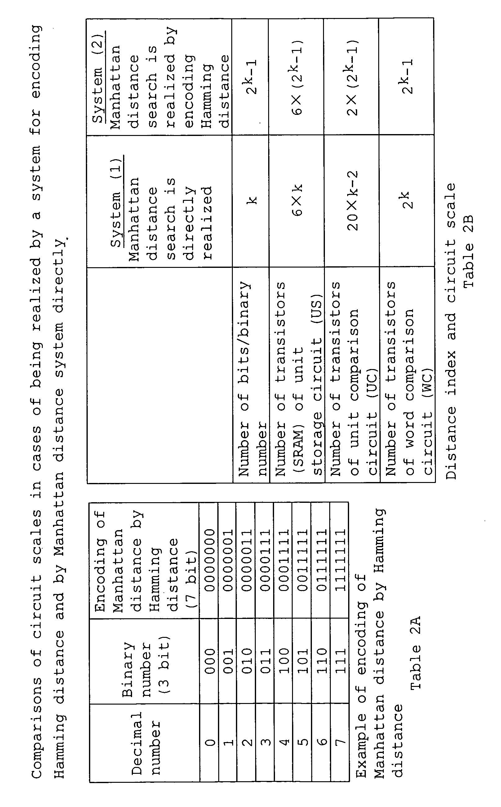
- Table 2 shows the comparison of the circuit scales in a case of realizing a Manhattan distance by a Hamming distance system (refer to Document 2) and in a case of realizing a Manhattan distance directly by the present invention.
- Table 2A shows an example of encoding of a Manhattan distance by a Hamming distance
- Table 2B shows the relationships between distance indices and circuit scales.
- Table 2B there is shown the relationship between the number of transistors and the number of bits k which are respectively required in the cases by a method (system 1) for realizing the Manhattan distance search directly by the circuit and a method (system 2) for realizing the Manhattan distance search by encoding a Hamming distance.
- mapping (encoding) is carried out with respect to the Manhattan distance search on the Hamming distance associative memory by solving Formula (6) with respect to k, it is possible make an area of the associative memory core small without increasing a minimum distance searching time up to a k ⁇ 3 bit binary number. However, in the case of k > 3 bits, a circuit area can be greatly reduced by directly realizing the Manhattan distance calculating circuit in the associative memory.
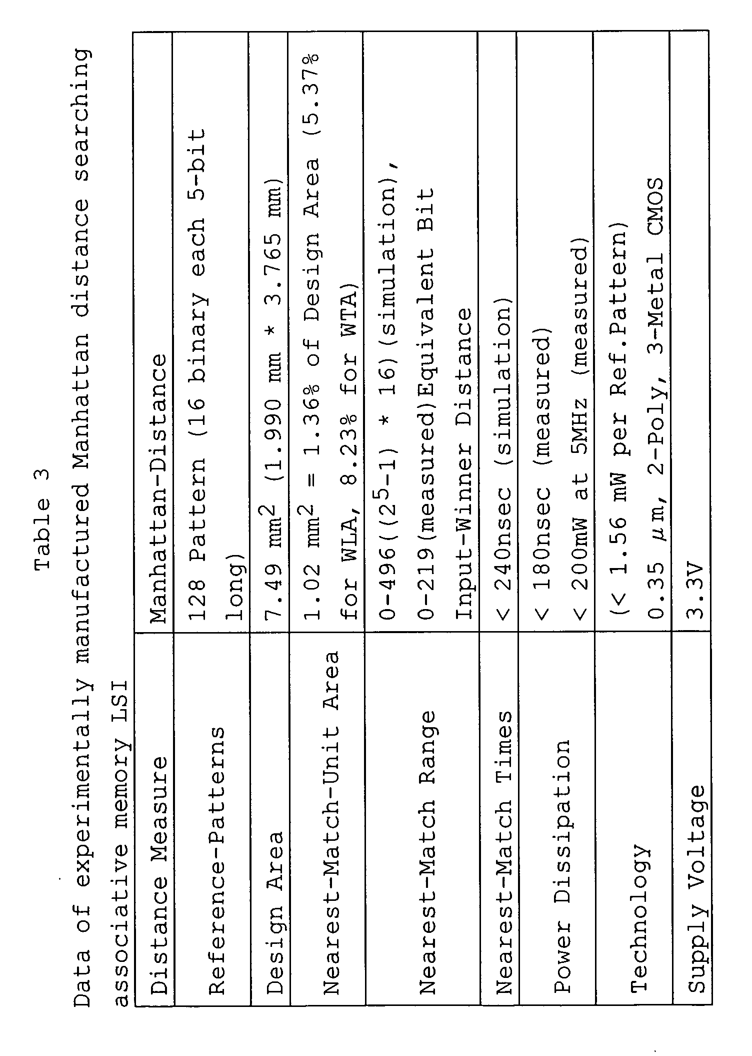
- 5-bit minimum Manhattan distance searching associative memory was designed by using a three-layered wiring 0.35 ⁇ m CMOS technology, an experimental manufacture of chip was carried out, and the performance thereof was evaluated.
- all of the circuits were realized so as to have an area of 7.49 mm 2 (1.990 mm ⁇ 3.765 mm), and among the circuits, winner search circuits (WLA circuit and WTA circuit) could be realized by only 13.6 % (1.02 mm 2 ) of the entire body.
- a microphotography of the associative memory for searching the minimum Manhattan distance which was experimentally manufactured is shown in FIG. 9.
- the abscissa stands for the distance (winner-input distance (bit)) between the search data (input) and the closest reference data (winner), and the ordinate stands for the time for searching the reference data (winner-search time (ns).
- the winner-loser distance in the graph stands for winner-search time in the cases of varying a distance between the reference data (loser) other than the closest reference data and the winner to 1 bit, 2 bits, 5 bits, and 10 bits. This simulation was executed supposing that one of the 128 reference data is a winner, and the other 127 reference data are losers with the same contents.
- the distances between the winner and the losers are set to the cases of 1 bit, 2 bits, 5 bits, and 10 bits which are difficult to search for.
- the searching time was 240 nsec or less with respect to the maximum distance 496 (5-bit ⁇ 16 units).
- the measured results of the chip which was experimentally manufactured are shown in FIG. 11. From the measured results, it can be understood that the winner-input distance (distance between the reference data and the search data) could be measured up to 219 at a maximum. Further, the winner searching time was 180 nsec or less. In consideration of the fact that, in most cases, a distance difference of the winner-input distances is 50 bits or less in the actual application (for example, image compression due to the vector quantization using a code book), it is possible to search at a high-speed not more than 180 nsec. The electric power consumption was 200 mW at 5 MHz at maximum, and about 1.56 mW at 5 MHz per one reference pattern, which is an extremely low electric power consumption. A list of the performances of the minimum Manhattan distance searching associative memory which was experimentally manufactured is shown in Table 3.
- the logic of the circuit shown in FIG. 7 is one example; the logic circuit may be inverted to positive logic or negative logic. For example, even if the N-MOS of the memory region is changed to P-MOS, or the P-MOS of the match line is changed to N-MOS, there is no change in the operation and effects thereof.
- the associative memory apparatus can be used for general compression and recognition processing techniques such as an artificial intelligence system, a data bank system, an Internet router, a mobile terminal (for example, a mobile video telephone), code book base data compression, and object recognition, etc.
- general compression and recognition processing techniques such as an artificial intelligence system, a data bank system, an Internet router, a mobile terminal (for example, a mobile video telephone), code book base data compression, and object recognition, etc.
Landscapes
- Engineering & Computer Science (AREA)
- Microelectronics & Electronic Packaging (AREA)
- Compression, Expansion, Code Conversion, And Decoders (AREA)
- Image Analysis (AREA)
Abstract
Description




Claims (4)
- An associative memory apparatus for searching reference data REF most similar to search data SW which is input with the same unit structure, from among W × R (W and R are arbitrary natural numbers) of reference data REF which are registered in advance in a memory region (100) and which are respectively made to be units in k-bit (k > 1) units, on the basis of an index of a Manhattan distance, the apparatus characterized by comprising:a distance calculating circuit (US, UC, WC) which is formed at the memory region (100), and which calculates an absolute value of difference |SW-REF| in parallel with the W × R of reference data REF with respect to the search data SW, and outputs a degree D of a inconsistency between both data of the calculated results as a "Manhattan distance"; anda searching circuit (200, 300) which searches reference data in which the calculated result of the Manhattan distance is made to be a minimum distance, characterized in thatthe distance calculating circuit (US, UC, WC) comprises W columns x R rows of unit storage circuits (US) to store the reference data in units, W columns x R rows of unit comparison circuits (UC) which calculate a Manhattan distance between the reference data and the search data for each unit, and R rows of word weight comparison circuits (WC) which generate an electric current signal or a voltage signal corresponding to a Manhattan distance calculated at the W columns of unit comparison circuits for each row, andthe unit comparison circuit (UC) compares magnitudes of the reference data REF and the search data SW, and when the compared result thereof is SW > REF, (SW+ (∼REF))+1 (∼ denotes inversion (a complement of 1): hereinafter referred to as it) is calculated, and when the compared result thereof is SW ≤ REF, ∼ (SW+ (∼REF)) is calculated.
- An associative memory apparatus according to claim 1, characterized in that
the unit comparison circuit (UC) comprises an addition circuit (A1, A2, ··· ,Ak, B2, ··· ,Bk) which calculates SW+(∼REF) by expressing subtraction processing used for the calculation of the absolute value of difference by addition processing, a carrying determining circuit (D1, D2, ··· , Dk) which determines presence/absence of a carrying of an MSB (a most significant bit) with respect to the calculated result of the addition circuit, and an output processing circuit (E1, E2, ··· , Ek) which outputs the calculated result of the addition circuit so as to be inverted when the carrying is "absent", and which adds 1 to the calculated result of the addition circuit and outputs it when the carrying is "present". - An associative memory apparatus according to claim 2, characterized in that
the addition circuit (A1, A2, ··· ,Ak, B2, ··· ,Bk) comprises a first arithmetic circuit (A1, A2, ··· ,Ak) which fetches respective bits of the search data by dual signals of a non-inversion signal and an inversion signal and operates an exclusive OR of those and bit outputs of the reference data, and a second arithmetic circuit (B2, ··· ,Bk) which operates an exclusive OR of output data of the first arithmetic circuit and carrying data from a less significant bit,
the carrying determining circuit (D1, D2, ··· , Dk) comprises a selection circuit (D1, D2, ... , Dk) which generates carrying data by selecting one of the bit data of the search data and the carrying data from the less significant bit on the basis of the output data of the first arithmetic circuit (A1, A2, ··· ,Ak), and
the output processing circuit (E1, E2, ··· , Ek) comprises an inversion circuit (E1, E2, ··· , Ek) which inverts respective bit outputs of the second arithmetic circuit (B2, ··· ,Bk) when it is determined that there is no carrying of the most significant bit at the carrying determining circuit (D1, D2, ··· , Dk), and an addition circuit which adds 1 to a sum total of the respective bit outputs of the second arithmetic circuit (B2, ··· ,Bk) when it is determined that there is carrying of the most significant bit at the carrying determining circuit (D1, D2, ··· , Dk). - An associative memory apparatus according to claim 3, characterized in that
the output processing circuit (E1, E2, ··· , Ek) directly outputs an output of the first arithmetic circuit with respect to a least significant bit.
Applications Claiming Priority (2)
| Application Number | Priority Date | Filing Date | Title |
|---|---|---|---|
| JP2004017429A JP2005209317A (en) | 2004-01-26 | 2004-01-26 | Minimum Manhattan distance search associative memory device |
| JP2004017429 | 2004-01-26 |
Publications (3)
| Publication Number | Publication Date |
|---|---|
| EP1557842A2 true EP1557842A2 (en) | 2005-07-27 |
| EP1557842A3 EP1557842A3 (en) | 2006-04-12 |
| EP1557842B1 EP1557842B1 (en) | 2008-10-15 |
Family
ID=34631980
Family Applications (1)
| Application Number | Title | Priority Date | Filing Date |
|---|---|---|---|
| EP04019069A Expired - Lifetime EP1557842B1 (en) | 2004-01-26 | 2004-08-11 | Associative memory apparatus for searching data in which Manhattan distance is minimum |
Country Status (6)
| Country | Link |
|---|---|
| US (1) | US7113416B2 (en) |
| EP (1) | EP1557842B1 (en) |
| JP (1) | JP2005209317A (en) |
| KR (1) | KR100549895B1 (en) |
| DE (1) | DE602004017115D1 (en) |
| TW (1) | TWI254258B (en) |
Families Citing this family (12)
| Publication number | Priority date | Publication date | Assignee | Title |
|---|---|---|---|---|
| JP2004013504A (en) * | 2002-06-06 | 2004-01-15 | Univ Hiroshima | Pattern recognition system, associative memory device used in this system, and pattern recognition processing method |
| JP4208958B2 (en) | 2007-02-27 | 2009-01-14 | 国立大学法人広島大学 | Amplifier circuit and associative memory |
| JP2009110211A (en) * | 2007-10-29 | 2009-05-21 | Sony Corp | Information encoding apparatus and method, information search apparatus and method, information search system and method, and program |
| JP4427574B2 (en) | 2007-11-30 | 2010-03-10 | 国立大学法人広島大学 | Associative memory and search system using the same |
| US8339824B2 (en) * | 2008-07-02 | 2012-12-25 | Cooke Laurence H | Nearest neighbor serial content addressable memory |
| US9129042B2 (en) * | 2008-07-02 | 2015-09-08 | Laurence H. Cooke | Nearest neighbor serial content addressable memory |
| WO2010013295A1 (en) | 2008-07-31 | 2010-02-04 | 国立大学法人広島大学 | Offset elimination circuit, associative memory equipped with the same, and offset voltage elimination method |
| US8022854B2 (en) | 2009-08-31 | 2011-09-20 | Semtech Corporation | Thermometer code transcoding and encoding methods and systems |
| JP5224601B2 (en) | 2009-10-01 | 2013-07-03 | 国立大学法人広島大学 | Associative memory |
| JP5800422B2 (en) * | 2011-11-07 | 2015-10-28 | 国立大学法人広島大学 | Associative memory |
| CN112687306B (en) * | 2020-12-31 | 2023-10-20 | 中国科学技术大学 | Distance calculation device and method based on NOR Flash |
| JP2024034521A (en) | 2022-08-31 | 2024-03-13 | キオクシア株式会社 | Information processing equipment and memory system |
Family Cites Families (2)
| Publication number | Priority date | Publication date | Assignee | Title |
|---|---|---|---|---|
| EP0859366A1 (en) * | 1997-02-12 | 1998-08-19 | STMicroelectronics S.r.l. | Associative memory device with optimized occupation, particularly for the recognition of words |
| JP2004013504A (en) * | 2002-06-06 | 2004-01-15 | Univ Hiroshima | Pattern recognition system, associative memory device used in this system, and pattern recognition processing method |
-
2004
- 2004-01-26 JP JP2004017429A patent/JP2005209317A/en active Pending
- 2004-08-11 DE DE602004017115T patent/DE602004017115D1/en not_active Expired - Lifetime
- 2004-08-11 US US10/915,430 patent/US7113416B2/en not_active Expired - Fee Related
- 2004-08-11 EP EP04019069A patent/EP1557842B1/en not_active Expired - Lifetime
- 2004-08-13 TW TW093124390A patent/TWI254258B/en not_active IP Right Cessation
- 2004-08-18 KR KR1020040064923A patent/KR100549895B1/en not_active Expired - Fee Related
Also Published As
| Publication number | Publication date |
|---|---|
| EP1557842B1 (en) | 2008-10-15 |
| TW200527323A (en) | 2005-08-16 |
| JP2005209317A (en) | 2005-08-04 |
| EP1557842A3 (en) | 2006-04-12 |
| US20050162878A1 (en) | 2005-07-28 |
| KR20050077003A (en) | 2005-07-29 |
| TWI254258B (en) | 2006-05-01 |
| DE602004017115D1 (en) | 2008-11-27 |
| US7113416B2 (en) | 2006-09-26 |
| KR100549895B1 (en) | 2006-02-06 |
Similar Documents
| Publication | Publication Date | Title |
|---|---|---|
| US7203382B2 (en) | Pattern matching and pattern recognition system, associative memory apparatus, and pattern matching and pattern recognition processing method | |
| US7113416B2 (en) | Associative memory apparatus for searching data in which manhattan distance is minimum | |
| JP7070653B2 (en) | Learning devices, speech recognition ranking estimators, their methods, and programs | |
| WO2022046199A1 (en) | Multi-token embedding and classifier for masked language models | |
| Jarollahi et al. | A low-power content-addressable memory based on clustered-sparse networks | |
| Macha et al. | Fixed-point quantization aware training for on-device keyword-spotting | |
| US6693815B2 (en) | Semiconductor associative memory | |
| US12451136B2 (en) | Audio caption generation method, audio caption generation apparatus, and program | |
| JP3731046B2 (en) | Semiconductor associative memory | |
| Graham | Low-precision batch-normalized activations | |
| US10747775B2 (en) | Data conversion device, search system, and method | |
| JP6820764B2 (en) | Acoustic model learning device and acoustic model learning program | |
| CN114239818A (en) | Memory computing architecture neural network accelerator based on TCAM and LUT | |
| JP4892720B2 (en) | Minimum Euclidean distance search associative memory device | |
| JP4208958B2 (en) | Amplifier circuit and associative memory | |
| US20230259330A1 (en) | Pipelines for power and area savings and for higher parallelism | |
| Kang et al. | ToEx: Accelerating generation stage of transformer-based language models via token-adaptive early exit | |
| JP4543307B2 (en) | Memory device and motion vector detection device | |
| Lin et al. | Accept: Adaptive codebook for composite and efficient prompt tuning | |
| Franti et al. | Fast implementation of the optimal PNN method | |
| Afifi et al. | STAR: A mixed analog stochastic in-DRAM convolutional neural network accelerator | |
| US7277909B2 (en) | High speed adder | |
| Wang et al. | Realization of bidirectional associative memory using a pseudo-parallel searching approach | |
| KR102845790B1 (en) | Computing in memory device sharing charges of bit lines to generate reference voltage and its operating method thereof | |
| Adkins et al. | Associative computation circuits for real-time processing of satellite communications and image pattern classification |
Legal Events
| Date | Code | Title | Description |
|---|---|---|---|
| PUAI | Public reference made under article 153(3) epc to a published international application that has entered the european phase |
Free format text: ORIGINAL CODE: 0009012 |
|
| 17P | Request for examination filed |
Effective date: 20040811 |
|
| AK | Designated contracting states |
Kind code of ref document: A2 Designated state(s): AT BE BG CH CY CZ DE DK EE ES FI FR GB GR HU IE IT LI LU MC NL PL PT RO SE SI SK TR |
|
| AX | Request for extension of the european patent |
Extension state: AL HR LT LV MK |
|
| PUAL | Search report despatched |
Free format text: ORIGINAL CODE: 0009013 |
|
| AK | Designated contracting states |
Kind code of ref document: A3 Designated state(s): AT BE BG CH CY CZ DE DK EE ES FI FR GB GR HU IE IT LI LU MC NL PL PT RO SE SI SK TR |
|
| AX | Request for extension of the european patent |
Extension state: AL HR LT LV MK |
|
| AKX | Designation fees paid |
Designated state(s): DE FR IT |
|
| 17Q | First examination report despatched |
Effective date: 20071107 |
|
| GRAP | Despatch of communication of intention to grant a patent |
Free format text: ORIGINAL CODE: EPIDOSNIGR1 |
|
| GRAS | Grant fee paid |
Free format text: ORIGINAL CODE: EPIDOSNIGR3 |
|
| GRAA | (expected) grant |
Free format text: ORIGINAL CODE: 0009210 |
|
| AK | Designated contracting states |
Kind code of ref document: B1 Designated state(s): DE FR IT |
|
| REF | Corresponds to: |
Ref document number: 602004017115 Country of ref document: DE Date of ref document: 20081127 Kind code of ref document: P |
|
| PLBE | No opposition filed within time limit |
Free format text: ORIGINAL CODE: 0009261 |
|
| STAA | Information on the status of an ep patent application or granted ep patent |
Free format text: STATUS: NO OPPOSITION FILED WITHIN TIME LIMIT |
|
| 26N | No opposition filed |
Effective date: 20090716 |
|
| PGFP | Annual fee paid to national office [announced via postgrant information from national office to epo] |
Ref country code: DE Payment date: 20101006 Year of fee payment: 7 |
|
| PGFP | Annual fee paid to national office [announced via postgrant information from national office to epo] |
Ref country code: FR Payment date: 20110728 Year of fee payment: 8 |
|
| PGFP | Annual fee paid to national office [announced via postgrant information from national office to epo] |
Ref country code: IT Payment date: 20110824 Year of fee payment: 8 |
|
| REG | Reference to a national code |
Ref country code: FR Ref legal event code: ST Effective date: 20130430 |
|
| PG25 | Lapsed in a contracting state [announced via postgrant information from national office to epo] |
Ref country code: IT Free format text: LAPSE BECAUSE OF NON-PAYMENT OF DUE FEES Effective date: 20120811 |
|
| PG25 | Lapsed in a contracting state [announced via postgrant information from national office to epo] |
Ref country code: DE Free format text: LAPSE BECAUSE OF NON-PAYMENT OF DUE FEES Effective date: 20130301 |
|
| PG25 | Lapsed in a contracting state [announced via postgrant information from national office to epo] |
Ref country code: FR Free format text: LAPSE BECAUSE OF NON-PAYMENT OF DUE FEES Effective date: 20120831 |
|
| REG | Reference to a national code |
Ref country code: DE Ref legal event code: R119 Ref document number: 602004017115 Country of ref document: DE Effective date: 20130301 |