EP1555731A1 - Semiconductor laser device and production method therefor - Google Patents
Semiconductor laser device and production method therefor Download PDFInfo
- Publication number
- EP1555731A1 EP1555731A1 EP03799114A EP03799114A EP1555731A1 EP 1555731 A1 EP1555731 A1 EP 1555731A1 EP 03799114 A EP03799114 A EP 03799114A EP 03799114 A EP03799114 A EP 03799114A EP 1555731 A1 EP1555731 A1 EP 1555731A1
- Authority
- EP
- European Patent Office
- Prior art keywords
- layer
- ridge
- alinp
- semiconductor laser
- laser device
- Prior art date
- Legal status (The legal status is an assumption and is not a legal conclusion. Google has not performed a legal analysis and makes no representation as to the accuracy of the status listed.)
- Granted
Links
Images





Classifications
-
- H—ELECTRICITY
- H01—ELECTRIC ELEMENTS
- H01S—DEVICES USING THE PROCESS OF LIGHT AMPLIFICATION BY STIMULATED EMISSION OF RADIATION [LASER] TO AMPLIFY OR GENERATE LIGHT; DEVICES USING STIMULATED EMISSION OF ELECTROMAGNETIC RADIATION IN WAVE RANGES OTHER THAN OPTICAL
- H01S5/00—Semiconductor lasers
- H01S5/30—Structure or shape of the active region; Materials used for the active region
- H01S5/3013—AIIIBV compounds
-
- B—PERFORMING OPERATIONS; TRANSPORTING
- B82—NANOTECHNOLOGY
- B82Y—SPECIFIC USES OR APPLICATIONS OF NANOSTRUCTURES; MEASUREMENT OR ANALYSIS OF NANOSTRUCTURES; MANUFACTURE OR TREATMENT OF NANOSTRUCTURES
- B82Y20/00—Nanooptics, e.g. quantum optics or photonic crystals
-
- H—ELECTRICITY
- H01—ELECTRIC ELEMENTS
- H01S—DEVICES USING THE PROCESS OF LIGHT AMPLIFICATION BY STIMULATED EMISSION OF RADIATION [LASER] TO AMPLIFY OR GENERATE LIGHT; DEVICES USING STIMULATED EMISSION OF ELECTROMAGNETIC RADIATION IN WAVE RANGES OTHER THAN OPTICAL
- H01S5/00—Semiconductor lasers
- H01S5/20—Structure or shape of the semiconductor body to guide the optical wave ; Confining structures perpendicular to the optical axis, e.g. index or gain guiding, stripe geometry, broad area lasers, gain tailoring, transverse or lateral reflectors, special cladding structures, MQW barrier reflection layers
- H01S5/22—Structure or shape of the semiconductor body to guide the optical wave ; Confining structures perpendicular to the optical axis, e.g. index or gain guiding, stripe geometry, broad area lasers, gain tailoring, transverse or lateral reflectors, special cladding structures, MQW barrier reflection layers having a ridge or stripe structure
-
- H—ELECTRICITY
- H01—ELECTRIC ELEMENTS
- H01S—DEVICES USING THE PROCESS OF LIGHT AMPLIFICATION BY STIMULATED EMISSION OF RADIATION [LASER] TO AMPLIFY OR GENERATE LIGHT; DEVICES USING STIMULATED EMISSION OF ELECTROMAGNETIC RADIATION IN WAVE RANGES OTHER THAN OPTICAL
- H01S5/00—Semiconductor lasers
- H01S5/30—Structure or shape of the active region; Materials used for the active region
- H01S5/32—Structure or shape of the active region; Materials used for the active region comprising PN junctions, e.g. hetero- or double- heterostructures
- H01S5/323—Structure or shape of the active region; Materials used for the active region comprising PN junctions, e.g. hetero- or double- heterostructures in AIIIBV compounds, e.g. AlGaAs-laser, InP-based laser
- H01S5/32308—Structure or shape of the active region; Materials used for the active region comprising PN junctions, e.g. hetero- or double- heterostructures in AIIIBV compounds, e.g. AlGaAs-laser, InP-based laser emitting light at a wavelength less than 900 nm
- H01S5/32325—Structure or shape of the active region; Materials used for the active region comprising PN junctions, e.g. hetero- or double- heterostructures in AIIIBV compounds, e.g. AlGaAs-laser, InP-based laser emitting light at a wavelength less than 900 nm red laser based on InGaP
-
- H—ELECTRICITY
- H01—ELECTRIC ELEMENTS
- H01S—DEVICES USING THE PROCESS OF LIGHT AMPLIFICATION BY STIMULATED EMISSION OF RADIATION [LASER] TO AMPLIFY OR GENERATE LIGHT; DEVICES USING STIMULATED EMISSION OF ELECTROMAGNETIC RADIATION IN WAVE RANGES OTHER THAN OPTICAL
- H01S5/00—Semiconductor lasers
- H01S5/30—Structure or shape of the active region; Materials used for the active region
- H01S5/34—Structure or shape of the active region; Materials used for the active region comprising quantum well or superlattice structures, e.g. single quantum well [SQW] lasers, multiple quantum well [MQW] lasers or graded index separate confinement heterostructure [GRINSCH] lasers
- H01S5/343—Structure or shape of the active region; Materials used for the active region comprising quantum well or superlattice structures, e.g. single quantum well [SQW] lasers, multiple quantum well [MQW] lasers or graded index separate confinement heterostructure [GRINSCH] lasers in AIIIBV compounds, e.g. AlGaAs-laser, InP-based laser
-
- H—ELECTRICITY
- H01—ELECTRIC ELEMENTS
- H01S—DEVICES USING THE PROCESS OF LIGHT AMPLIFICATION BY STIMULATED EMISSION OF RADIATION [LASER] TO AMPLIFY OR GENERATE LIGHT; DEVICES USING STIMULATED EMISSION OF ELECTROMAGNETIC RADIATION IN WAVE RANGES OTHER THAN OPTICAL
- H01S5/00—Semiconductor lasers
- H01S5/04—Processes or apparatus for excitation, e.g. pumping, e.g. by electron beams
- H01S5/042—Electrical excitation ; Circuits therefor
- H01S5/0421—Electrical excitation ; Circuits therefor characterised by the semiconducting contacting layers
-
- H—ELECTRICITY
- H01—ELECTRIC ELEMENTS
- H01S—DEVICES USING THE PROCESS OF LIGHT AMPLIFICATION BY STIMULATED EMISSION OF RADIATION [LASER] TO AMPLIFY OR GENERATE LIGHT; DEVICES USING STIMULATED EMISSION OF ELECTROMAGNETIC RADIATION IN WAVE RANGES OTHER THAN OPTICAL
- H01S5/00—Semiconductor lasers
- H01S5/20—Structure or shape of the semiconductor body to guide the optical wave ; Confining structures perpendicular to the optical axis, e.g. index or gain guiding, stripe geometry, broad area lasers, gain tailoring, transverse or lateral reflectors, special cladding structures, MQW barrier reflection layers
- H01S5/22—Structure or shape of the semiconductor body to guide the optical wave ; Confining structures perpendicular to the optical axis, e.g. index or gain guiding, stripe geometry, broad area lasers, gain tailoring, transverse or lateral reflectors, special cladding structures, MQW barrier reflection layers having a ridge or stripe structure
- H01S5/2205—Structure or shape of the semiconductor body to guide the optical wave ; Confining structures perpendicular to the optical axis, e.g. index or gain guiding, stripe geometry, broad area lasers, gain tailoring, transverse or lateral reflectors, special cladding structures, MQW barrier reflection layers having a ridge or stripe structure comprising special burying or current confinement layers
- H01S5/2214—Structure or shape of the semiconductor body to guide the optical wave ; Confining structures perpendicular to the optical axis, e.g. index or gain guiding, stripe geometry, broad area lasers, gain tailoring, transverse or lateral reflectors, special cladding structures, MQW barrier reflection layers having a ridge or stripe structure comprising special burying or current confinement layers based on oxides or nitrides
-
- H—ELECTRICITY
- H01—ELECTRIC ELEMENTS
- H01S—DEVICES USING THE PROCESS OF LIGHT AMPLIFICATION BY STIMULATED EMISSION OF RADIATION [LASER] TO AMPLIFY OR GENERATE LIGHT; DEVICES USING STIMULATED EMISSION OF ELECTROMAGNETIC RADIATION IN WAVE RANGES OTHER THAN OPTICAL
- H01S5/00—Semiconductor lasers
- H01S5/20—Structure or shape of the semiconductor body to guide the optical wave ; Confining structures perpendicular to the optical axis, e.g. index or gain guiding, stripe geometry, broad area lasers, gain tailoring, transverse or lateral reflectors, special cladding structures, MQW barrier reflection layers
- H01S5/22—Structure or shape of the semiconductor body to guide the optical wave ; Confining structures perpendicular to the optical axis, e.g. index or gain guiding, stripe geometry, broad area lasers, gain tailoring, transverse or lateral reflectors, special cladding structures, MQW barrier reflection layers having a ridge or stripe structure
- H01S5/2205—Structure or shape of the semiconductor body to guide the optical wave ; Confining structures perpendicular to the optical axis, e.g. index or gain guiding, stripe geometry, broad area lasers, gain tailoring, transverse or lateral reflectors, special cladding structures, MQW barrier reflection layers having a ridge or stripe structure comprising special burying or current confinement layers
- H01S5/2214—Structure or shape of the semiconductor body to guide the optical wave ; Confining structures perpendicular to the optical axis, e.g. index or gain guiding, stripe geometry, broad area lasers, gain tailoring, transverse or lateral reflectors, special cladding structures, MQW barrier reflection layers having a ridge or stripe structure comprising special burying or current confinement layers based on oxides or nitrides
- H01S5/2216—Structure or shape of the semiconductor body to guide the optical wave ; Confining structures perpendicular to the optical axis, e.g. index or gain guiding, stripe geometry, broad area lasers, gain tailoring, transverse or lateral reflectors, special cladding structures, MQW barrier reflection layers having a ridge or stripe structure comprising special burying or current confinement layers based on oxides or nitrides nitrides
-
- H—ELECTRICITY
- H01—ELECTRIC ELEMENTS
- H01S—DEVICES USING THE PROCESS OF LIGHT AMPLIFICATION BY STIMULATED EMISSION OF RADIATION [LASER] TO AMPLIFY OR GENERATE LIGHT; DEVICES USING STIMULATED EMISSION OF ELECTROMAGNETIC RADIATION IN WAVE RANGES OTHER THAN OPTICAL
- H01S5/00—Semiconductor lasers
- H01S5/30—Structure or shape of the active region; Materials used for the active region
- H01S5/34—Structure or shape of the active region; Materials used for the active region comprising quantum well or superlattice structures, e.g. single quantum well [SQW] lasers, multiple quantum well [MQW] lasers or graded index separate confinement heterostructure [GRINSCH] lasers
- H01S5/3425—Structure or shape of the active region; Materials used for the active region comprising quantum well or superlattice structures, e.g. single quantum well [SQW] lasers, multiple quantum well [MQW] lasers or graded index separate confinement heterostructure [GRINSCH] lasers comprising couples wells or superlattices
-
- H—ELECTRICITY
- H01—ELECTRIC ELEMENTS
- H01S—DEVICES USING THE PROCESS OF LIGHT AMPLIFICATION BY STIMULATED EMISSION OF RADIATION [LASER] TO AMPLIFY OR GENERATE LIGHT; DEVICES USING STIMULATED EMISSION OF ELECTROMAGNETIC RADIATION IN WAVE RANGES OTHER THAN OPTICAL
- H01S5/00—Semiconductor lasers
- H01S5/30—Structure or shape of the active region; Materials used for the active region
- H01S5/34—Structure or shape of the active region; Materials used for the active region comprising quantum well or superlattice structures, e.g. single quantum well [SQW] lasers, multiple quantum well [MQW] lasers or graded index separate confinement heterostructure [GRINSCH] lasers
- H01S5/343—Structure or shape of the active region; Materials used for the active region comprising quantum well or superlattice structures, e.g. single quantum well [SQW] lasers, multiple quantum well [MQW] lasers or graded index separate confinement heterostructure [GRINSCH] lasers in AIIIBV compounds, e.g. AlGaAs-laser, InP-based laser
- H01S5/34346—Structure or shape of the active region; Materials used for the active region comprising quantum well or superlattice structures, e.g. single quantum well [SQW] lasers, multiple quantum well [MQW] lasers or graded index separate confinement heterostructure [GRINSCH] lasers in AIIIBV compounds, e.g. AlGaAs-laser, InP-based laser characterised by the materials of the barrier layers
- H01S5/3436—Structure or shape of the active region; Materials used for the active region comprising quantum well or superlattice structures, e.g. single quantum well [SQW] lasers, multiple quantum well [MQW] lasers or graded index separate confinement heterostructure [GRINSCH] lasers in AIIIBV compounds, e.g. AlGaAs-laser, InP-based laser characterised by the materials of the barrier layers based on InGa(Al)P
Definitions
- the present invention relates to a semiconductor laser device and its manufacturing method, and in detail relates to a high output semiconductor laser device, which is high in current confinement effect, small in leak current and favorable in temperature property, and more particular relates to a high output semiconductor laser device, which is used for a light source of an information processing apparatus such as an optical disc of a rewritable type and the like, and further, for a light source of a projector and a light source for a general usage and an industrial equipment such as a welding machine and the like, and relates to its manufacturing method.
- the 600-nm band high output semiconductor laser of a broad area type is going to be used for a light source of industrial equipments, position control equipments, medical equipments, a projector and the like. Also, a laser welding machine, a laser processing machine and the like, which use the high output semiconductor laser, are going to be used.
- the semiconductor laser device which has the current confinement structure to drop the threshold current and increase a light output efficiency and further drops a leak current and indicates a favorable temperature property is desired.
- the high output semiconductor laser of the broad area type in which a stripe width of an active layer to guide the light is from several ten ⁇ m to several hundred ⁇ m, is used in a light source for solid laser excitation, or a light source for wavelength conversion that uses SHG crystal and the like, due to its feature.
- the high output semiconductor laser of the broad area type as mentioned above requires that the lights are collected by a micro lens, depending on the use application. Therefore, in order to obtain a higher light collection efficiency, the high output semiconductor laser indicating NFP (Near Field Pattern) of a top hat shape which is sharp in a lateral direction is required.
- NFP Near Field Pattern
- Fig. 11 is a sectional view showing the configuration of the conventional first semiconductor laser device.
- a conventional first semiconductor laser device 500 includes the laminated structure of a buffer layer 502, an n-type clad layer 503 made of n-AlGaInP, an SCH superlattice active layer 504 made of Al z Ga 1-z InP having at least one quantum well structure, a first p-type clad layer 505 made of p-AlGaInP, an etching stop layer 506 made of GaInP, a second p-type clad layer 507 made of p-AlGaInP, a protective layer 508 made of GaInP, and a p-GaAs contact layer 509, which are sequentially grown on an n-type GaAs substrate 501, as shown in Fig. 11.
- the buffer layer 502 is a buffer layer composed of at least one of an n-GaAs layer or an n-GaInP layer.
- the p-AlGaInP second clad layer 507, the GaInP protective layer 508 and the p-GaAs contact layer 509 are formed as a stripe-shaped ridge, and a current blocking layer 510 made of n-GaAs is coated on the GaInP etching stop layer 506 on ridge sides and ridge flanks, except ridge top surface.
- a p-side electrode 511 is formed on the p-GaAs contact layer 509 and the n-GaAs current blocking layer 510, and an n-side electrode 512 is formed on a rear of the n-type GaAs substrate 501.
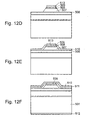
- Figs. 12A to 12F are sectional views for each step when the conventional first semiconductor laser device 500 is manufactured in accordance with the conventional method, respectively.
- an metal organic vapor phased growing method such as an MOVPE (Metal Organic Vapor Phase Epixtaxy) method, an MOCVD (Metal-Organic Chemical Vapor Deposition) method or the like, is used to epitaxially grow the buffer layer 502, the n-AlGaInP n-type clad layer 503, the GaInP superlattice active layer 504, the p-AlGaInP first p-type clad layer 505, the GaInP etching stop layer 506, the p-AlGaInP second clad layer 507, the GaInP protective layer 508 and the p-GaAs contact layer 509, sequentially on the n-GaAs substrate 501, thereby forming the lamination layer body having double hetero-structure.
- MOVPE Metal Organic Vapor Phase Epixtaxy
- MOCVD Metal-Organic Chemical Vapor Deposition
- Si and Se are used on the n-side, and Zn, Mg, Be and the like are used on the p-side.
- an SiO 2 film 513' is formed on the p-GaAs contact layer 509 of the formed lamination layer body, for example, by using a plasma CVD method.
- a resist film is formed on the SiO 2 film 513' and patterned by photographic etching, thereby forming a stripe-shaped resist mask 514.
- the resist mask 514 is used as a mask, and the SiO 2 film 513' is etched, thereby forming a stripe-shaped SiO 2 film 513.
- this stripe-shaped SiO 2 film 513 is used as a mask, and the p-GaAs contact layer 509, the GaInP protective layer 508 and the p-AlGaInP second clad layer 507 are etched and processed into the stripe-shaped ridge.
- etchant that can selectively remove this, for example, phosphoric-acid-based etchant is used to carry out a wet etching.
- the GaInP protective layer 508 is provided, the progress of the etching is stopped there, and since the p-AlGaInP second clad layer 507 is not exposed in air, it is not oxidized.
- the wet etching that uses, for example, hydrochloric-acid-based etchant is performed.
- the etching is performed in a period longer than necessary, even the p-AlGaInP second clad layer 507 and the GaInP etching stop layer 506 are etched.
- the control of the etching period is required.
- the GaInP protective layer 508 is etched, at the same time, the p-AlGaInP second clad layers 507 on both flanks of the p-GaAs contact layer 509 are etched more or less. However, it does not reach the GaInP etching stop layer 506.
- the p-AlGaInP second clad layer 507 left when the GaInP protective layer 508 is etched is etched, for example, by using sulfuric-acid-based etchant.
- the etching is stopped when the GaInP etching stop layer 506 is exposed, because the GaInP etching stop layer 506 is provided.
- the flow of this method proceeds to a second epitaxial growing step.
- the stripe-shaped SiO 2 film 513 is used as a selective growth mask, and the metal-organic vapor phased growing method such as the MOVPE method, the MOCVD method or the like is applied to epitaxially grow the n-GaAs current blocking layer 510 on the GaInP etching stop layer 506 on the slope ridge sides and ridge flanks.
- the stripe-shaped SiO 2 film 513 is etched and removed.
- the p-side electrode 511 is formed on the p-GaAs contact layer 509 and the n-GaAs current blocking layer 510, and the rear of the n-GaAs substrate 501 is polished and adjusted to a predetermined substrate thickness. Then, the n-side electrode 512 is formed on the rear. Consequently, it is possible to obtain the semiconductor wafer for the laser, which has the laminated structure shown in Fig. 11.
- this semiconductor wafer for the laser is cleaved in the ridge stripe direction and the vertical direction. Consequently, it is possible to manufacture the semiconductor laser device 500 having a pair of resonator reflection surfaces.
- the n-GaAs current blocking layer 510 can effectively carry out the current blocking function for the p-AlGaInP second clad layer 507, and the current injected from the p-side electrode 511 is narrowed by the n-GaAs current blocking layer 510 and flows into the active layer 504. If the current equal to or greater than a threshold current flows, an electron and a hole are efficiently re-combined, and the laser light is oscillated.
- the employment of the above-mentioned current confinement structure using the n-GaAs current blocking layer 510 optically increases the light loss of the semiconductor laser device, which consequently results in a problem of the increase in the oscillation threshold current.
- a refractive index of the n-GaAs current blocking layer 510 is greater than refractive indexes of the p-AlGaInP first and second clad layers 505, 507.
- the light is not absorbed by the ridge-shaped p-AlGaInP second clad layer 507, it is absorbed by the n-GaAs current blocking layer 510 of the ridge flanks of the p-AlGaInP second clad layer 507.
- the light generated by the active layer 504 indicates the motion that it is oozed into the p-AlGaInP second clad layer 507 and pushed back as it approaches the n-GaAs current blocking layer 510.
- an effective refractive index becomes low in the n-GaAs current blocking layer 510 in a laterally extending region. That is, since a refractive index difference is induced in the lateral direction of the active layer 504, a refractive index light waveguide is performed.
- the light absorption occurring in the n-GaAs current blocking layer 510 brings about the light loss on the laser oscillation, which results in a problem that the threshold current is increased.
- a method of using the effective refractive index light waveguide namely, a semiconductor laser device of an effective refractive index light waveguide type (hereafter, referred to as the conventional second semiconductor laser device) in which instead of the n-GaAs current blocking layer 510 in Fig. 13, an n-AlInP layer is provided as a current blocking layer is proposed by Ryuji Kobayashi in the International Semiconductor Laser Conference (a page 243 of the proceeding, in 1994).
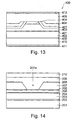
- Fig. 13 is a sectional view showing the configuration of the conventional second semiconductor laser device.
- a conventional second semiconductor laser device 400 includes the laminated structure of an n-GaAs buffer layer 406, an n-AlGaInP clad layer 402, an MQW active layer 401, a p-AlGaInP clad layer 403 and a p-GaInP cap layer 404, which are sequentially grown on an n-GaAs substrate 401, as shown in Fig. 13.
- the upper layers of the p-AlGaInP clad layer 403 and the p-GaInP cap layer 404 are processed into the stripe-shaped ridge.
- the low layer of the p-AlGaInP clad layer 403 of the ridge sides and the ridge flanks is coated with the laminated structure of an AlInP current blocking layer 407 and an n-GaAs current blocking layer 408, and further embedded with a p-GaAs contact layer 409.
- a p-side electrode 412 is formed on the p-GaAs contact layer 409, and an n-side electrode 411 is formed on a rear of the n-GaAs substrate 410, respectively.
- the AlInP current blocking layer 407 formed on the p-AlGaInP clad layer 403 of the ridge sides and of the ridge flanks functions as a current blocking layer, and simultaneously functions as a lateral light confining layer by a refractive index difference from the p-AlGaInP clad layer 403.
- the AlInP is lower in the refractive index than the AlGaInP clad layer, and there is no light absorption. Thus, it is confirmed that an inner loss is small, an oscillation threshold current can be reduced, and a light output efficiency is increased.
- n-AlInP as the current blocking layer
- Japanese Patent Application Publication No. 2001-185818 another example of employing the n-AlInP as the current blocking layer. According to this, at a first epitaxial growth step, the p-AlGaInP clad layer 403 is not made to grow, but the n-AlInP current blocking layer 407 is made to firstly grow.
- the n-AlInP current blocking layer 407 is etched to form so as to have the shape of the stripe-shaped ridge, and the p-AlGaInP clad layer 403 is made to grow at a second epitaxial growing step. This method is done in this way.
- a semiconductor laser device that employs n-AlInP as the current blocking layer is proposed. (hereafter, referred to as a conventional third semiconductor laser device) as shown in Fig. 14.
- This semiconductor laser device 200 includes the laminated structure of an n-GaAs buffer layer 202, an n-AlGaInP clad layer 203, a GaInP active layer 204, a p-AlGaInP first optical guide layer 205, a p-GaInP second optical guide layer 206, an n-AlInP current blocking layer 207 and a GaInP protective layer 208, which are sequentially grown on an n-GaAs substrate 201, as shown in Fig. 14.
- an inverted trapezoidal groove 207a is formed in the GaInP protective layer 208 and the n-AlInP current blocking layer 207 by means of etching process, and embedded with a p-AlGaInP clad layer 209. Then, a p-GaAs contact layer 210 is laminated on a p-AlGaInP clad layer 209.
- the laser light is effectively confined inside the stripe due to this refractive index difference.
- n-AlInP current blocking layer 207 is considerably larger than a band gap of the active layer 204, there is no light absorption of the laser light caused by the current blocking layer. Thus, the loss of a light waveguide can be largely reduced, thereby dropping the threshold current.
- the conventional high output semiconductor laser devices including the above-mentioned conventional second and third semiconductor laser devices have the following problems.
- a first problem of the conventional second semiconductor laser device 400 is that when the metal- organic vapor phased growing method, such as the MOVPE method, the MOCVD method and the like, is used to re-grow the AlInP current blocking layer on the ridge sides and the ridge flanks since a grid constant of the AlInP is greatly different between a flat portion of the ridge flanks and a slant portion of the ridge sides, a crystal distortion is induced in the AlInP current blocking layer. For this reason, adverse affect is induced in laser property and reliability.
- the metal- organic vapor phased growing method such as the MOVPE method, the MOCVD method and the like
- the occurrence of the crystal distortion at the time of the re-growth is because at the time of the metal-organic vapor phased growth of the AlInP current blocking layer, the fact that the grid constant of the AlInP is greatly different between the flat portion of the ridge flanks and the slant portion of the ridge sides causes the crystal planes of two kinds or more, which are different from each other, to be formed on the growth surface, thereby bringing about the segregation of raw material kind.
- diffusion coefficients of Al and In are respectively different from each other between the crystal planes, and the easiness degree when the Al and the In are taken into the crystal is different between the crystal planes, which results in the segregation of the raw material kind.
- the conventional second semiconductor laser device 400 in which as the current blocking layer, the n-AlInP layer is provided on the ridge sides and the ridge flanks, is considered to be unsuitable for the use application requiring the strict operation property, such as a high temperature operation property to a short wavelength laser device, or a high temperature high output property to a high output laser device or the like.
- a second problem of the conventional second semiconductor laser device is that since a thermal conductivity of the AlInP provided as the current blocking layer is inferior to the GaAs, the heat generated from the current which can not be converted into the light in the active layer can not be efficiently released, and therefore the temperature property of the semiconductor laser device is consequently poor.
- the conventional second semiconductor laser device employs, as the current blocking layer, the n-AlInP whose refractive index is smaller than the p-AlGaInP first and second clad layers, the light absorption in the p-AlGaInP first clad layer is reduced, and the wave guide path loss is reduced, which enables the attainment of the low threshold current and the high optical power efficiency.
- the Al composition of the n-AlInP current blocking layer is higher than the p-AlGaInP clad layer.
- the AlGaInP-based material exhibits the lower refractive index as the Al composition becomes higher.
- the AlGaInP-based material having the Al composition higher than the p-AlGaInP clad layer is used instead of the AlInP as the current blocking layer, the same effect can be expected.
- the conventional third semiconductor laser device 200 has the laser structure in which the stripe-shaped groove is formed in the n-AlInP current blocking layer 207 and the groove is embedded with the clad layer, it has the problem of difficulty to obtain the expected laser property because of the problem on the process when the n-AlInP current blocking layer 207 is etched to form the groove.
- the current blocking layer 207 is the crystal layer having the high Al composition.
- the crystal surface is immediately oxidized.
- the film thickness of the current blocking layer exposed to the air becomes 0.4 ⁇ m or more on one side.
- etchant such as concentrated sulfuric acid and the like is used in order to selectively etch the current blocking layer having the high Al composition.
- the above-mentioned gazette illustrates only the doping means, and indicates only the method of using SiO 2 insulation film with regard to the current confinement action, and does not discuss the refractive index waveguide.
- it is difficult to sufficiently carry out the light confining control of a lateral mode, and it is impossible to attain the refractive index waveguide.
- the refractive index waveguide is made to be attained by employing the AlGaInP layer having the high Al composition as the clad layer, it is desired to employ the n-AlGaInP layer having the higher Al composition ratio, for the current blocking layer.
- the n-AlGaInP layer having the high Al composition ratio is employed for the current blocking layer, as the Al composition of the p-AlGaInP clad layer is higher, it is more difficult to increase the refractive index difference between the p-AlGaInP clad layer and the AlGaInP current blocking layer. Thus since the effective refractive index becomes low, the light confinement becomes weak.
- the etching of the AlGaInP having the high Al composition is difficult as mentioned above, and there may be no process that can carry out the etching control for the stripe-shaped ridge formation.
- the guiding mechanism is determined in accordance with the longitudinal distance between the current blocking layer and the active layer to generate the light.
- the distance in order to obtain the efficient current confinement action and the high refractive index difference, it is necessary to sufficiently reduce the distance.
- the formation of the ridge structure that enables the sufficient light confinement and the efficient current confinement action is one of the most important items. To do so, the exact etching control must be carried out when the ridge is etched and processed.
- the stripe width becomes from several ten ⁇ m to several hundred ⁇ m, its NFP is desired to exhibit the lateral multi-mode profile of sharp top hat shape.
- the distance from the active layer to the current blocking layer needs to be the sufficiently small value.
- the lateral light confinement becomes weak. Consequently, even the efficiency of the current confinement action becomes worse, the NFP profile becomes a bell-shaped Gaussian type, and a light collection efficiency is worse, which results in the inconvenient laser.
- the present invention is made in view of the problems of the above-mentioned conventional techniques. It is therefore an object of the present invention to provide a high light output semiconductor laser apparatus, which solves the above-mentioned problems, and is high in the current confinement effect, small in the leak current, and favorable in the temperature property, and indicates the low threshold current, and can effectively confine the laser light to the stripe region, and is favorable in the beam profile and is high in the efficiency.
- the semiconductor laser device (hereafter, referred to as a first invention) is characterized by including: a laminated structure sequentially having at least a first conductive type AlInP clad layer, an AlGaInP-based superlattice active layer section and a second conductive type AlInP clad layer, on a first conductive type semiconductor substrate; and a current confinement structure configured by forming an upper portion made of a second conductive type compound semiconductor layer in the laminated structure into a stripe-shaped ridge, wherein an electrode on a second conductive side made of metal film extends on a ridge top surface, ridge sides and the second conductive type AlInP clad layer of ridge flanks, and directly covers the ridge top surface, the ridge sides and the second conductive type AlInP clad layer of the ridge flanks, and a carrier concentration of the second conductive type compound semiconductor layer of the ridge top surface is higher than a carrier concentration of the
- an AlGaInP-based compound semiconductor layer functioning as an etching stop layer extends on the second conductive type AlInP clad layer of the ridge flanks, and the second conductive side electrode made of the metal film extends on the ridge top surface, the ridge sides and the second conductive type AlInP clad layer of the ridge flanks through the AlGaInP-based compound semiconductor layer, and covers the ridge top surface, the ridge sides and the second conductive type AlInP clad layer of the ridge flanks through the AlGaInP-based compound semiconductor layer.
- the semiconductor laser device includes: the laminated structure having at least the AlGaInP-based superlattice active layer section, the n-AlInP clad layer which puts the superlattice active layer section between, and the p-AlInP clad layer, on the n-type semiconductor substrate; and the current confinement structure configured by forming the upper portion made of the p-type compound semiconductor layer in the laminated structure into the stripe-shaped ridge, the p-side electrode made of the metal film extends on the ridge top surface, the ridge sides and the p-AlInP clad layer of the ridge flanks, and directly covers the ridge top surface, the ridge sides and the p-AlInP clad layer of the ridge flanks, and the carrier concentration of the p-type compound semiconductor layer of the ridge top surface is higher than a carrier concentration of the p-AlInP clad layer.
- the p-side electrode made of the metal film extends on the ridge top surface, the ridge sides and the p-AlInP clad layer of the ridge flanks through the AlGaInP-based compound semiconductor layer, and directly covers the ridge top surface, the ridge sides and the AlGaInP-based compound semiconductor layer of the ridge flanks, and the carrier concentration of the p-type compound semiconductor layer of the ridge top surface is higher than the carrier concentration of the p-AlInP clad layer.
- the semiconductor laser device is attained in which the overflow of injected carriers is reduced, a leak current is small, a threshold current is low, and a temperature property is favorable.
- the carrier concentration of the second conductive type or p-type compound semiconductor layer of the ridge top surface higher than the carrier concentration of the second conductive type or p-type AlInP clad layer, ohmic junction is formed on the ridge top surface, and Schottky junction is formed on the ridge flanks.
- the current confinement action is carried out in such a way that only the ridge region serves as the current route, and the light oozed from the active layer section is reflected by the boundary plane of the p-side electrode, thereby confining the laser light to the stripe region, and reducing the light loss.
- the efficient current confinement action and the effective confinement of the laser light to the stripe region can be attained, thereby achieving the semiconductor laser of the high light output efficiency.
- the first invention to the high output semiconductor laser device of the broad area type, where the stripe width of the superlattice active layer section to which the light is guided, namely, the stripe width of the ridge is 10 ⁇ m or more, for example, the high output semiconductor laser device of 10 mW or more, it is possible to achieve the semiconductor laser device having the favorable light collection efficiency in which the lateral multi-mode profile of NFP exhibits a sharp top hat manner.
- the superlattice active layer section is constituted as an SCH (Separated Confinement Heterostructure) structure composed of at least one quantum well layer, which is sandwiched between a barrier layer and an optical guide layer, and there is a relation in which the quantum well layer is Al x Ga 1-x InP (0 ⁇ 1x ⁇ 1), and the barrier layer is Al y Ga 1-y InP (0 ⁇ y ⁇ 1), and the Al composition is (x ⁇ y).
- SCH Separatated Confinement Heterostructure
- the superlattice active layer section may be a single quantum well structure or a multiple quantum well structure having a plurality of quantum well structures.
- the superlattice active layer section is configured as the quantum well structure composed of the quantum well layer of a single layer and the optical guide layer which puts the quantum well layer between.
- the superlattice active layer section is configured as the quantum well structure composed of the quantum well layer of plural layers, which are sandwiched between the barrier layer and the optical guide layer.
- the laminated structure is a laminated structure configured by laminating: a buffer layer composed of at least one layer of an n-GaAs layer or an n-GaInP layer; an n-type clad layer made of n-AlInP; an AlGaInP-based superlattice active layer section; a first p-type clad layer made of p-AlInP; an etching stop layer made of GaInP; a second p-type clad layer made of p-AlInP; a protective layer made of GaInP; and a contact layer made of p-GaAs, sequentially on an n-GaAs substrate, and in the laminated structure, the p-AlInP second p-type clad layer and the p-GaAs contact layer are processed into the stripe-shaped ridge.
- insulating films of SiO 2 , AlN and the like may be formed on the compound semiconductor layers of the ridge sides and the ridge flanks, and the p-side electrode may be then formed on the ridge top surface exposed from the insulating film and on the insulating films of the ridge sides and the ridge flanks. Consequently, it is possible to increase the effect of suppressing the leak current, and improve the mount control property when mounting the semiconductor laser device, and the heat radiation property and the like.
- another semiconductor laser device (hereafter, referred to as the second invention) is characterized by including: a laminated structure sequentially having at least a first conductive type AlInP clad layer, an AlGaInP-based superlattice active layer section and a second conductive type AlInP clad layer, on a first conductive type semiconductor substrate; and a current confinement structure configured by forming an upper portion made of a second conductive type compound semiconductor layer in the laminated structure into a stripe-shaped ridge, wherein an insulating film extends on ridge sides and the second conductive type AlInP clad layer of ridge flanks so as to expose a ridge top surface in stripe-shaped manner, a second conductive side electrode made of metal film extends on the ridge top surface exposed from the insulating film, and further on the ridge sides and the second conductive type AlInP clad layer of the ridge flanks through the insulating film, and a carrier concentration of the second conductive type compound
- still another semiconductor laser device (hereafter, referred to as the third invention) is characterized by including: a laminated structure sequentially having at least a first conductive type AlInP clad layer, an AlGaInP-based superlattice active layer section and a second conductive type AlInP clad layer, on a first conductive type semiconductor substrate; and a current confinement structure configured by forming an upper portion made of a second conductive type compound semiconductor layer in the laminated structure into a stripe-shaped ridge, wherein an insulating film extends on the second conductive type AlInP clad layer of ridge flanks so as to expose a ridge top surface, ridge sides and the second conductive type AlInP clad layer of ridge bottom end vicinity in stripe-shaped manner, a second conductive side electrode made of metal film extends on the ridge top surface, ridge sides and the second conductive type AlInP clad layer of the ridge bottom end vicinity, which are exposed from the insulating
- a film thickness of the insulating film is from 0.05 ⁇ m to 2.00 ⁇ m.
- the insulating film for example, SiO 2 , SiN, AlN and the like are used.
- the semiconductor laser devices according to the second and third inventions have the preferable embodiments similar to the semiconductor laser device according to the first invention.
- the stripe width of the ridge is 10 ⁇ m or more.
- the carrier concentration of the second conductive type compound semiconductor layer of the ridge top surface is at least 10 times higher than the carrier concentration of the second conductive type AlInP clad layer.
- the semiconductor laser device according to the first to third inventions may be not a device unity and may be a semiconductor laser array or semiconductor laser stack having the structure arranged as array-shaped or stack-shaped manner.
- a manufacturing method of the semiconductor laser device according to the present invention (hereafter, referred to as a first invention method) is a method of manufacturing the semiconductor laser device according to the first invention, and is characterized by having:
- the first invention method has the merit that it does not require the second epitaxial growing step, because the p-side electrode is directly formed on the ridge top surface, the ridge sides and the GaInP etching stop layer of the ridge flanks without re-growing the compound semiconductor layer on the ridge flanks after the formation of the ridge.
- the step of etching and processing the protective layer made of GaInP and the second p-type clad layer made of p-AlInP uses a wet etching method, which uses acetic acid : hydrogen peroxide : hydrochloric acid, to then etch.
- the hydrogen peroxide added to the etchant when the stripe-shaped ridge is formed is desired to be adjusted to the optimal amount to the degree that the effect is not reduced. If the hydrogen peroxide becomes thin, the effect as oxidant becomes thin. Also, the time to remove As remaining on the GaInP protective layer can not be controlled, which brings about the variation in an etching period, which consequently disables the process that is favorable in the reproducibility.
- a manufacturing method of another semiconductor laser device according to the present invention (hereafter, referred to as a second invention method) is a method of manufacturing the semiconductor laser device according to the second invention, and is characterized by having:
- the step of etching the insulating film and exposing ridge top surface further exposes the GaInP etching stop layer of the ridge bottom end vicinity and the ridge sides
- the step of forming the p-side electrode forms the metal film constituting the p-side electrode, on the p-GaAs contact layer of the exposed ridge top surface, the ridge sides and the GaInP etching stop layer of the ridge bottom end vicinity, and further forms on the GaInP etching stop layer of the ridge flanks through the insulating film.
- this has the configuration that the superlattice active layer section is sandwiched between the n-AlInP clad layer and the p-AlInP first clad layer and that the p-side electrode directly covers the ridge top surface, the slant ridge sides and the compound semiconductor layer of the ridge flanks. Consequently, the semiconductor laser device according to the present invention can achieve the semiconductor laser device of the high light output efficiency, which has the structure of high current confinement effect, and is small in the leak current, and favorable in the temperature property, and low in the leak current and can effectively confine the laser light to the stripe region, and is favorable in the beam profile.
- the first invention method attains the manufacturing method preferable for manufacturing the semiconductor laser device according to the first invention.
- the first invention method has the merit that it does not require the second epitaxial growing step, because the p-side electrode is directly formed on the GaInP etching stop layer of the ridge flanks, the ridge sides and the ridge top surface, without re-growing the compound semiconductor layer on the ridge flanks after the formation of the ridge.
- the second and third inventions it is possible to consequently increase the effect of suppressing the leak current, in addition to the effect of the first invention, and improve the mount control property when mounting the semiconductor laser device, and the heat radiation property and the like.
- this has the effect similar to the first invention method, and achieves the manufacturing method preferable for manufacturing the semiconductor laser devices according to the second and third inventions.
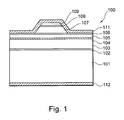
- Fig. 1 is a sectional view showing the configuration of the semiconductor laser device in this embodiment.
- a semiconductor laser device 100 in this embodiment includes the laminated structure of a buffer layer 102, a clad layer 103 made of n-Al 0.5 In 0.5 P, a superlattice active layer section 104, a first clad layer 105 made of p-Al 0.5 In 0.5 P, an etching stop layer 106 made of GaInP, a second clad layer 107 made of p-Al 0.5 In 0.5 P, a protective layer 108 made of GaInP and a contact layer 109 made of p-GaAs, which are sequentially grown on an n-GaAs substrate 101, as shown in Fig. 1.
- the buffer layer 102 is a buffer layer composed of at least one of an n-GaAs layer or an n-GaInP layer.
- the p-AlInP second clad layer 107, the GaInP protective layer 108 and the p-GaAs contact layer 109 are processed into a stripe-shaped ridge whose ridge width is 60 ⁇ m.
- a p-side electrode 111 is directly coated and formed on the GaInP etching stop layer 106 of ridge top surface, slant ridge sides and ridge flanks, and an n-side electrode 112 is formed on the rear of the n-GaAs substrate 101.
- the superlattice active layer section 104 is constituted as the SCH (Separated Confinement Heterostructure) structure composed of at least one layer of a quantum well layer, which is sandwiched between a barrier layer and an optical guide layer.
- the Al composition has the relation of (x ⁇ y).
- the superlattice active layer section 104 is formed as SQW (Single Quantum Well) structure.
- a film thickness of the buffer layer 102 is 0.03 ⁇ m and a film thickness of the n-AlInP n-type clad layer 103 is 2.00 ⁇ m
- the optical guide layer is 0.12 ⁇ m and the quantum well layer is 12 nm
- a layer thickness of the p-AlInP first p-type clad layer 105 is 0.40 ⁇ m
- a layer thickness of the GaInP etching stop layer 106 is 15 nm
- a layer thickness of the p-AlInP second p-type clad layer 107 is 1.6 ⁇ m
- a layer thickness of the GaInP protective layer 108 is 30 nm
- a layer thickness of the p-GaAs contact layer 109 is 0.26 ⁇ m.
- a carrier concentration of the p-GaAs contact layer 109 of the ridge top surface is 2 to 3 ⁇ 10 19 cm -3 , and higher than carrier concentrations 1 to 2 ⁇ 10 18 cm -3 of the p-AlInP first p-type clad layer 105 and the p-AlInP second p-type clad layer 107.
- the p-side electrode 111 is configured as the multilayer film in which a Ti film having a layer thickness of 0.05 ⁇ m, a Pt film of 0.1 ⁇ m and an Au film of 0.2 ⁇ m are deposited on the p-GaAs contact layer 109.
- the ridge height becomes 1.89 ⁇ m.
- the efficient current confinement action is carried out, and the light oozed from the superlattice active layer section 104 is reflected by the boundary plane of the p-side electrode 111. Consequently, the light loss is reduced, which enables the laser light to be effectively confined inside a stripe region.
- the p-side electrode 111 is also evaporated on the GaInP etching stop layer 106 on the ridge sides and the ridge flanks, a p-type dopant concentration is thin on this junction plane, which leads to Schottky junction so that the current does not flow.
- the current is injected from the p-side electrode 111, and flows through the region of the p-GaAs contact layer 109 in which the p-type dopant concentration on the ridge top surface is high, and arrives at the superlattice active layer section 104.
- the semiconductor laser device 100 in this embodiment is configured such that it has the structure whose current confinement effect is high, and such that the light oozed from the superlattice active layer section 104 is reflected by the boundary plane between the p-side electrode 111 and the GaInP etching stop layer 106, and such that the light loss is consequently reduced which enables the laser light to be effectively confined inside the stripe region.
- the superlattice active layer section 104 is defined as the SQW (Single Quantum Well) structure, and with regard to the layer thickness of the SCH active layer structure, the optical guide layer is 0.12 ⁇ m, and the quantum well layer is 12 nm.
- SQW Single Quantum Well
- the quantum well layer is 12 nm.
- FIG. 2A to 2F are sectional views for each step when the above-mentioned semiconductor laser device 100 is manufactured in accordance with the method in this embodiment, respectively.
- the metal-organic vapor phased growing method such as the MOVPE method, the MOCVD method or the like, is used to sequentially epitaxially grow a buffer layer 102, an n-AlInP n-type clad layer 103, a superlattice active layer section 104, a p-AlInP first p-type clad layer 105, a GaInP etching stop layer 106, a p-AlInP second p-type clad layer 107, a GaInP protective layer 108 and a p-GaAs contact layer 109, on a n-GaAs substrate 101, thereby forming a lamination layer body having the double hetero-structure.
- the MOVPE method the MOCVD method or the like
- the buffer layer 102 is composed of at least one layer of the n-GaAs layer and the n-GaInP layer.
- Si and Se are used on the n-side
- Zn, Mg, Be and the like are used on the p-side.
- a resist film is formed on the p-GaAs contact layer 109 of the formed lamination layer body, and patterned by the photographic etching, thereby forming a stripe-shaped resist mask 110.
- the p-GaAs contact layer 109 is etched and processed into the stripe-shaped ridge, and the GaInP protective layer 108 is exposed.
- the etchant that can selectively remove the p-GaAs for example, the phosphoric-acid-based etchant is used to carry out the etching.
- the phosphoric-acid-based etchant is used to etch the p-GaAs contact layer 109, the progress of the etching is stopped in the GaInP protective layer 108, and the p-AlInP second p-type clad layer 107 is not exposed in air. Thus, it is not oxidized.
- the GaInP protective layer 108 and the p-AlInP second p-type clad layer 107 are etched.
- the etchant for example, the hydrochloric-acid-based etchant is used.
- the GaInP protective layer 108 is quickly removed at the moment when the lamination layer body is dipped into the etchant, and the etching of the p-AlInP second p-type clad layer 107 is then started.
- the etching speed of the AlInP is faster than the GaInP that is the protective layer 108.
- the stirring is not performed, the permeation of the etchant is small, and the etching speed becomes slower as the etching time elapses.
- the apparent etchant concentration on a wafer surface is thin. Thus, the selectivity is exhibited.
- the p-AlInP second p-type clad layer 107 is removed to expose the GaInP etching stop layer 106.
- the p-AlInP second p-type clad layer 107 remains on the region away from the ridge.
- the current confinement action and the light confinement are carried out only in the ridge vicinity region.
- the p-AlInP second p-type clad layer 107 remains on the region away from the ridge, there is no case that a problem is induced in the laser property.
- the resist mask 110 begins to be eroded by the etchant.
- the p-GaAs contact layer 109 that is not eroded by the etchant acts the role of the mask, there is no problem on the etching control.
- the stripe-shaped resist mask 110 is removed to expose the p-GaAs contact layer 109.
- n-GaAs substrate 101 is polished and adjusted to a predetermined substrate thickness, the n-side electrode 112 is formed on the substrate rear. Consequently, it is possible to obtain the semiconductor wafer for the laser having the structure shown in Fig. 1.
- This embodiment uses the etchant composed of acetic acid : hydrogen peroxide : hydrochloric acid, and carries out the wet etching, and consequently forms the ridge.
- the action of the above-mentioned etching mechanism makes the control of the ridge shape easier.
- the respective compound semiconductor layers are epitaxially grown by using the metal-organic vapor phased growing method, such as the MOVEP method, the MOCVD method or the like.
- the metal-organic vapor phased growing method such as the MOVEP method, the MOCVD method or the like.
- the film may be formed, for example, by using an MBE (Molecular Beam Epitaxy) method or the like.
- this embodiment is designed such that a layer thickness of the p-AlInP first p-type clad layer 105 is 0.40 ⁇ m, a layer thickness of the GaInP etching stop layer 106 is 15 nm, and a layer thickness of the p-AlInP second p-type clad layer 107 is 1.6 ⁇ m.
- any layer structure may be designed.
- the clad layer structure different from this embodiment is employed in designing the lateral radiation angle property and the like, on the process, it is obviously allowable to change the concentration of acetic acid : hydrogen peroxide : hydrochloric acid and the etching period so as to make the etching control easier.
- the GaInP etching stop layer 106 when the GaInP etching stop layer 106 is exposed, the etching is stopped. Then, on the top surface thereof, the p-side electrode 111 is evaporated on the entire surface of the ridge top surface, the ridge sides and the GaInP etching stop layer 106 of the ridge flanks.
- it may be configured such that after the p-AlInP second lad layer 107 is etched, the GaInP etching stop layer 106 is further removed and the p-AlInP first clad layer 105 is exposed and the p-side electrode 111 is formed thereon.
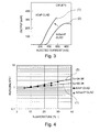
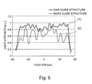
- the semiconductor laser device 100 of single stripe manufactured in accordance with the method in this embodiment the light output - current property, the property temperature and the NFP are measured, and a graph (1) of Fig. 3, a graph (1) of Fig. 4 and a graph (1) of Fig. 5 are respectively obtained.
- a horizontal axis indicates a temperature
- a vertical axis indicates Ith(Ta)/Ith(10°C).
- the Ith(Ta) is an oscillation threshold current at a time of a measurement temperature Ta °C
- the Ith(10°C) is an oscillation threshold current at a time of a measurement temperature of 10 °C.
- the graph (2) of Fig. 3 is the light output - current property of the above-mentioned conventional first semiconductor laser device 500 in which the AlGaInP serves as the clad layer.
- the semiconductor laser device 100 in this embodiment indicates the favorable light output - current property, which is low in the threshold current, as compared with the semiconductor laser device in which the AlGaInP serves as the clad layer.
- the graph (2) of Fig. 4 is the temperature property of the above-mentioned conventional first semiconductor laser device 500 in which the AlGaInP serves as the clad layer.
- the value of the To is high, and the temperature property is favorable.
- the graph (2) of Fig. 5 is the measurement result of NFP of a gain guide type semiconductor laser device manufactured as a referential example.
- the semiconductor laser device of the referential example is the gain guide type semiconductor laser device having a laminated structure shown in Fig. 6.
- the film thicknesses and compositions of the respective compound semiconductor layers and the p-side electrode are equal to the semiconductor laser device 100 except the SiO 2 film 113.
- the NFP of the semiconductor laser device 100 in this embodiment indicates the NFP of the top hat type that is sharp and favorable.
- the NFP of the semiconductor laser device of the referential example indicates the multimodal property, and this is not preferred as the high output semiconductor laser device.
- This embodiment is one example of an embodiment of a semiconductor laser device according to a second invention
- Fig. 7 is a sectional view showing the configuration of the semiconductor laser device in this embodiment.
- a semiconductor laser device 600 in this embodiment has the configuration equal to the configuration of the semiconductor laser device 100 in the first embodiment, except that the ridge sides and the ridge flanks contain insulating films, and the p-side electrode is extended to the ridge sides and the ridge flanks through the insulating films, in addition to the ridge top surface, as shown in Fig. 7.
- the same symbols are given to the portions equal to Fig. 1, among the portions shown in Fig. 7.
- the semiconductor laser device 600 in this embodiment includes the laminated structure of a buffer layer 102, a clad layer 103 made of n-Al 0.5 In 0.5 P, a superlattice active layer section 104, a first clad layer 105 made of p-Al 0.5 In 0.5 P, an etching stop layer 106 made of GaInP, a second clad layer 107 made of p-Al 0.5 In 0.5 P, a protective layer 108 made of GaInP and a contact layer 109 made of p-GaAs, which are sequentially grown on an n-GaAs substrate 101, similarly to the semiconductor laser device 100 in the first embodiment.
- the buffer layer 102 is a buffer layer composed of at least one of an n-GaAs layer or n n-GaInP layer.
- the p-AlInP second clad layer 107, the GaInP protective layer 108 and the p-GaAs contact layer 109 are processed into a stripe-shaped ridge whose ridge width is 60 ⁇ m.
- an insulating film 602 having a film thickness of 0.25 ⁇ m is formed on the ridge sides and the GaInP etching stop layer 106 of the ridge flanks except the ridge top surface, and the p-GaAs contact layer 109 is exposed through the opening of the ridge top surface.
- SiO 2 , SiN, AlN and the like are used, as the insulating film 602.
- a p-side electrode 604 is formed on the p-GaAs contact layer 109 through an opening of the insulating film 602, and further formed on the ridge sides and the GaInP etching stop layer 106 of the ridge flanks through the insulating film 602.
- the n-side electrode 112 is formed on the rear of the n-GaAs substrate 101.
- the superlattice active layer section 104 is constituted as the SCH (Separated Confinement Heterostructure) structure composed of at least one layer of the quantum well layer, which is sandwiched between the barrier layer and the optical guide layer.
- the Al composition has the relation of (x ⁇ y).
- the superlattice active layer section 104 formed as the SQW (Single Quantum Well) structure.
- the film thickness of the buffer layer 102 is 0.03 ⁇ m and the film thickness of the n-AlInP n-type clad layer 103 is 2.00 ⁇ m
- the optical guide layer is 0.12 ⁇ m and the quantum well layer is 12 nm
- the layer thickness of the p-AlInP first p-type clad layer 105 is 0.40 ⁇ m
- the layer thickness of the GaInP etching stop layer 106 is 15 nm
- the layer thickness of the p-AlInP second p-type clad layer 107 is 1.6 ⁇ m
- the layer thickness of the GaInP protective layer 108 is 30 nm
- the layer thickness of the p-GaAs contact layer 109 is 0.26 ⁇ m.
- the carrier concentration of the p-GaAs contact layer 109 of the ridge top surface is 2 to 3 ⁇ 10 19 cm -3 , and higher than the carrier concentrations 1 to 2 ⁇ 10 18 cm -3 of the p-AlInP first p-type clad layer 105 and the p-AlInP second p-type clad layer 107.
- the p-side electrode 111 is configured as the multilayer film in which a Ti film having a layer thickness of 0.05 ⁇ m, a Pt film of 0.1 ⁇ m and an Au film of 0.2 ⁇ m are deposited on the insulating film 602 and the p-GaAs contact layer 109.
- the ridge height becomes 1.89 ⁇ m.
- the current injected into the p-GaAs contact layer 109 is current-narrowed in the region of the p-AlInP second p-type clad layer 107 formed into the stripe-shaped ridge, and sent to the superlattice active layer section 104, and generates the laser oscillation.
- the efficient current confinement action is carried out, and the light oozed from the superlattice active layer section 104 is reflected by the boundary plane of the p-side electrode 111. Consequently, the light loss is reduced, which enables the laser light to be effectively confined inside the stripe region.
- the p-side electrode 111 is also evaporated on the ridge sides and the GaInP etching stop layer 106 of the ridge flanks, in addition to the interposition through the insulating film 602, the p-type dopant concentration is thin on this junction plane, which leads to the Schottky junction so that the current does not flow.
- the current is injected from the p-side electrode 111, and flows through the region of the p-GaAs contact layer 109 in which the p-type dopant concentration of the ridge top surface is high, and arrives at the superlattice active layer section 104.
- the semiconductor laser device 600 in this embodiment is designed such that it has the structure whose current confinement effect is high, and the light oozed from the superlattice active layer section 104 is reflected by the boundary plane between the p-side electrode 111 and the GaInP etching stop layer 106, and the light loss is consequently reduced which enables the laser light to be effectively confined inside the stripe region.
- the insulating film 602 is provided, it is possible to increase the effect of suppressing the leak current, and improve the mount control property when mounting the semiconductor laser device, and the heat radiation property and the like.
- the superlattice active layer section 104 is defined as the SQW (Single Quantum Well) structure, and with regard to the layer thickness of the SCH active layer structure, the optical guide layer is 0.12 ⁇ m, and the quantum well layer is 12 nm.
- SQW Single Quantum Well
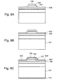
- FIG. 8A to 8C are sectional views for each step when the above-mentioned semiconductor laser device 600 is manufactured in accordance with the method in this embodiment, respectively.
- the same symbols are given to the portions equal to Figs. 2A to 2F, among the portions shown in Figs. 8A to 8C.
- the metal-organic vapor phased growing method such as the MOVPE method, the MOCVD method or the like, is used to sequentially epitaxially grow a buffer layer 102, an n-AlInP n-type clad layer 103, a superlattice active layer section 104, a p-AlInP first p-type clad layer 105, a GaInP etching stop layer 106, a p-AIInP second p-type clad layer 107, a GaInP protective layer 108 and a p-GaAs contact layer 109, on n n-GaAs substrate 101, thereby generating a lamination layer body having the double hetero-structure.
- the MOVPE method the MOCVD method or the like
- the buffer layer 102 is composed of at least one layer of an n-GaAs layer of a n-GaInP layer.
- Si and Se are used on the n-side
- Zn, Mg, Be and the like are used on the p-side.
- the resist film is formed on the p-GaAs contact layer 109 of the formed lamination layer body, and patterned by the photographic etching, thereby forming the stripe-shaped resist mask 110 (refer to Fig. 2B). Then, from above the resist mask 110, the p-GaAs contact layer 109 is etched and processed into the stripe-shaped ridge, and the GaInP protective layer 108 is exposed. In etching, the etchant that can selectively remove the p-GaAs, for example, the phosphoric-acid-based etchant is used to carry out the etching.
- the phosphoric-acid-based etchant is used to etch the p-GaAs contact layer 109, the progress of the etching is stopped in the GaInP protective layer 108, and the p-AlInP second p-type clad layer 107 is not exposed in the air. Thus, it is not oxidized.
- the GaInP protective layer 108 and the p-AlInP second p-type clad layer 107 are etched.
- the etchant for example, the hydrochloric-acid-based etchant is used.
- the GaInP protective layer 108 is quickly removed at the moment when the lamination layer body is dipped into the etchant, and the etching of the p-AlInP second p-type clad layer 107 is then started.
- the etching speed of the AlInP is faster than the GaInP that is the protective layer 108.
- the stirring is not performed, the permeation of the etchant is small, and the etching speed becomes slower as the etching time elapses.
- the apparent etchant concentration on the wafer surface is thin. Thus, the selectivity is exhibited.
- the p-AlInP second p-type clad layer 107 is removed to expose the GaInP etching stop layer 106.
- the p-AlInP second p-type clad layer 107 remains on the region away from the ridge.
- the current confinement action and the light confinement are carried out only in the ridge vicinity region.
- the p-AlInP second p-type clad layer 107 remains on the region away from the ridge, there is no case that a problem is induced in the laser property.
- the resist mask 110 begins to be eroded by the etchant.
- the p-GaAs contact layer 109 that is not eroded by the etchant acts the role of the mask, there is no problem on the etching control.
- the stripe-shaped resist mask 110 is removed to expose the p-GaAs contact layer 109.
- the insulating film 602 is formed on the entire surface of the ridge top surface, the ridge sides and the GaInP etching stop layer 106 of the ridge flanks.
- the insulating film 602 of the ridge top surface is etched to expose the p-GaAs contact layer 109.
- the Ti/Pt/Au multilayer film is evaporated on the entire surface of the p-GaAs contact layer 109 of the ridge top surface and on the insulating film 602 of the ridge sides and the ridge flanks, and the p-side electrode 604 is then formed.
- n-GaAs substrate 101 After the rear of the n-GaAs substrate 101 is polished and adjusted to the predetermined substrate thickness, an n-side electrode 112 is formed on the substrate rear. Consequently, it is possible to obtain the semiconductor wafer for the laser having the structure shown in Fig. 7.
- the semiconductor laser device 600 having a pair of resonator reflection surfaces.
- This embodiment uses the etchant composed of acetic acid : hydrogen peroxide : hydrochloric acid, and carries out the wet etching, and forms the ridge.
- the action of the above-mentioned etching mechanism makes the control of the ridge shape easier.
- the respective compound semiconductor layers are epitaxially grown by using the metal-organic vapor phased growing method, such as the MOVEP method, the MOCVD method or the like.
- the metal-organic vapor phased growing method such as the MOVEP method, the MOCVD method or the like.
- the film may be formed, for example, by using the MBE (Molecular Beam Epitaxy) method or the like.
- this embodiment is designed such that the layer thickness of the p-AlInP first p-type clad layer 105 is 0.40 ⁇ m, the layer thickness of the GaInP etching stop layer 106 is 15 nm, and the layer thickness of the p-AlInP second p-type clad layer 107 is 1.6 ⁇ m.
- any layer structure may be designed.
- the clad layer structure different from this embodiment is employed in designing the lateral radiation angle property and the like, on the process, it is obviously allowable to change the concentration of acetic acid : hydrogen peroxide : hydrochloric acid and the etching period so as to make the etching control easier.
- the GaInP etching stop layer 106 when the GaInP etching stop layer 106 is exposed, the etching is stopped. Then, on the top surface thereof, the p-side electrode 111 is evaporated on the entire surface of the ridge top surface, the ridge sides and the GaInP etching stop layer 106 of the ridge flanks.
- it may be configured such that after the p-AlInP second clad layer 107 is etched, the GaInP etching stop layer 106 is further removed and the p-AlInP first clad layer 105 is exposed and the insulating film 602 is formed thereon.
- This embodiment is one example of an embodiment of a semiconductor laser device according to a third invention
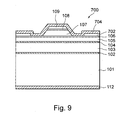
- Fig. 9 is a sectional view showing the configuration of the semiconductor laser device in this embodiment.
- a semiconductor laser device 700 in this embodiment has the configuration equal to the configuration of the semiconductor laser device 600 in the third embodiment, except that only a ridge sides contains an insulating film, and a part of a p-side electrode is provided through the insulating film.
- the same symbols are given to the portions equal to Fig. 7, among the portions shown in Fig. 9.
- the semiconductor laser device 700 in this embodiment includes the laminated structure of a buffer layer 102, a clad layer 103 made of n-Al 0.5 In 0.5 P, a superlattice active layer section 104, a first clad layer 105 made of p-Al 0.5 In 0.5 P, an etching stop layer 106 made of GaInP, a second clad layer 107 made of p-Al 0.5 In 0.5 P, a protective layer 108 made of GaInP and a contact layer 109 made of p-GaAs, which are sequentially grown on an n-GaAs substrate 101, similarly to the semiconductor laser device 600 in the sixth embodiment.
- the buffer layer 102 is a buffer layer composed of at least one of an n-GaAs layer or an n-GaInP layer.
- the p-AlInP second clad layer 107, the GaInP protective layer 108 and the p-GaAs contact layer 109 are processed into a stripe-shaped ridge whose ridge width is 60 ⁇ m.
- a carrier concentration of the p-GaAs contact layer 109 of the ridge top surface is 2 to 3 ⁇ 10 19 cm -3 , and higher than carrier concentrations 1 to 2 ⁇ 10 18 cm -3 of the p-AlInP first p-type clad layer 105 and the p-AlInP second p-type clad layer 107.
- an insulating film 702 is formed only on the GaInP etching stop layer 106 in the region separated from a ridge bottom end, and is not formed on the ridge top surface, the ridge sides and the ridge bottom end vicinity. Then, it serves as an opening, which causes the p-GaAs contact layer 109 of the ridge top surface and the GaInP etching stop layer 106 of the ridge sides and the ridge bottom end vicinity to be exposed in the stripe-shaped manner.
- a film thickness of the insulating film 702 is 0.25 ⁇ m.
- SiO 2 , SiN, AIN and the like are used, as the insulating film 702.
- a p-side electrode 704 is formed on the p-GaAs contact layer 109, which is exposed from the opening of the insulating film 702, and on the GaInP etching stop layer 106 of the ridge sides and the ridge bottom end vicinity, and further formed on the GaInP etching stop layer 106 of the ridge flanks through the insulating film 602.
- an n-side electrode 112 is formed on the rear of the n-GaAs substrate 101.
- the insulating film 702 is provided, it is possible to increase the effect of suppressing the leak current, and improve the mount control property when mounting the semiconductor laser device, and the heat radiation property and the like
- FIG. 10A to 10C are sectional views of the main steps when the above-mentioned semiconductor laser device 700 is manufactured in accordance with the method in this embodiment, respectively.
- the same symbols are given to the portions equal to Figs. 8A to 8C, among the portions shown in Figs. 10A to 10C.
- the metal-organic vapor phased growing method such as the MOVPE method, the MOCVD method or the like, is used to sequentially epitaxially grow the buffer layer 102, the n-type clad layer 103 made of n-AlInP, the superlattice active layer section 104, the p-AlInP first p-type clad layer 105, the GaInP etching stop layer 106, the p-AlInP second p-type clad layer 107, the GaInP protective layer 108 and the p-GaAs contact layer 109, on the n-GaAs substrate 101, thereby forming a lamination layer body having the double hetero-structure.
- the metal-organic vapor phased growing method such as the MOVPE method, the MOCVD method or the like
- the buffer layer 102 is composed of at least one layer of an n-GaAs layer or an n-GaInP layer.
- Si and Se are used on the n-side
- Zn, Mg, Be and the like are used on the p-side.
- a resist film is formed on the p-GaAs contact layer 109 of the formed lamination layer body, and patterned by the photographic etching, thereby forming a stripe-shaped resist mask 110 (refer to Fig. 2B). Then, from above the resist mask 110, the p-GaAs contact layer 109 is etched and processed into the stripe-shaped ridge, and the GaInP protective layer 108 is exposed. In etching, the etchant that can selectively remove the p-GaAs, for example, the phosphoric-acid-based etchant is used to carry out the etching.
- the phosphoric-acid-based etchant is used to etch the p-GaAs contact layer 109, the progress of the etching is stopped in the GaInP protective layer 108, and the p-AlInP second p-type clad layer 107 is not exposed in the air. Thus, it is not oxidized.
- the GaInP protective layer 108 and the p-AlInP second p-type clad layer 107 are etched.
- the etchant for example, the hydrochloric-acid-based etchant is used.
- the GaInP protective layer 108 is quickly removed at the moment when the lamination layer body is dipped into the etchant, and the etching of the p-AlInP second p-type clad layer 107 is then started.
- the etching speed of the AlInP is faster than the GaInP that is the protective layer 108.
- the stirring is not performed, the permeation of the etchant is small, and the etching speed becomes slower as the etching time elapses.
- the apparent etchant concentration on the wafer surface is thin. Thus, the selectivity is exhibited.
- the p-AlInP second p-type clad layer 107 is removed to expose the GaInP etching stop layer 106.
- the p-AlInP second p-type clad layer 107 remains on the region away from the ridge.
- the current confinement action and the light confinement are carried out only in the ridge vicinity region.
- the p-AlInP second p-type clad layer 107 remains on the region away from the ridge, there is no case that a problem is induced in the laser property.
- the resist mask 110 begins to be eroded by the etchant.
- the p-GaAs contact layer 109 that is not eroded by the etchant acts the role of the mask, there is no problem on the etching control.
- the stripe-shaped resist mask 110 is removed to expose the p-GaAs contact layer 109 (refer to Fig. 8A).
- the insulating film 702 is formed on the entire surface of the ridge top surface, the ridge sides and the GaInP etching stop layer 106 of the ridge flanks.
- the insulating film 702 of the ridge top surface, the ridge sides and the ridge bottom end vicinity is etched and removed, thereby exposing the p-GaAs contact layer 109 of the ridge top surface and the GaInP etching stop layer 106 of the ridge sides and the ridge bottom end vicinity.
- the Ti/Pt/Au multilayer film is evaporated on the p-GaAs contact layer 109 of the ridge top surface, on the GaInP etching stop layer 106 which is exposed on the ridge sides and the ridge bottom end vicinity, and on the entire surface of the insulating film 702 of the ridge flanks, and the p-side electrode 704 is formed.
- n-GaAs substrate 101 After the rear of the n-GaAs substrate 101 is polished and adjusted to the predetermined substrate thickness, an n-side electrode 112 is formed on the substrate rear. Consequently, it is possible to obtain the semiconductor wafer for the laser having the structure shown in Fig. 9.
- the semiconductor laser device 700 having a pair of resonator reflection surfaces.
- This embodiment uses the etchant composed of acetic acid : hydrogen peroxide : hydrochloric acid, and carries out the wet etching, and forms the ridge.
- the action of the above-mentioned etching mechanism makes the control of the ridge shape easier.
- the respective compound semiconductor layers are epitaxially grown by using the metal-organic vapor phased growing method, such as the MOVEP method, the MOCVD method or the like.
- the metal-organic vapor phased growing method such as the MOVEP method, the MOCVD method or the like.
- the film may be formed, for example, by using the MBE (Molecular Beam Epitaxy) method or the like.
- this embodiment is designed such that the layer thickness of the p-AlInP first p-type clad layer 105 is 0.40 ⁇ m, the layer thickness of the GaInP etching stop layer 106 is 15 nm, and the layer thickness of the p-AlInP second p-type clad layer 107 is 1.6 ⁇ m.
- any layer structure may be designed.
- the clad layer structure different from this embodiment is employed in designing the lateral radiation angle property and the like, on the process, it is obviously allowable to change the concentration of acetic acid : hydrogen peroxide : hydrochloric acid and the etching period so as to make the etching control easier.
- the GaInP etching stop layer 106 when the GaInP etching stop layer 106 is exposed, the etching is stopped. Then, on the top surface thereof, the p-side electrode 111 is evaporated on the entire surface of the ridge top surface, the ridge sides and the GaInP etching stop layer 106 of the ridge flanks.
- it may be configured such that after the p-AlInP second lad layer 107 is etched, the GaInP etching stop layer 106 is further removed and the p-AlInP first clad layer 105 is exposed and the insulating film 602 is formed thereon.
- the first to third inventions can be also applied to a semiconductor laser array or a semiconductor laser stack in which the semiconductor laser devices are arrayed in array manner or stack manner.
Landscapes
- Physics & Mathematics (AREA)
- Optics & Photonics (AREA)
- General Physics & Mathematics (AREA)
- Condensed Matter Physics & Semiconductors (AREA)
- Electromagnetism (AREA)
- Chemical & Material Sciences (AREA)
- Engineering & Computer Science (AREA)
- Nanotechnology (AREA)
- Biophysics (AREA)
- Crystallography & Structural Chemistry (AREA)
- Life Sciences & Earth Sciences (AREA)
- Geometry (AREA)
- Semiconductor Lasers (AREA)
Abstract
Description
wherein an electrode on a second conductive side made of metal film extends on a ridge top surface, ridge sides and the second conductive type AlInP clad layer of ridge flanks, and directly covers the ridge top surface, the ridge sides and the second conductive type AlInP clad layer of the ridge flanks, and
a carrier concentration of the second conductive type compound semiconductor layer of the ridge top surface is higher than a carrier concentration of the second conductive type AlInP clad layer.
the second conductive side electrode made of the metal film extends on the ridge top surface, the ridge sides and the second conductive type AlInP clad layer of the ridge flanks through the AlGaInP-based compound semiconductor layer, and covers the ridge top surface, the ridge sides and the second conductive type AlInP clad layer of the ridge flanks through the AlGaInP-based compound semiconductor layer.
the p-side electrode made of the metal film extends on the ridge top surface, the ridge sides and the p-AlInP clad layer of the ridge flanks, and directly covers the ridge top surface, the ridge sides and the p-AlInP clad layer of the ridge flanks, and
the carrier concentration of the p-type compound semiconductor layer of the ridge top surface is higher than a carrier concentration of the p-AlInP clad layer.
the carrier concentration of the p-type compound semiconductor layer of the ridge top surface is higher than the carrier concentration of the p-AlInP clad layer.
in the laminated structure, the p-AlInP second p-type clad layer and the p-GaAs contact layer are processed into the stripe-shaped ridge.
wherein an insulating film extends on ridge sides and the second conductive type AlInP clad layer of ridge flanks so as to expose a ridge top surface in stripe-shaped manner,
a second conductive side electrode made of metal film extends on the ridge top surface exposed from the insulating film, and further on the ridge sides and the second conductive type AlInP clad layer of the ridge flanks through the insulating film, and
a carrier concentration of the second conductive type compound semiconductor layer of the ridge top surface is higher than a carrier concentration of the second conductive type AlInP clad layer.
wherein an insulating film extends on the second conductive type AlInP clad layer of ridge flanks so as to expose a ridge top surface, ridge sides and the second conductive type AlInP clad layer of ridge bottom end vicinity in stripe-shaped manner,
a second conductive side electrode made of metal film extends on the ridge top surface, ridge sides and the second conductive type AlInP clad layer of the ridge bottom end vicinity, which are exposed from the insulating film, and extends further on the second conductive type AlInP clad layer of the ridge flanks through the insulating film, and
a carrier concentration of the second conductive type compound semiconductor layer of the ridge top surface is higher than a carrier concentration of the second conductive type AlInP clad layer.
Claims (28)
- A semiconductor laser device characterized by comprising:a laminated structure sequentially having at least a first conductive type AlInP clad layer, an AlGaInP-based superlattice active layer section and a second conductive type AlInP clad layer, on a first conductive type semiconductor substrate; andwherein an electrode on a second conductive side made of metal film extends on a ridge top surface, ridge sides and the second conductive type AlInP clad layer of ridge flanks, and directly covers the ridge top surface, the ridge sides and the second conductive type AlInP clad layer of the ridge flanks; anda current confinement structure configured by forming an upper portion made of a second conductive type compound semiconductor layer in the laminated structure into a stripe-shaped ridge;a carrier concentration of the second conductive type compound semiconductor layer of the ridge top surface is higher than a carrier concentration of the second conductive type AlInP clad layer.
- The semiconductor laser device according to claim 1,
characterized in that:an AlGaInP-based compound semiconductor layer functioning as an etching stop layer extends on the second conductive type AlInP clad layer of the ridge flanks, andthe second conductive side electrode made of the metal film extends on the ridge top surface, the ridge sides and the AlGaInP-based compound semiconductor layer, and directly covers the ridge top surface, the ridge sides and the AlGaInP-based compound semiconductor layer. - The semiconductor laser device according to claim 1 or 2, characterized in that the first conductive type is an n-type, the second conductive type is a p-type, and the second conductive side electrode is a p-side electrode.
- The semiconductor laser device according to claim 3, characterized in that a stripe width of the ridge is 10 µm or more.
- The semiconductor laser device according to claim 4,
characterized in that:a laminated structure is a laminated structure configured by laminating: a buffer layer composed of at least one layer of an n-GaAs layer or an n-GaInP layer; an n-type clad layer made of n-AlInP; an AlGaInP-based superlattice active layer section; a first p-type clad layer made of p-AlInP; an etching stop layer made of GaInP; a second p-type clad layer made of p-AlInP; a protective layer made of GaInP; and a contact layer made of p-GaAs, sequentially on an n-GaAs substrate, andin the laminated structure, the p-AlInP second p-type clad layer and the p-GaAs contact layer are processed into the stripe-shaped ridge, thereby configuring the current confinement structure. - The semiconductor laser device according to claim 5, characterized in that the superlattice active layer section is constituted as an SCH (Separated Confinement Heterostructure) structure composed of at least one quantum well layer, which is sandwiched between a barrier layer and an optical guide layer, and there is a relation in which the quantum well layer is AlxGa1-xInP (0≤1x<1), and the barrier layer is AlyGa1-yInP (0<y≤1), and the Al composition is (x<y).
- The semiconductor laser device according to claim 6, characterized in that the superlattice active layer section is configured as the multiple quantum well structure composed of the quantum well layer of plural layers, which is sandwiched between the barrier layer and the optical guide layer.
- A semiconductor laser device characterized by comprising:a laminated structure sequentially having at least a first conductive type AlInP clad layer, an AlGaInP-based superlattice active layer section and a second conductive type AlInP clad layer, on a first conductive type semiconductor substrate; anda current confinement structure configured by forming an upper portion made of a second conductive type compound semiconductor layer in the laminated structure into a stripe-shaped ridge,
wherein an insulating film extends on ridge sides and the second conductive type AlInP clad layer of ridge flanks, so as to expose a ridge top surface in stripe-shaped manner,a second conductive side electrode made of metal film extends on the ridge top surface exposed from the insulating film, and further on the ridge sides and the second conductive type AlInP clad layer of the ridge flanks through the insulating film, anda carrier concentration of the second conductive type compound semiconductor layer of the ridge top surface is higher than a carrier concentration of the second conductive type AlInP clad layer. - The semiconductor laser device according to claim 8, characterized in that:an AlGaInP-based compound semiconductor layer functioning as an etching stop layer extends on the second conductive type AlInP clad layer of the ridge flanks;the insulating film extends on the ridge sides and the AlGaInP-based compound semiconductor layer of the ridge flanks, so as to expose the ridge top surface; andthe second conductive side electrode made of the metal film extends on the ridge top surface exposed from the insulating film, and further on the ridge sides and the AlGaInP-based compound semiconductor layer of the ridge flanks through the insulating film.
- The semiconductor laser device according to claim 8 or 9, characterized in that the first conductive type is an n-type, the second conductive type is a p-type, and the second conductive side electrode is a p-side electrode.
- The semiconductor laser device according to claim 10, characterized in that a stripe width of the ridge is 10 µm or more.
- The semiconductor laser device according to claim 11, characterized in that:the laminated structure is a laminated structure configured by laminating: a buffer layer composed of at least one layer of an n-GaAs layer or an n-GaInP layer; an n-type clad layer made of n-AlInP; an AlGaInP-based superlattice active layer section; a first p-type clad layer made of p-AlInP; an etching stop layer made of GaInP; a second p-type clad layer made of p-AlInP; a protective layer made of GaInP; and a contact layer made of p-GaAs, sequentially on an n-GaAs substrate; andin the laminated structure, the p-AlInP second p-type clad layer and the p-GaAs contact layer are processed into the stripe-shaped ridge, thereby configuring the current confinement structure.
- The semiconductor laser device according to claim 12, characterized in that the superlattice active layer section is constituted as an SCH (Separated Confinement Heterostructure) structure composed of at least one quantum well layer, which is sandwiched between a barrier layer and an optical guide layer, and there is a relation in which the quantum well layer is AlxGa1-xInP (0≤1x<1), and the barrier layer is AlyGa1-yInP (0<y≤1), and the Al composition is (x<y).
- The semiconductor laser device according to claim 13, characterized in that the superlattice active layer section is configured as the multiple quantum well structure composed of the quantum well layer of plural layers, which is sandwiched between the barrier layer and the optical guide layer.
- A semiconductor laser device characterized by comprising:a laminated structure sequentially having at least a first conductive type AlInP clad layer, an AlGaInP-based superlattice active layer section and a second conductive type AlInP clad layer, on a first conductive type semiconductor substrate; anda current confinement structure configured by forming an upper portion made of a second conductive type compound semiconductor layer in the laminated structure into a stripe-shaped ridge;
wherein an insulating film extends on the second conductive type AlInP clad layer of ridge flanks, so as to expose a ridge top surface, ridge sides and the second conductive type AlInP clad layer of ridge bottom end vicinity in stripe-shaped manner,a second conductive side electrode made of metal film extends on the ridge top surface, the ridge sides and the second conductive type AlInP clad layer of the ridge bottom end vicinity, which are exposed from the insulating film, and further extends on the second conductive type AlInP clad layer of the ridge flanks through the insulating film, anda carrier concentration of the second conductive type compound semiconductor layer of the ridge top surface is higher than a carrier concentration of the second conductive type AlInP clad layer. - The semiconductor laser device according to claim 15, characterized in that:an AlGaInP-based compound semiconductor layer functioning as an etching stop layer extends on the second conductive type AlInP clad layer of the ridge flanks;the insulating film extends on the AlGaInP-based compound semiconductor layer of the ridge flanks, so as to expose the ridge top surface, the ridge sides and the AlGaInP-based compound semiconductor layer of ridge bottom end vicinity; andthe second conductive side electrode made of the metal film extends on the ridge top surface, the ridge sides and the AlGaInP-based compound semiconductor layer of the ridge bottom end vicinity, which are exposed from the insulating film, and further extends on the AlGaInP-based compound semiconductor layer of the ridge flanks through the insulating film.
- The semiconductor laser device according to claim 15 or 16, characterized in that the first conductive type is an n-type, the second conductive type is a p-type, and the second conductive side electrode is a p-side electrode.
- The semiconductor laser device according to claim 17, characterized in that a stripe width of the ridge is 10 µm or more.
- The semiconductor laser device according to claim 18, characterized in that the laminated structure is a laminated structure configured by laminating: a buffer layer composed of at least one layer of an n-GaAs layer or an n-GaInP layer; an n-type clad layer made of n-AlInP; an AlGaInP-based superlattice active layer section; a first p-type clad layer made of p-AlInP; an etching stop layer made of GaInP; a second p-type clad layer made of p-AlInP; a protective layer made of GaInP; and a contact layer made of p-GaAs, sequentially on an n-GaAs substrate; and
in the laminated structure, the p-AlInP second p-type clad layer and the p-GaAs contact layer are processed into the stripe-shaped ridge, thereby configuring the current confinement structure. - The semiconductor laser device according to claim 19, characterized in that the superlattice active layer section is constituted as an SCH (Separated Confinement Heterostructure) structure composed of at least one quantum well layer, which is sandwiched between a barrier layer and an optical guide layer, and there is a relation in which the quantum well layer is AlxGa1-xInP (0≤1x<1), and the barrier layer
is AlyGa1-yInP (0<y≤1), and the Al composition is (x<y). - The semiconductor laser device according to claim 20, characterized in that the superlattice active layer section is configured as a multiple quantum well structure composed of the quantum well layer of plural layers, which are sandwiched between the barrier layer and the optical guide layer.
- A manufacturing method of a semiconductor laser device, characterized by comprising:a step of sequentially epitaxial growth a buffer layer composed of at least one of an n-GaAs layer or an n-GaInP layer, an n-type clad layer made of n-AlInP, a superlattice active layer section, a first p-type clad layer made of p-AlInP, an etching stop layer made of GaInP, a second p-type clad layer made of p-AlInP, a protective layer made of GaInP, and a contact layer made of p-GaAs, on an n-GaAs substrate;a step of etching processing the p-GaAs contact layer into stripe-shaped manner;a step of processing into stripe-shaped ridge by etching the GaInP protective layer and the p-AlInP second p-type clad layer using the stripe-shaped p-GaAs contact layer as an etching mask, and exposing the GaInP etching stop layer on ridge flanks; anda step of forming a metal film constituting a p-side electrode on the p-GaAs contact layer of a ridge top surface, ridge sides and the GaInP etching stop layer of the ridge flanks.
- The manufacturing method of the semiconductor laser device according to claim 22, characterized in that the step of etching the GaInP protective layer and the p-AlInP second p-type clad layer uses a wet etching method, which uses acetic acid : hydrogen peroxide : hydrochloric acid, to then etch.
- The manufacturing method of the semiconductor laser device according to claim 22 or 23, characterized in that the p-type compound semiconductor layer is replaced by an n-type compound semiconductor layer, and the n-type compound semiconductor layer is replaced by a p-type compound semiconductor layer, namely, they are replaced by the opposite conductive types, respectively.
- A manufacturing method of a semiconductor laser device, characterized by comprising:a step of sequentially epitaxial growth a buffer layer composed of at least one of an n-GaAs layer or an n-GaInP layer, an n-type clad layer made of n-AlInP, a superlattice active layer section, a first p-type clad layer made of p-AlInP, an etching stop layer made of GaInP, a second p-type clad layer made of p-AlInP, a protective layer made of GaInP, and a contact layer made of p-GaAs, on an n-GaAs substrate;a step of etching processing the p-GaAs contact layer into stripe-shaped manner;a step of processing into stripe-shaped ridge by etching the GaInP protective layer and the p-AlInP second p-type clad layer using the stripe-shaped p-GaAs contact layer as an etching mask, and exposing the GaInP etching stop layer on ridge flanks;a step of forming an insulating film on an entire surface of the substrate;a step of etching the insulating film and exposing a ridge top surface in stripe-shaped manner; anda step of forming a metal film constituting a p-side electrode on the p-GaAs contact layer of the ridge top surface and further on the ridge sides and the GaInP etching stop layer of the ridge flanks through the insulating film.
- The manufacturing method of the semiconductor laser device according to claim 25, characterized in that:the step of etching the insulating film and exposing the ridge top surface further exposes the ridge sides and the GaInP etching stop layer of ridge bottom end vicinity; andthe step of forming the p-side electrode forms the metal film constituting the p-side electrode on the p-GaAs contact layer of the exposed ridge top surface, the ridge sides and the GaInP etching stop layer of the ridge bottom end vicinity, and further forming on the GaInP etching stop layer of the ridge flanks through the insulating film.
- The manufacturing method of the semiconductor laser device according to claim 25 or 26, characterized in that the step of etching the GaInP protective layer and the p-AlInP second p-type clad layer uses a wet etching method, which uses acetic acid : hydrogen peroxide : hydrochloric acid, to then etch.
- The manufacturing method of the semiconductor laser device according to claim 27, characterized in that the p-type compound semiconductor layer is replaced by an n-type compound semiconductor layer, and the n-type compound semiconductor layer is replaced by a p-type compound semiconductor layer, namely, they are replaced by the opposite conductive types, respectively.
Applications Claiming Priority (3)
| Application Number | Priority Date | Filing Date | Title |
|---|---|---|---|
| JP2002274492 | 2002-09-20 | ||
| JP2002274492 | 2002-09-20 | ||
| PCT/JP2003/011985 WO2004032296A1 (en) | 2002-09-20 | 2003-09-19 | Semiconductor laser device and production method therefor |
Publications (3)
| Publication Number | Publication Date |
|---|---|
| EP1555731A1 true EP1555731A1 (en) | 2005-07-20 |
| EP1555731A4 EP1555731A4 (en) | 2005-10-26 |
| EP1555731B1 EP1555731B1 (en) | 2010-04-14 |
Family
ID=32063495
Family Applications (1)
| Application Number | Title | Priority Date | Filing Date |
|---|---|---|---|
| EP03799114A Expired - Lifetime EP1555731B1 (en) | 2002-09-20 | 2003-09-19 | Semiconductor laser device and production method therefor |
Country Status (5)
| Country | Link |
|---|---|
| US (3) | US20050041712A1 (en) |
| EP (1) | EP1555731B1 (en) |
| CN (1) | CN1610995B (en) |
| DE (1) | DE60332140D1 (en) |
| WO (1) | WO2004032296A1 (en) |
Cited By (1)
| Publication number | Priority date | Publication date | Assignee | Title |
|---|---|---|---|---|
| EP2866316A1 (en) * | 2013-10-23 | 2015-04-29 | Alcatel Lucent | Thermal management of a ridge-type hybrid laser, device, and method |
Families Citing this family (14)
| Publication number | Priority date | Publication date | Assignee | Title |
|---|---|---|---|---|
| CN101233443B (en) * | 2005-07-28 | 2010-06-23 | 松下电器产业株式会社 | Laser image display |
| WO2011056675A1 (en) * | 2009-11-03 | 2011-05-12 | The Regents Of The University Of California | Superluminescent diodes by crystallographic etching |
| CN105071221A (en) * | 2015-08-26 | 2015-11-18 | 武汉电信器件有限公司 | High-speed laser chip |
| DE102015116712B4 (en) * | 2015-10-01 | 2024-11-28 | OSRAM Opto Semiconductors Gesellschaft mit beschränkter Haftung | optoelectronic component |
| CN105406359B (en) * | 2015-12-29 | 2019-06-18 | 山东华光光电子股份有限公司 | A kind of AlGaInP semiconductor laser containing highly selective corrosion barrier layer |
| CN106300012B (en) * | 2016-09-19 | 2020-02-14 | 山东华光光电子股份有限公司 | 808nm semiconductor laser containing high-selectivity corrosion barrier layer |
| CN108512031B (en) * | 2017-02-28 | 2020-02-14 | 山东华光光电子股份有限公司 | Micro-channel semiconductor laser chip structure and manufacturing method thereof |
| CN111092366B (en) * | 2018-10-23 | 2021-04-06 | 山东华光光电子股份有限公司 | Semiconductor laser with double-sided current limiting structure and preparation method |
| CN110880675A (en) * | 2019-11-25 | 2020-03-13 | 江苏华兴激光科技有限公司 | Side grating oxidation-confined structure single longitudinal mode edge emitting laser and preparation method thereof |
| JP2021097172A (en) * | 2019-12-18 | 2021-06-24 | シャープ福山レーザー株式会社 | Semiconductor laser element |
| JP7330128B2 (en) * | 2020-04-02 | 2023-08-21 | 浜松ホトニクス株式会社 | Quantum cascade laser device and quantum cascade laser device |
| JP7489814B2 (en) * | 2020-04-02 | 2024-05-24 | 浜松ホトニクス株式会社 | Quantum cascade laser element and quantum cascade laser device |
| CN114725777B (en) * | 2022-03-02 | 2025-11-07 | 山东华光光电子股份有限公司 | Semiconductor laser chip for improving wide ridge thermal lens effect |
| FR3150347A1 (en) * | 2023-06-22 | 2024-12-27 | Thales | Semiconductor optoelectronic component with improved heat dissipation |
Family Cites Families (19)
| Publication number | Priority date | Publication date | Assignee | Title |
|---|---|---|---|---|
| US4797179A (en) * | 1987-06-09 | 1989-01-10 | Lytel Corporation | Fabrication of integral lenses on LED devices |
| JPH04111375A (en) * | 1990-08-30 | 1992-04-13 | Furukawa Electric Co Ltd:The | Semiconductor laser element |
| JP2728974B2 (en) * | 1990-11-13 | 1998-03-18 | キヤノン株式会社 | Optical integrated device |
| JPH0677205A (en) * | 1992-08-26 | 1994-03-18 | Matsushita Electric Ind Co Ltd | Method for forming fine structure of compound semiconductor |
| US5523256A (en) * | 1993-07-21 | 1996-06-04 | Matsushita Electric Industrial Co., Ltd. | Method for producing a semiconductor laser |
| JPH0878775A (en) * | 1994-09-06 | 1996-03-22 | Fuji Xerox Co Ltd | Semiconductor laser device and its manufacture |
| US5832019A (en) * | 1994-11-28 | 1998-11-03 | Xerox Corporation | Index guided semiconductor laser biode with shallow selective IILD |
| JPH09139550A (en) * | 1995-11-16 | 1997-05-27 | Mitsubishi Electric Corp | Method for manufacturing semiconductor laser device and semiconductor laser device |
| US5963572A (en) * | 1995-12-28 | 1999-10-05 | Sanyo Electric Co., Ltd. | Semiconductor laser device and manufacturing method thereof |
| JP3505186B2 (en) * | 1996-06-13 | 2004-03-08 | 古河電気工業株式会社 | Semiconductor waveguide type light receiving element and method of manufacturing the same |
| EP0870352A1 (en) * | 1996-09-26 | 1998-10-14 | Uniphase Opto Holdings, Inc. | Method of manufacturing an optoelectronic semiconductor device comprising a mesa |
| JPH10223929A (en) * | 1996-12-05 | 1998-08-21 | Showa Denko Kk | Substrate for AlGaInP light emitting device |
| JP3732626B2 (en) * | 1997-08-26 | 2006-01-05 | 株式会社東芝 | Semiconductor light emitting device |
| TW418547B (en) * | 1998-12-23 | 2001-01-11 | Ind Tech Res Inst | Manufacturing method of ridge waveguide semiconductor light emitting device |
| JP2001168458A (en) * | 1999-12-08 | 2001-06-22 | Fuji Photo Film Co Ltd | Semiconductor laser |
| JP2001185818A (en) * | 1999-12-27 | 2001-07-06 | Mitsubishi Electric Corp | Semiconductor laser device and method of manufacturing the same |
| JP2001257414A (en) * | 2000-03-10 | 2001-09-21 | Sony Corp | Semiconductor laser |
| JP4091261B2 (en) * | 2000-10-31 | 2008-05-28 | 株式会社東芝 | Semiconductor light emitting device and manufacturing method thereof |
| JP3765987B2 (en) * | 2001-02-15 | 2006-04-12 | ユーディナデバイス株式会社 | Manufacturing method of semiconductor device |
-
2003
- 2003-09-19 DE DE60332140T patent/DE60332140D1/en not_active Expired - Lifetime
- 2003-09-19 CN CN038018217A patent/CN1610995B/en not_active Expired - Fee Related
- 2003-09-19 WO PCT/JP2003/011985 patent/WO2004032296A1/en not_active Ceased
- 2003-09-19 EP EP03799114A patent/EP1555731B1/en not_active Expired - Lifetime
- 2003-09-19 US US10/495,865 patent/US20050041712A1/en not_active Abandoned
-
2008
- 2008-09-10 US US12/232,047 patent/US20090023240A1/en not_active Abandoned
-
2013
- 2013-07-16 US US13/943,421 patent/US20130301667A1/en not_active Abandoned
Cited By (1)
| Publication number | Priority date | Publication date | Assignee | Title |
|---|---|---|---|---|
| EP2866316A1 (en) * | 2013-10-23 | 2015-04-29 | Alcatel Lucent | Thermal management of a ridge-type hybrid laser, device, and method |
Also Published As
| Publication number | Publication date |
|---|---|
| DE60332140D1 (en) | 2010-05-27 |
| WO2004032296A1 (en) | 2004-04-15 |
| EP1555731A4 (en) | 2005-10-26 |
| EP1555731B1 (en) | 2010-04-14 |
| CN1610995B (en) | 2012-12-05 |
| US20050041712A1 (en) | 2005-02-24 |
| US20090023240A1 (en) | 2009-01-22 |
| CN1610995A (en) | 2005-04-27 |
| US20130301667A1 (en) | 2013-11-14 |
Similar Documents
| Publication | Publication Date | Title |
|---|---|---|
| US20090023240A1 (en) | Semiconductor laser device and manufacturing method of the same | |
| US8050304B2 (en) | Group-III nitride based laser diode and method for fabricating same | |
| US5208821A (en) | Buried heterostructure lasers using MOCVD growth over patterned substrates | |
| EP1198042B1 (en) | Semiconductor laser device with a current non-injection region near a resonator end face, and fabrication method thereof | |
| US8093581B2 (en) | Optical semiconductor device and method for manufacturing the same | |
| JPH10126010A (en) | Method of manufacturing semiconductor laser device | |
| US6821801B1 (en) | Manufacturing method of semiconductor laser diode | |
| KR20080014661A (en) | Semiconductor laser device and manufacturing method | |
| JPH05235470A (en) | Laser diode | |
| JP3585817B2 (en) | Laser diode and manufacturing method thereof | |
| JPH11112081A (en) | Semiconductor laser and method of manufacturing the same | |
| US6888870B2 (en) | Semiconductor laser and method for manufacturing the same | |
| EP1248335A1 (en) | Nitride semiconductor laser device and method for manufacturing the same | |
| KR100417096B1 (en) | Semiconductor laser apparatus and manufacturing method thereof | |
| JP2001057459A (en) | Semiconductor laser | |
| JP4117557B2 (en) | Semiconductor laser device and manufacturing method thereof | |
| JP2007201390A (en) | Semiconductor laser device and manufacturing method thereof | |
| JP2865160B2 (en) | Manufacturing method of semiconductor laser | |
| JP3410959B2 (en) | Semiconductor laser device and method of manufacturing the same | |
| JP4517437B2 (en) | Semiconductor laser device and manufacturing method thereof | |
| JP2000340887A (en) | Semiconductor laser and method of manufacturing the same | |
| JP2003046194A (en) | Semiconductor laser device structure and manufacturing method | |
| JP2004228267A (en) | Semiconductor optical element and method for manufacturing the same | |
| JP2005005452A (en) | Epitaxial wafer for semiconductor laser and its use | |
| JP2002223035A (en) | Semiconductor light emitting element and method for manufacturing it |
Legal Events
| Date | Code | Title | Description |
|---|---|---|---|
| PUAI | Public reference made under article 153(3) epc to a published international application that has entered the european phase |
Free format text: ORIGINAL CODE: 0009012 |
|
| 17P | Request for examination filed |
Effective date: 20050420 |
|
| AK | Designated contracting states |
Kind code of ref document: A1 Designated state(s): AT BE BG CH CY CZ DE DK EE ES FI FR GB GR HU IE IT LI LU MC NL PT RO SE SI SK TR |
|
| AX | Request for extension of the european patent |
Extension state: AL LT LV MK |
|
| A4 | Supplementary search report drawn up and despatched |
Effective date: 20050914 |
|
| RIC1 | Information provided on ipc code assigned before grant |
Ipc: 7H 01S 5/22 A Ipc: 7H 01S 5/323 B |
|
| DAX | Request for extension of the european patent (deleted) | ||
| RBV | Designated contracting states (corrected) |
Designated state(s): DE FR GB |
|
| GRAP | Despatch of communication of intention to grant a patent |
Free format text: ORIGINAL CODE: EPIDOSNIGR1 |
|
| GRAS | Grant fee paid |
Free format text: ORIGINAL CODE: EPIDOSNIGR3 |
|
| GRAA | (expected) grant |
Free format text: ORIGINAL CODE: 0009210 |
|
| AK | Designated contracting states |
Kind code of ref document: B1 Designated state(s): DE FR GB |
|
| REG | Reference to a national code |
Ref country code: GB Ref legal event code: FG4D |
|
| REF | Corresponds to: |
Ref document number: 60332140 Country of ref document: DE Date of ref document: 20100527 Kind code of ref document: P |
|
| PLBE | No opposition filed within time limit |
Free format text: ORIGINAL CODE: 0009261 |
|
| STAA | Information on the status of an ep patent application or granted ep patent |
Free format text: STATUS: NO OPPOSITION FILED WITHIN TIME LIMIT |
|
| 26N | No opposition filed |
Effective date: 20110117 |
|
| PGFP | Annual fee paid to national office [announced via postgrant information from national office to epo] |
Ref country code: GB Payment date: 20120920 Year of fee payment: 10 |
|
| PGFP | Annual fee paid to national office [announced via postgrant information from national office to epo] |
Ref country code: FR Payment date: 20121010 Year of fee payment: 10 |
|
| GBPC | Gb: european patent ceased through non-payment of renewal fee |
Effective date: 20130919 |
|
| REG | Reference to a national code |
Ref country code: FR Ref legal event code: ST Effective date: 20140530 |
|
| PG25 | Lapsed in a contracting state [announced via postgrant information from national office to epo] |
Ref country code: GB Free format text: LAPSE BECAUSE OF NON-PAYMENT OF DUE FEES Effective date: 20130919 |
|
| PG25 | Lapsed in a contracting state [announced via postgrant information from national office to epo] |
Ref country code: FR Free format text: LAPSE BECAUSE OF NON-PAYMENT OF DUE FEES Effective date: 20130930 |
|
| PGFP | Annual fee paid to national office [announced via postgrant information from national office to epo] |
Ref country code: DE Payment date: 20140922 Year of fee payment: 12 |
|
| REG | Reference to a national code |
Ref country code: DE Ref legal event code: R119 Ref document number: 60332140 Country of ref document: DE |
|
| PG25 | Lapsed in a contracting state [announced via postgrant information from national office to epo] |
Ref country code: DE Free format text: LAPSE BECAUSE OF NON-PAYMENT OF DUE FEES Effective date: 20160401 |