EP1555714A1 - Loop antenna and radio communication device having the same - Google Patents
Loop antenna and radio communication device having the same Download PDFInfo
- Publication number
- EP1555714A1 EP1555714A1 EP04022796A EP04022796A EP1555714A1 EP 1555714 A1 EP1555714 A1 EP 1555714A1 EP 04022796 A EP04022796 A EP 04022796A EP 04022796 A EP04022796 A EP 04022796A EP 1555714 A1 EP1555714 A1 EP 1555714A1
- Authority
- EP
- European Patent Office
- Prior art keywords
- segments
- segment
- circuit board
- loop antenna
- printed circuit
- Prior art date
- Legal status (The legal status is an assumption and is not a legal conclusion. Google has not performed a legal analysis and makes no representation as to the accuracy of the status listed.)
- Withdrawn
Links
Images







Classifications
-
- H—ELECTRICITY
- H01—ELECTRIC ELEMENTS
- H01Q—ANTENNAS, i.e. RADIO AERIALS
- H01Q1/00—Details of, or arrangements associated with, antennas
- H01Q1/44—Details of, or arrangements associated with, antennas using equipment having another main function to serve additionally as an antenna, e.g. means for giving an antenna an aesthetic aspect
-
- H—ELECTRICITY
- H01—ELECTRIC ELEMENTS
- H01Q—ANTENNAS, i.e. RADIO AERIALS
- H01Q1/00—Details of, or arrangements associated with, antennas
- H01Q1/12—Supports; Mounting means
- H01Q1/22—Supports; Mounting means by structural association with other equipment or articles
- H01Q1/24—Supports; Mounting means by structural association with other equipment or articles with receiving set
- H01Q1/241—Supports; Mounting means by structural association with other equipment or articles with receiving set used in mobile communications, e.g. GSM
- H01Q1/242—Supports; Mounting means by structural association with other equipment or articles with receiving set used in mobile communications, e.g. GSM specially adapted for hand-held use
- H01Q1/243—Supports; Mounting means by structural association with other equipment or articles with receiving set used in mobile communications, e.g. GSM specially adapted for hand-held use with built-in antennas
-
- H—ELECTRICITY
- H01—ELECTRIC ELEMENTS
- H01Q—ANTENNAS, i.e. RADIO AERIALS
- H01Q1/00—Details of, or arrangements associated with, antennas
- H01Q1/36—Structural form of radiating elements, e.g. cone, spiral, umbrella; Particular materials used therewith
- H01Q1/38—Structural form of radiating elements, e.g. cone, spiral, umbrella; Particular materials used therewith formed by a conductive layer on an insulating support
-
- H—ELECTRICITY
- H01—ELECTRIC ELEMENTS
- H01Q—ANTENNAS, i.e. RADIO AERIALS
- H01Q7/00—Loop antennas with a substantially uniform current distribution around the loop and having a directional radiation pattern in a plane perpendicular to the plane of the loop
Definitions
- the present invention relates to a loop antenna suitable for a mobile communication terminal such as a cellular phone or PDA (Personal Digital Assistants) and a radio communication device having the loop antenna.
- a mobile communication terminal such as a cellular phone or PDA (Personal Digital Assistants)
- PDA Personal Digital Assistants
- Recent mobile communication terminals such as cellular phones and PDAs use internal antennas having an antenna element accommodated in a housing from the viewpoint of further size reduction and design of terminals.
- an internal antenna readily degrades its performance in the voice communication posture, as compared to an antenna arranged outside the housing.
- the antenna performance can deteriorate in the voice communication posture due to two reasons below.
- the antenna radiation pattern changes depending on the tilt angle of the terminal housing in the voice communication posture. This also poses a problem in maintaining a stable voice communication state.
- a small circular loop antenna is formed by a 0.1-wavelength antenna segment having a ring shape. With this antenna, a radiation pattern with radiation suppressed in a direction toward the speaker can be obtained. In addition, a predetermined antenna gain can be held independently of the tilt angle of the terminal housing during voice communication. However, since the small circular loop antenna has a short circumferential length, the radiation resistance is low, and the aperture area is small. For this reason, impedance matching to a radio circuit is difficult to ensure.
- an internal antenna of another type suitable for mobile communication terminals a dipole antenna which has a Z- or H-shaped segment and supplies power at the central segment portion has been proposed in, e.g., U.S. Patent No. 5,767,809 or Chi-Chang, et al, "A 2.4 GHz Omni-directional Horizontally Polarized Planar Printed Antenna for WLAN Applications", 2003 IEEE.
- An antenna of this type can obtain a radiation pattern similar to that of a small circular loop antenna.
- impedance matching to a radio circuit can easily be ensured.
- an antenna of this type has a segment at the antenna central portion and supplies power on the central segment. It is therefore difficult to use this antenna in a radio communication device having a large circuit component mounted at the central portion of the housing, like a folding cellular phone having a back display.
- the conventionally developed or proposed internal antennas can hardly obtain impedance matching to a radio circuit because of their low radiation resistance and small aperture area.
- the degree of freedom in mounting is low. For this reason, the antennas are not appropriate for compact radio communication devices having many restrictions on mounting, like a cellular phone having a back display.
- a plurality of segments are arranged in a loop, the segments are capacitively coupled, and a feed circuit is connected to least one of the plurality of segments.
- FIG. 1 is an exploded perspective view showing a radio communication device having a loop antenna according to the first embodiment of the present invention.
- the radio communication device of the first embodiment is a folding cellular phone.
- FIG. 1 shows only the upper structure. The lower structure in which a keypad and the like are arranged is not illustrated.
- reference numeral 1 denotes a front cover.
- a display window 1a for main display is arranged in the front cover.
- Reference numeral 2 in FIG. 1 denotes a back cover.
- a display window 2a for sub-display is arranged on the back cover 2.
- the front cover 1 and back cover 2 form an upper housing.
- a circuit unit 3 is accommodated in the upper housing.
- a main display (not shown), a printed circuit board 3b to which circuit elements are attached, and a sub-display 3c are mounted in a case 3a.
- a loop antenna 4A is arranged on the printed circuit board 3b of the circuit unit 3 and surrounds the sub-display 3c.
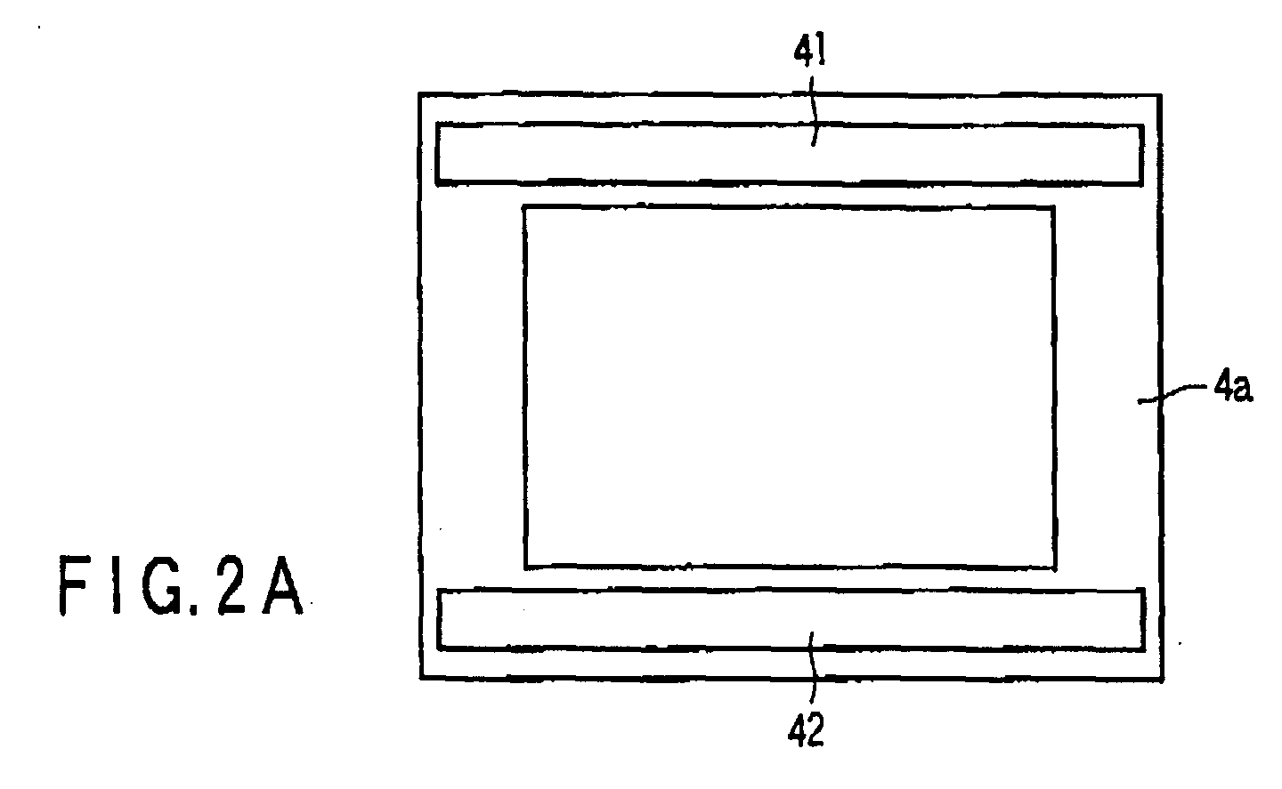
- FIGS. 2A, 2B, and 2C are respectively a plan view, a bottom view, and a side view of the loop antenna 4A.
- the loop antenna 4A has conductive patterns 41 and 42 formed on a pair of opposing pieces on the first surface (upper surface) of a double-sided printed circuit board 4a having a frame shape.
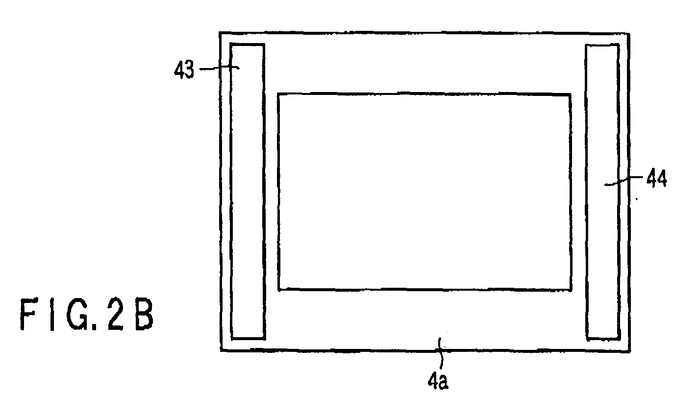
- conductive patterns 43 and 44 are formed on a pair of opposing pieces on the second surface (lower surface). The conductive patterns 41 and 42 and conductive patterns 43 and 44 form the segments of the antenna.
- the end portions of the conductive patterns 41 and 42 and conductive patterns 43 and 44 are arranged to oppose each other via the double-sided printed circuit board 4a. Accordingly, the conductive patterns 41, 42, 43, and 44 are capacitively coupled at the opposing portions, i.e., overlap portions through the dielectric of the double-sided printed circuit board 4a.
- a feed terminal is arranged at the overlap portion between the conductive patterns 42 and 44 at an arbitrary corner of the loop antenna 4A.
- the feed terminal is connected to a radio circuit 4b through a feed line pattern (not shown).
- the radio circuit 4b and the feed line pattern are mounted and formed on the printed circuit board 3b of the circuit unit 3. Accordingly, unbalanced feed is done from the radio circuit 4b to the loop antenna 4A through the feed line pattern.
- the total length of the conductive patterns 41 to 44 is set to 0.2 to 2.0 wavelength with respect to the free space wavelength of the transmission/reception frequency.
- the length of each of the conductive patterns 41 to 44 is set to be equal to or less than 0.4 wavelength with respect to the free space wavelength of the transmission/reception frequency.
- the distance between the conductive patterns at each overlap portion is set to be equal to or less than 0.1 wavelength with respect to the free space wavelength of the transmission/reception frequency.
- FIG. 3 shows the current distribution.
- the radiation pattern has a so-called doughnut shape or an almost erythrocyte (hemoglobin) shape in which a sphere is recessed at its central portion in the vertical direction with respect to the antenna surface, as shown in FIGS. 4A and 4B.
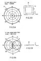
- FIGS. 5A and 5B are views showing the radiation characteristic of the radiation pattern in the horizontal plane (X-Z plane in FIGS. 5A and 5B) of the antenna.
- the radiation pattern in the horizontal plane of the antenna maintains omni-directional properties.
- FIGS. 6A and 6B show the radiation characteristic of the radiation pattern in the vertical plane (X-Y plane in FIGS. 6A and 6B) of the antenna.
- FIGS. 8A and 8B show the radiation characteristic of the radiation pattern in the vertical plane (Y-Z plane in FIGS. 8A and 8B) of the antenna.
- FIGS. 6A and 6B show the radiation characteristic of the radiation pattern in the vertical plane (X-Y plane in FIGS. 6A and 6B) of the antenna.
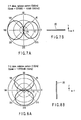
- FIGS. 6A and 6B show the characteristic when the transmission/reception frequency is 1.0 GHz. Even when the transmission/reception frequency is 0.9 GHz, a radiation pattern having a similar characteristic is obtained, as shown in FIGS. 7A and 7B.
- the distributed capacitance loop antenna 4A can generate a radiation pattern which maintains omni-directional properties in a plane parallel to the antenna surface and has a directivity with null sensitivity in a direction perpendicular to the antenna surface independently of the circumferential length of the loop.
- this loop antenna is used for a cellular phone, the influence and loss by a human body as a lossy dielectric medium are small.
- a predetermined antenna gain can be obtained independently of the tilt angle of the terminal housing during voice communication.
- the radiation resistance of the antenna can be set to a value close to the impedance (e.g., 50 ⁇ ) on the feed side of the radio circuit. For this reason, impedance matching to the radio circuit 4b can easily be ensured, as compared to a small circular loop antenna having a specific loop antenna circumferential length.
- the loop antenna 4A can be arranged around the sub-display 3c. Accordingly, the degree of freedom in mounting can be increased.
- the four conductive patterns 41 to 44 are formed as segments to form a square loop by using the both surfaces of the double-sided printed circuit board 4a having a frame shape.
- the conductive patterns 41 to 44 are capacitively coupled by making their end portions overlap via the double-sided printed circuit board 4a.
- no circuit components such as distributed capacitors need be separately prepared for capacitive coupling of the segments. Accordingly, the distributed capacitance loop antenna 4A can easily be manufactured at a low cost.
- FIG. 9 is a plan view showing a loop antenna according to the second embodiment of the present invention.
- a loop antenna 4B according to this embodiment, of four conductive patterns 45 to 48 formed on a double-sided printed circuit board 4a, the conductive patterns 45 and 46 formed on a surface which opposes a printed circuit board 3b of a circuit unit 3 shown in FIG. 1 are set to be wider than the conductive patterns 47 and 48 formed on a surface which opposes a back cover 2.
- the conductive patterns formed on the surface opposing the printed circuit board 3b of the circuit unit 3 are set to the same width as that of the conductive patterns formed on the surface opposing the back cover 2.
- near-fields generated at the overlap portions between the conductive patterns are also directed to the printed circuit board 3b of the circuit unit 3 (to the upper side in FIG. 11).
- the circuit component 3d is readily adversely affected by the near-fields. A decrease in selectivity and degradation in tuning accuracy are unavoidable.
- an adjusting structure to adjust the overlap area is formed at an end portion of a segment.
- the overlap area is arbitrarily changed in adjustment during or after the manufacture of the loop antenna.
- FIG. 12 is a view showing the first example of the loop antenna according to the third embodiment of the present invention.
- a plurality of slits 402a long in the direction of width are formed at the center of an end portion of a segment 402.
- the end portion of the segment 402 is cut at the position of an arbitrary slit 402a. Cutting can easily be done because of the presence of the slit 402a. Accordingly, the overlap area can be reduced by a simple operation.
- FIG. 13 is a view showing the second example of the loop antenna according to the third embodiment of the present invention.
- a plurality of (three in FIG. 13) comb-shaped projections 403a, 403b, and 403c are formed at an edge of a segment 403.
- an arbitrary projection e.g., the projection 403a
- Cutting can easily be done because all the projections 403a, 403b, and 403c have a long shape. Accordingly, the overlap area can be reduced by a simple operation, as in the first example.
- FIG. 14 is a view showing the third example of the loop antenna according to the third embodiment of the present invention.
- a plurality of (three in FIG. 14) comb-shaped projections 403a, 403b, and 403c are formed at the edge of the segment 403, as in the second example.
- the width of a segment 404 which overlaps the segment 403 is set to be smaller than that of the segment 403.
- the projection 403c which does not overlap the segment 404 is cut.
- a current which is normally shunted to the projection 403c flows to the remaining projections 403a and 403b. Accordingly, the density of the current flowing to the overlap portion increases. This is equivalent to an increase in overlap area.
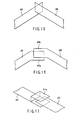
- FIG. 15 is a view showing the first example of the loop antenna according to the fourth embodiment of the present invention.
- the end portions of segments 405 and 406 are made to overlap not at a right angle but at an angle larger than 90°.
- This structure is used to form a loop antenna by, e.g., arranging a number of segments in a polygonal shape.
- FIG. 16 is a view showing the second example of the loop antenna according to the fourth embodiment of the present invention.
- This example is an improvement of the structure shown in FIG. 15.
- the end portions of segments 407 and 408 are bent in advance in accordance with the interior angle of a polygon.
- the acute-angled projecting portions of the segments 407 and 408 at the overlap portion are reduced, as compared to the example shown in FIG. 15. For this reason, a current smoothly flows, and the current distribution becomes more uniform. Accordingly, the high-frequency characteristic can be improved.
- FIG. 17 is a view showing the third example of the loop antenna according to the fourth embodiment of the present invention.
- a cantilever-shaped projecting portion 411a is formed at the end portion of one segment 411.
- the end portion of the other segment 412 is arranged and held in the gap between the end portion of the segment 411 and the projecting portion 411a. With this structure, the overlap area can be increased.
- FIG. 18 is a view showing the fourth example of the loop antenna according to the fourth embodiment of the present invention.
- This example is an improvement of the structure shown in FIG. 17.
- a cantilever-shaped projecting portion 411b at the end portion of the segment 411 is supported by two thin columns. In this structure, if the overlap area needs to be reduced, the projecting portion 411b can easily be removed.
- a loop antenna is formed by using segments having a shape except a rectangular shape.
- FIGS. 19A and 19B are views showing the first example of the loop antenna according to the fifth embodiment of the present invention.
- FIG. 19A shows one segment piece.
- FIG. 19B shows the structure of a loop antenna formed by using a plurality of (four in FIG. 19B) segment piece.
- a segment piece 421 has a shape of a combination of a plurality of triangles. When four segment pieces 421 having such a shape are arranged in a loop, a loop antenna having a square outer edge and an octagonal inner edge can be formed, as shown in FIG. 19B.
- a loop antenna in which the circumferential length changes between the outer edge and the inner edge, and the overlap amount changes between the outer periphery and the inner periphery can be formed.
- the coupling capacitance between the segment pieces can be changed, and the current distribution can arbitrarily be set.
- the current distribution on the outer periphery at the resonance frequency and that at the inner periphery at the resonance frequency can be made equal between the segment pieces.
- a loop antenna having multiple current distributions and for example, a loop antenna having a current distribution of a 1-wavelength loop antenna at the inner periphery and the current distribution of a small circular loop antenna at the outer periphery can be provided.
- the size of the hole at the central portion of the loop antenna can be adjusted in accordance with the size or shape of the circuit component arranged there. More specifically, the size of the hole at the central portion can be minimized while avoiding the circuit component. Accordingly, a broadband loop antenna can be formed while holding the degree of freedom in mounting.
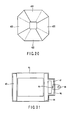
- FIG. 20 is a view showing the second example of the loop antenna according to the fifth embodiment of the present invention.
- the overlap amount on the outer periphery side is larger than that on the inner periphery side. Even in this structure, the overlap amount on the outer periphery side and that on the inner periphery side can arbitrarily be changed, as in FIGS. 19A and 19B. Accordingly, a loop antenna having an arbitrary current distribution can be implemented.
- FIG. 21 is a view showing the first example of the loop antenna according to the sixth embodiment of the present invention.
- the same reference numerals as in FIG. 2 denote the same parts in FIG. 21.
- An extended portion is formed on one side of a double-sided printed circuit board 4e.
- L-shaped matching line patterns 4f and 4g which form an impedance matching circuit are formed on the extended portion.
- the proximal portions of the matching line patterns 4f and 4g are connected to a conductive pattern 44.
- the distal end portions of the matching line patterns 4f and 4g are located to oppose each other via a slit portion 4h at a predetermined interval.
- a pair of feed terminals are formed at the distal end portions of the matching line patterns 4f and 4g.
- the feed terminals are connected to a radio circuit 4b through a feed line pattern.
- the matching line patterns 4f and 4g can be formed on the printed circuit board together with conductive patterns 41 to 44 simultaneously in one step.
- FIG. 22 is a view showing the second example of the loop antenna according to the sixth embodiment of the present invention.
- the same reference numerals as in FIG. 20 denote the same parts in FIG. 22.
- a slot 422a having a keyhole-shaped slit 422b is formed in one segment piece 422.
- a pair of feed terminals are formed at two end portions of the slit 422b.
- the feed terminals are connected to the radio circuit 4b through a feed line pattern.
- FIG. 23 is a view showing the third example of the loop antenna according to the sixth embodiment of the present invention.
- a slot 423c for impedance matching' is formed in each of four segment pieces 423.
- one of the slots 423c has a slit 423b similar to that shown in FIG. 22.
- a pair of feed terminals are formed at two end portions of the slit 422b. The feed terminals are connected to the radio circuit 4b through a feed line pattern.
- FIG. 24 is a view showing the fourth example of the loop antenna according to the sixth embodiment of the present invention.
- one segment piece 431 in a loop antenna formed by arranging four segment pieces 431 to 434 in a square, one segment piece 431 has a U shape, and a pair of feed terminals are formed at two end portions of the segment piece 431.
- the feed terminals are connected to the radio circuit 4b through a feed line pattern.
- impedance matching to the radio circuit 4b can be set high. Accordingly, impedance matching can be ensured without separately preparing a matching circuit.
- FIG. 25 is a view showing the fifth example of the loop antenna according to the sixth embodiment of the present invention.
- FIG. 25 is an enlarged view of the U-shaped segment piece 431 shown in FIG. 24.
- a U-shaped slot 441a is formed n a U-shaped segment piece 441.
- a slit 441b is formed at the central portion between segment piece peripheral portions 441c and 441d which are left after formation of the slot 441a.
- a pair of feed terminals are formed at two end portions of the slit 441b. The feed terminals are connected to the radio circuit 4b through a feed line pattern.
- impedance matching to the radio circuit 4b can be set higher. Accordingly, impedance matching can be ensured without separately preparing a matching circuit.
- FIG. 26 is a view showing the sixth example of the loop antenna according to the sixth embodiment of the present invention.
- a pair of crank-shaped matching lines 4i and 4j stand on the center line in the longitudinal direction of a conductive pattern 43.
- the proximal portions of the matching lines 4i and 4j are electrically connected to the conductive pattern 43.
- the distal end pieces of the matching lines 4i and 4j are located to oppose each other at a predetermined interval.
- a pair of feed terminals are formed at the distal end pieces of the matching lines 4i and 4j.
- the feed terminals are connected to the radio circuit 4b through a feed line pattern.
- the current which flows to the closed loop of the matching circuit is larger than the current which flows to the closed loop of the main antenna.
- a radiation pattern is formed in a direction perpendicular to the loop antenna plane by the closed loop current in the matching circuit. This radiation pattern may influence the human body and degrade the tuning accuracy in the free space.
- an overlap structure is implemented by using a double-sided printed circuit board.
- the present invention is not limited to this.
- An overlap structure may be implemented on a single-sided printed circuit board.
- FIG. 27 shows an example of the structure.
- Four L-shaped conductive patterns 451 to 454 are arranged in a square to form a loop on a single-sided printed circuit board 4k.
- One end portion of each of the conductive patterns 451 to 454 is located to oppose the other end portion of an adjacent conductive pattern at a predetermined interval.
- the coupling capacitance between the conductive patterns 451 to 454 is determined by the interval and the length of the opposite portions.
- a C-shaped conductive pattern 46 is formed at a position opposite to the conductive pattern 454 while being separated by a predetermined distance. Two end portions of the conductive pattern 46 are connected to a radio circuit 4b.
- the overlap structure using the single-sided printed circuit board does not require mounting of a delicate circuit component, like the above-described overlap structure using a double-sided printed circuit board, and can therefore be made thin like a sheet.
- soldering is unnecessary, manufacture is easy, and a flexible loop antenna using a flexible board can be manufactured.
- loop antennas using a printed circuit board have been described.
- a loop antenna may be manufactured by using, e.g., a laminate coating or resin integral molding (MID) instead of using a printed circuit board.
- MID resin integral molding
- As a feed method not unbalanced feed but balanced feed which executes power supply between segments and a ground terminal may be employed.
Landscapes
- Engineering & Computer Science (AREA)
- Computer Networks & Wireless Communication (AREA)
- Support Of Aerials (AREA)
- Details Of Aerials (AREA)
- Transceivers (AREA)
- Telephone Set Structure (AREA)
Abstract
Description
- The present invention relates to a loop antenna suitable for a mobile communication terminal such as a cellular phone or PDA (Personal Digital Assistants) and a radio communication device having the loop antenna.
- Recent mobile communication terminals such as cellular phones and PDAs use internal antennas having an antenna element accommodated in a housing from the viewpoint of further size reduction and design of terminals. However, an internal antenna readily degrades its performance in the voice communication posture, as compared to an antenna arranged outside the housing.
- The antenna performance can deteriorate in the voice communication posture due to two reasons below.
- (1) During voice communication, the terminal housing readily comes close to the speaker as a lossy dielectric medium. Since the transmission radio wave absorption amount in the lossy dielectric medium increases, the radiation efficiency decreases.
- (2) During voice communication, the terminal housing is often tilted obliquely or horizontally. For this reason, the reception efficiency for a vertical polarized wave arriving from the base station decreases.
-
- In addition, the antenna radiation pattern changes depending on the tilt angle of the terminal housing in the voice communication posture. This also poses a problem in maintaining a stable voice communication state.
- So use of a traditional small circular loop antenna could be preliminary approach to examine. A small circular loop antenna is formed by a 0.1-wavelength antenna segment having a ring shape. With this antenna, a radiation pattern with radiation suppressed in a direction toward the speaker can be obtained. In addition, a predetermined antenna gain can be held independently of the tilt angle of the terminal housing during voice communication. However, since the small circular loop antenna has a short circumferential length, the radiation resistance is low, and the aperture area is small. For this reason, impedance matching to a radio circuit is difficult to ensure.
- On the other hand, as an internal antenna of another type suitable for mobile communication terminals, a dipole antenna which has a Z- or H-shaped segment and supplies power at the central segment portion has been proposed in, e.g., U.S. Patent No. 5,767,809 or Chi-Chang, et al, "A 2.4 GHz Omni-directional Horizontally Polarized Planar Printed Antenna for WLAN Applications", 2003 IEEE. An antenna of this type can obtain a radiation pattern similar to that of a small circular loop antenna. In addition, impedance matching to a radio circuit can easily be ensured.
- However, an antenna of this type has a segment at the antenna central portion and supplies power on the central segment. It is therefore difficult to use this antenna in a radio communication device having a large circuit component mounted at the central portion of the housing, like a folding cellular phone having a back display.
- As described above, the conventionally developed or proposed internal antennas can hardly obtain impedance matching to a radio circuit because of their low radiation resistance and small aperture area. In addition, since a central segment and power supply at the central portion of the segment are necessary, the degree of freedom in mounting is low. For this reason, the antennas are not appropriate for compact radio communication devices having many restrictions on mounting, like a cellular phone having a back display.
- It is an object of the present invention to provide a loop antenna which can obtain an ideal radiation pattern and also easily obtain impedance matching to a radio circuit and increases the degree of freedom in mounting by eliminating the necessity of the central segment and power supply at its central portion, and a radio communication device having the loop antenna.
- In order to achieve the above object, according to one aspect of the present invention, in a loop antenna, a plurality of segments are arranged in a loop, the segments are capacitively coupled, and a feed circuit is connected to least one of the plurality of segments.
- This summary of the invention does not necessarily describe all necessary features so that the invention may also be a sub-combination of these described features.
- The invention can be more fully understood from the following detailed description when taken in conjunction with the accompanying drawings, in which:
- FIG. 1 is an exploded perspective view showing a radio communication device having a loop antenna according to the first embodiment of the present invention;
- FIGS. 2A, 2B, and 2C are enlarged views showing the structure of the loop antenna shown in FIG. 1;
- FIG. 3 is a view showing a current distribution in the loop antenna shown in FIG. 1;
- FIGS. 4A and 4B are views showing a three-dimensional expression of the radiation pattern by the loop antenna shown in FIG. 1;
- FIGS. 5A and 5B are views showing the radiation pattern in the X-Z plane of the loop antenna shown in FIG. 1;
- FIGS. 6A and 6B are views showing the radiation pattern at 1.0 GHz in the X-Y plane of the loop antenna shown in FIG. 1;
- FIGS. 7A and 7B are views showing the radiation pattern at 0.9 GHz in the X-Y plane of the loop antenna shown in FIG. 1;
- FIGS. 8A and 8B are views showing the radiation pattern in the Y-Z plane of the loop antenna shown in FIG. 1;
- FIG. 9 is a plan view showing a loop antenna according to the second embodiment of the present invention;
- FIG. 10 is a view showing a near-field generation state at the overlap portion of the loop antenna shown in FIG. 9;
- FIG. 11 is a view showing a near-field generation state at the overlap portion of the loop antenna in which the conductive patterns are set to the same width;
- FIG. 12 is a view showing the first example of a loop antenna according to the third embodiment of the present invention;
- FIG. 13 is a view showing the second example of the loop antenna according to the third embodiment of the present invention;
- FIG. 14 is a view showing the third example of the loop antenna according to the third embodiment of the present invention;
- FIG. 15 is a view showing the first example of a loop antenna according to the fourth embodiment of the present invention;
- FIG. 16 is a view showing the second example of the loop antenna according to the fourth embodiment of the present invention;
- FIG. 17 is a view showing the third example of the loop antenna according to the fourth embodiment of the present invention;
- FIG. 18 is a view showing the fourth example of the loop antenna according to the fourth embodiment of the present invention;
- FIGS. 19A and 19B are views showing the first example of a loop antenna according to the fifth embodiment of the present invention;
- FIG. 20 is a view showing the second example of the loop antenna according to the fifth embodiment of the present invention;
- FIG. 21 is a view showing the first example of a loop antenna according to the sixth embodiment of the present invention;
- FIG. 22 is a view showing the second example of the loop antenna according to the sixth embodiment of the present invention;
- FIG. 23 is a view showing the third example of the loop antenna according to the sixth embodiment of the present invention;
- FIG. 24 is a view showing the fourth example of the loop antenna according to the sixth embodiment of the present invention;
- FIG. 25 is a view showing the fifth example of the loop antenna according to the sixth embodiment of the present invention;
- FIG. 26 is a view showing the sixth example of the loop antenna according to the sixth embodiment of the present invention; and
- FIG. 27 is a plan view showing the structure of a loop antenna according to other embodiments of the present invention.
-
- FIG. 1 is an exploded perspective view showing a radio communication device having a loop antenna according to the first embodiment of the present invention. The radio communication device of the first embodiment is a folding cellular phone. FIG. 1 shows only the upper structure. The lower structure in which a keypad and the like are arranged is not illustrated.
- Referring to FIG. 1,
reference numeral 1 denotes a front cover. Adisplay window 1a for main display is arranged in the front cover.Reference numeral 2 in FIG. 1 denotes a back cover. Adisplay window 2a for sub-display is arranged on theback cover 2. Thefront cover 1 andback cover 2 form an upper housing. Acircuit unit 3 is accommodated in the upper housing. In thecircuit unit 3, a main display (not shown), a printedcircuit board 3b to which circuit elements are attached, and a sub-display 3c are mounted in acase 3a. - A
loop antenna 4A is arranged on the printedcircuit board 3b of thecircuit unit 3 and surrounds the sub-display 3c. FIGS. 2A, 2B, and 2C are respectively a plan view, a bottom view, and a side view of theloop antenna 4A. - As shown in FIGS. 2A, 2B, and 2C, the
loop antenna 4A hasconductive patterns circuit board 4a having a frame shape. In addition,conductive patterns conductive patterns conductive patterns - The end portions of the
conductive patterns conductive patterns circuit board 4a. Accordingly, theconductive patterns circuit board 4a. - A feed terminal is arranged at the overlap portion between the
conductive patterns loop antenna 4A. The feed terminal is connected to aradio circuit 4b through a feed line pattern (not shown). Theradio circuit 4b and the feed line pattern are mounted and formed on the printedcircuit board 3b of thecircuit unit 3. Accordingly, unbalanced feed is done from theradio circuit 4b to theloop antenna 4A through the feed line pattern. - The total length of the
conductive patterns 41 to 44 is set to 0.2 to 2.0 wavelength with respect to the free space wavelength of the transmission/reception frequency. The length of each of theconductive patterns 41 to 44 is set to be equal to or less than 0.4 wavelength with respect to the free space wavelength of the transmission/reception frequency. The distance between the conductive patterns at each overlap portion is set to be equal to or less than 0.1 wavelength with respect to the free space wavelength of the transmission/reception frequency. - In the above-described structure, when a power is supplied to the
loop antenna 4A, in-phase currents flow to theconductive patterns 41 to 44 which form the segments because they are capacitively coupled with each other. FIG. 3 shows the current distribution. The radiation pattern has a so-called doughnut shape or an almost erythrocyte (hemoglobin) shape in which a sphere is recessed at its central portion in the vertical direction with respect to the antenna surface, as shown in FIGS. 4A and 4B. - FIGS. 5A and 5B are views showing the radiation characteristic of the radiation pattern in the horizontal plane (X-Z plane in FIGS. 5A and 5B) of the antenna. As is apparent from FIGS. 5A and 5B, the radiation pattern in the horizontal plane of the antenna maintains omni-directional properties. FIGS. 6A and 6B show the radiation characteristic of the radiation pattern in the vertical plane (X-Y plane in FIGS. 6A and 6B) of the antenna. FIGS. 8A and 8B show the radiation characteristic of the radiation pattern in the vertical plane (Y-Z plane in FIGS. 8A and 8B) of the antenna. As is apparent from FIGS. 6A, 6B, 8A, and 8B, the radiation pattern in the vertical plane of the antenna obtains only a directivity in the horizontal directions X and Z. No radiation occurs along the vertical direction Y. FIGS. 6A and 6B show the characteristic when the transmission/reception frequency is 1.0 GHz. Even when the transmission/reception frequency is 0.9 GHz, a radiation pattern having a similar characteristic is obtained, as shown in FIGS. 7A and 7B.
- That is, the distributed
capacitance loop antenna 4A according to the first embodiment can generate a radiation pattern which maintains omni-directional properties in a plane parallel to the antenna surface and has a directivity with null sensitivity in a direction perpendicular to the antenna surface independently of the circumferential length of the loop. When this loop antenna is used for a cellular phone, the influence and loss by a human body as a lossy dielectric medium are small. In addition, a predetermined antenna gain can be obtained independently of the tilt angle of the terminal housing during voice communication. - Since the circumferential length of the loop antenna can arbitrarily be set, the radiation resistance of the antenna can be set to a value close to the impedance (e.g., 50 Ω) on the feed side of the radio circuit. For this reason, impedance matching to the
radio circuit 4b can easily be ensured, as compared to a small circular loop antenna having a specific loop antenna circumferential length. - In addition, neither central segment nor power supply on the central segment are necessary, unlike the Z- or H-shaped antenna. Hence, even in the folding cellular phone having the sub-display 3c on the rear surface, as shown in FIG. 1, the
loop antenna 4A can be arranged around the sub-display 3c. Accordingly, the degree of freedom in mounting can be increased. - In addition, in this embodiment, the four
conductive patterns 41 to 44 are formed as segments to form a square loop by using the both surfaces of the double-sided printedcircuit board 4a having a frame shape. Theconductive patterns 41 to 44 are capacitively coupled by making their end portions overlap via the double-sided printedcircuit board 4a. Hence, no circuit components such as distributed capacitors need be separately prepared for capacitive coupling of the segments. Accordingly, the distributedcapacitance loop antenna 4A can easily be manufactured at a low cost. - FIG. 9 is a plan view showing a loop antenna according to the second embodiment of the present invention. In a loop antenna 4B according to this embodiment, of four
conductive patterns 45 to 48 formed on a double-sided printedcircuit board 4a, theconductive patterns circuit board 3b of acircuit unit 3 shown in FIG. 1 are set to be wider than theconductive patterns back cover 2. - In this structure, as shown in FIG. 10, near-fields generated at the overlap portions between the
conductive patterns conductive patterns back cover 2 shown in FIG. 1 (to the lower side in FIG. 10) and are hardly directed to the printedcircuit board 3b of the circuit unit 3 (to the upper side in FIG. 10). Even when acircuit component 3d is present between the loop antenna 4B and the printedcircuit board 3b of thecircuit unit 3, the adverse affect of the near-field on thecircuit component 3d is reduced. As a result, any decrease in selectivity and degradation in tuning accuracy are prevented. - Assume that the conductive patterns formed on the surface opposing the printed
circuit board 3b of thecircuit unit 3 are set to the same width as that of the conductive patterns formed on the surface opposing theback cover 2. In this case, as shown in FIG. 11, near-fields generated at the overlap portions between the conductive patterns are also directed to the printedcircuit board 3b of the circuit unit 3 (to the upper side in FIG. 11). For this reason, thecircuit component 3d is readily adversely affected by the near-fields. A decrease in selectivity and degradation in tuning accuracy are unavoidable. - In the third embodiment of the present invention, an adjusting structure to adjust the overlap area is formed at an end portion of a segment. By using the adjusting structure, the overlap area is arbitrarily changed in adjustment during or after the manufacture of the loop antenna.
- FIG. 12 is a view showing the first example of the loop antenna according to the third embodiment of the present invention. A plurality of
slits 402a long in the direction of width are formed at the center of an end portion of asegment 402. To adjust the overlap area between asegment 401 and thesegment 402, the end portion of thesegment 402 is cut at the position of anarbitrary slit 402a. Cutting can easily be done because of the presence of theslit 402a. Accordingly, the overlap area can be reduced by a simple operation. - FIG. 13 is a view showing the second example of the loop antenna according to the third embodiment of the present invention. A plurality of (three in FIG. 13) comb-shaped
projections segment 403. To adjust the overlap area between thesegment 401 and thesegment 403, an arbitrary projection (e.g., theprojection 403a) is cut at its base. Cutting can easily be done because all theprojections - FIG. 14 is a view showing the third example of the loop antenna according to the third embodiment of the present invention. A plurality of (three in FIG. 14) comb-shaped
projections segment 403, as in the second example. On the other hand, the width of asegment 404 which overlaps thesegment 403 is set to be smaller than that of thesegment 403. - In this structure, to adjust the overlap area between the
segment 403 and thesegment 404, of theprojections segment 403, theprojection 403c which does not overlap thesegment 404 is cut. In this case, a current which is normally shunted to theprojection 403c flows to the remainingprojections - In the fourth embodiment of the loop antenna according to the present invention, various kinds of overlap structures will be described.
- FIG. 15 is a view showing the first example of the loop antenna according to the fourth embodiment of the present invention. In this example, the end portions of
segments - FIG. 16 is a view showing the second example of the loop antenna according to the fourth embodiment of the present invention. This example is an improvement of the structure shown in FIG. 15. The end portions of
segments segments - FIG. 17 is a view showing the third example of the loop antenna according to the fourth embodiment of the present invention. In this example, a cantilever-shaped projecting portion 411a is formed at the end portion of one
segment 411. The end portion of theother segment 412 is arranged and held in the gap between the end portion of thesegment 411 and the projecting portion 411a. With this structure, the overlap area can be increased. - FIG. 18 is a view showing the fourth example of the loop antenna according to the fourth embodiment of the present invention. This example is an improvement of the structure shown in FIG. 17. A cantilever-shaped projecting
portion 411b at the end portion of thesegment 411 is supported by two thin columns. In this structure, if the overlap area needs to be reduced, the projectingportion 411b can easily be removed. - In the fifth embodiment of a loop antenna according to the present invention, a loop antenna is formed by using segments having a shape except a rectangular shape.
- FIGS. 19A and 19B are views showing the first example of the loop antenna according to the fifth embodiment of the present invention. FIG. 19A shows one segment piece. FIG. 19B shows the structure of a loop antenna formed by using a plurality of (four in FIG. 19B) segment piece. A
segment piece 421 has a shape of a combination of a plurality of triangles. When foursegment pieces 421 having such a shape are arranged in a loop, a loop antenna having a square outer edge and an octagonal inner edge can be formed, as shown in FIG. 19B. - With this structure, a loop antenna in which the circumferential length changes between the outer edge and the inner edge, and the overlap amount changes between the outer periphery and the inner periphery can be formed. When the overlap amount on the outer periphery side and that on the inner periphery side are arbitrarily changed, the coupling capacitance between the segment pieces can be changed, and the current distribution can arbitrarily be set. For example, the current distribution on the outer periphery at the resonance frequency and that at the inner periphery at the resonance frequency can be made equal between the segment pieces. In addition, a loop antenna having multiple current distributions, and for example, a loop antenna having a current distribution of a 1-wavelength loop antenna at the inner periphery and the current distribution of a small circular loop antenna at the outer periphery can be provided.
- Furthermore, the size of the hole at the central portion of the loop antenna can be adjusted in accordance with the size or shape of the circuit component arranged there. More specifically, the size of the hole at the central portion can be minimized while avoiding the circuit component. Accordingly, a broadband loop antenna can be formed while holding the degree of freedom in mounting.
- FIG. 20 is a view showing the second example of the loop antenna according to the fifth embodiment of the present invention. In the loop antenna of this example, the overlap amount on the outer periphery side is larger than that on the inner periphery side. Even in this structure, the overlap amount on the outer periphery side and that on the inner periphery side can arbitrarily be changed, as in FIGS. 19A and 19B. Accordingly, a loop antenna having an arbitrary current distribution can be implemented.
- In the sixth embodiment of the present invention, various kinds of feed circuits suitable for the loop antenna of the present invention will be described.
- FIG. 21 is a view showing the first example of the loop antenna according to the sixth embodiment of the present invention. The same reference numerals as in FIG. 2 denote the same parts in FIG. 21.
- An extended portion is formed on one side of a double-sided printed
circuit board 4e. L-shapedmatching line patterns matching line patterns conductive pattern 44. The distal end portions of thematching line patterns slit portion 4h at a predetermined interval. A pair of feed terminals are formed at the distal end portions of thematching line patterns radio circuit 4b through a feed line pattern. - With this structure, impedance matching to the
radio circuit 4b can more accurately be ensured. In addition, thematching line patterns conductive patterns 41 to 44 simultaneously in one step. - FIG. 22 is a view showing the second example of the loop antenna according to the sixth embodiment of the present invention. The same reference numerals as in FIG. 20 denote the same parts in FIG. 22. A
slot 422a having a keyhole-shapedslit 422b is formed in onesegment piece 422. A pair of feed terminals are formed at two end portions of theslit 422b. The feed terminals are connected to theradio circuit 4b through a feed line pattern. With this structure, even in the loop antenna whose circumferential length changes between the outer edge and the inner edge, impedance matching to theradio circuit 4b can more reliably be ensured. - FIG. 23 is a view showing the third example of the loop antenna according to the sixth embodiment of the present invention. A
slot 423c for impedance matching'is formed in each of foursegment pieces 423. one of theslots 423c has aslit 423b similar to that shown in FIG. 22. A pair of feed terminals are formed at two end portions of theslit 422b. The feed terminals are connected to theradio circuit 4b through a feed line pattern. With this structure, in the loop antenna whose overlap amount changes between the outer periphery side and the inner periphery side, optimum impedance matching can be ensured for eachsegment piece 423. - FIG. 24 is a view showing the fourth example of the loop antenna according to the sixth embodiment of the present invention. In this example, in a loop antenna formed by arranging four
segment pieces 431 to 434 in a square, onesegment piece 431 has a U shape, and a pair of feed terminals are formed at two end portions of thesegment piece 431. The feed terminals are connected to theradio circuit 4b through a feed line pattern. With this structure, impedance matching to theradio circuit 4b can be set high. Accordingly, impedance matching can be ensured without separately preparing a matching circuit. - FIG. 25 is a view showing the fifth example of the loop antenna according to the sixth embodiment of the present invention. FIG. 25 is an enlarged view of the
U-shaped segment piece 431 shown in FIG. 24. In this example, aU-shaped slot 441a is formed n aU-shaped segment piece 441. Aslit 441b is formed at the central portion between segment pieceperipheral portions slot 441a. A pair of feed terminals are formed at two end portions of theslit 441b. The feed terminals are connected to theradio circuit 4b through a feed line pattern. - With this structure, impedance matching to the
radio circuit 4b can be set higher. Accordingly, impedance matching can be ensured without separately preparing a matching circuit. - FIG. 26 is a view showing the sixth example of the loop antenna according to the sixth embodiment of the present invention. A pair of crank-shaped
matching lines 4i and 4j stand on the center line in the longitudinal direction of aconductive pattern 43. The proximal portions of thematching lines 4i and 4j are electrically connected to theconductive pattern 43. The distal end pieces of thematching lines 4i and 4j are located to oppose each other at a predetermined interval. A pair of feed terminals are formed at the distal end pieces of thematching lines 4i and 4j. The feed terminals are connected to theradio circuit 4b through a feed line pattern. - With this structure, impedance matching to the
radio circuit 4b can accurately be ensured, as a matter of course. Additionally, generation of a radiation pattern in a direction perpendicular to the loop antenna plane by thematching lines 4i and 4j can be reduced. Accordingly, the influence of the radio wave on a human body can be reduced. - When the matching circuit is present in the same plane as the main loop of the antenna, as shown in FIG. 26, the current which flows to the closed loop of the matching circuit is larger than the current which flows to the closed loop of the main antenna. In this case, a radiation pattern is formed in a direction perpendicular to the loop antenna plane by the closed loop current in the matching circuit. This radiation pattern may influence the human body and degrade the tuning accuracy in the free space.
- When the
matching lines 4i and 4j are formed along the center line of the conductive pattern, as shown in FIG. 26, formation of the radiation pattern in a direction perpendicular to the loop antenna plane by the closed loop current in the matching circuit can be prevented. Hence, influence of the radiation pattern on the human body can be suppressed, and the tuning accuracy in the free space can be held high. - In the above-described embodiments, an overlap structure is implemented by using a double-sided printed circuit board. However, the present invention is not limited to this. An overlap structure may be implemented on a single-sided printed circuit board.
- FIG. 27 shows an example of the structure. Four L-shaped
conductive patterns 451 to 454 are arranged in a square to form a loop on a single-sided printedcircuit board 4k. One end portion of each of theconductive patterns 451 to 454 is located to oppose the other end portion of an adjacent conductive pattern at a predetermined interval. The coupling capacitance between theconductive patterns 451 to 454 is determined by the interval and the length of the opposite portions. A C-shapedconductive pattern 46 is formed at a position opposite to theconductive pattern 454 while being separated by a predetermined distance. Two end portions of theconductive pattern 46 are connected to aradio circuit 4b. - With this structure, an in-plane overlap structure and a noncontact feed circuit are implemented. The overlap structure using the single-sided printed circuit board does not require mounting of a delicate circuit component, like the above-described overlap structure using a double-sided printed circuit board, and can therefore be made thin like a sheet. In addition, since soldering is unnecessary, manufacture is easy, and a flexible loop antenna using a flexible board can be manufactured.
- In the above-described embodiments, loop antennas using a printed circuit board have been described. However, the present invention is not limited to this. A loop antenna may be manufactured by using, e.g., a laminate coating or resin integral molding (MID) instead of using a printed circuit board. As a feed method, not unbalanced feed but balanced feed which executes power supply between segments and a ground terminal may be employed.
- For the shapes and number of segments, the structure of the capacitive coupling portion, and the structure of the feed circuit, various changes and modifications can be made as well without departing from the spirit and scope of the present invention.
- The present invention is not limited to the above-described embodiments, and in practicing the present invention, various changes and modifications can be made for the constituent elements without departing from the spirit and scope of the invention. In addition, various inventions can be implemented by appropriately combining a plurality of constituent elements disclosed in the embodiments. For example, some of constituent elements disclosed in the embodiments may be omitted. Alternatively, constituent elements in different embodiments may be combined.
Claims (18)
- A loop antenna characterized by comprising:a plurality of segments (41, 42, 43, 44) which are arranged in a loop;a coupling medium (4a) which capacitively couples the plurality of segments (41, 42, 43, 44); anda circuit to connect a feed circuit (4b) to at least one of the plurality of segments (41, 42, 43, 44).
- A loop antenna characterized by comprising:a plurality of segments (41, 42, 43, 44) which are arranged in a loop while overlapping each other at end portions;a dielectric medium (4a) which is inserted between overlap portions of the plurality of segments (41, 42, 43, 44) to capacitively couple the plurality of segments (41, 42, 43, 44); anda circuit to connect a feed circuit (4b) to at least one of the plurality of segments (41, 42, 43, 44).
- The antenna according to claim 2, characterized in that the plurality of segments include a plurality of plate-shaped pieces of conductors (421), the conductors (421) being arranged to form a polygon while overlapping each other at end portions.
- The antenna according to claim 2, characterized in that the plurality of segments include a plurality of conductive patterns (41, 42, 43, 44) distributed to a first surface and a second surface of a double-sided printed circuit board (4a), the plurality of conductive patterns (41, 42, 43, 44) having overlap portions at which end portions oppose each other via the double-sided printed circuit board (4a), and
the dielectric medium includes the double-sided printed circuit board (4a) which is inserted between the overlap portions of the plurality of conductive patterns (41, 42, 43, 44). - The antenna according to claim 2, characterized in that the plurality of segments include a plurality of conductive patterns (451, 452, 453, 454) arranged in a loop on the same plane of a printed circuit board (4k), the plurality of conductive patterns (451, 452, 453, 454) having overlap portions which oppose each other at a predetermined interval in a direction parallel to a surface of the printed circuit board (4k), and
the dielectric medium includes the printed circuit board (4k) and air layers which are present at the overlap portions of the plurality of conductive patterns (451, 452, 453, 454). - The antenna according to claim 2, characterized in that in the plurality of segments, one segment (47, 48) is formed to be narrower than the other segment (45, 46) at least at each overlap portion.
- The antenna according to claim 2, characterized in that the plurality of segments include an area adjusting structure (402a, 403a, 403b, 403c) to adjust an overlap area at each overlap portion.
- The antenna according to claim 2, characterized in that the circuit to connect the feed circuit (4b) comprises
a pair of L-shaped matching lines (4f, 4g) which have proximal portions connected to the segment (44) and distal end portions separated by a predetermined interval (4h), and
a feed line which connects the feed circuit (4b) between the distal end portions of the pair of matching lines (4f, 4g). - The antenna according to claim 2, characterized in that the circuit to connect the feed circuit (4b) comprises
a pair of crank-shaped matching lines (41, 4j) which stand in a direction perpendicular to the segment (43) and have proximal portions connected to the segment (43) and distal end portions separated by a predetermined interval, and
a feed line which connects the feed circuit (4b) between the distal end portions of the pair of matching lines (4i, 4j). - A radio communication device characterized by comprising:a housing (1, 2);a printed circuit board (3b) which is accommodated in the housing (1, 2);a circuit component (3c) which is mounted on the printed circuit board (3b); anda loop antenna (4A) which is arranged in the housing (1, 2) while overlapping the printed circuit board (3b),the loop antenna (4A) comprisinga plurality of segments (41, 42, 43, 44) which are arranged in a loop around the circuit component (3c),a capacitive coupling medium (4a) which capacitively couples the plurality of segments (41, 42, 43, 44), anda circuit which connects a feed circuit (4b) to at least one of the plurality of segments (41, 42, 43, 44).
- A radio communication device characterized by comprising:a housing (1, 2);a printed circuit board (3b) which is accommodated in the housing (1, 2);a circuit component (3c) which is mounted on the printed circuit board (3b); anda loop antenna (4A) which is arranged in the housing (1, 2) while overlapping the printed circuit board (3b),the loop antenna (4A) comprisinga plurality of segments (41, 42, 43, 44) which are arranged in a loop around the circuit component (3b) while overlapping each other at end portions;a dielectric medium (4a) which is inserted between overlap portions of the plurality of segments (41, 42, 43, 44) to capacitively couple the plurality of segments (41, 42, 43, 44); anda circuit to connect a feed circuit (4b) to at least one of the plurality of segments (41, 42, 43, 44).
- The device according to claim 11, characterized in that the plurality of segments include four plate-shaped conductors (41, 42, 43, 44), the plate-shaped conductors (41, 42, 43, 44) being arranged to form a square around the circuit component (3c) while overlapping each other at end portions.
- The device according to claim 11, characterized in that the plurality of segments include a plurality of conductive patterns (41, 42, 43, 44) distributed to a first surface and a second surface of a ring-shaped double-sided printed circuit board (4a), the plurality of conductive patterns (41, 42, 43, 44) having overlap portions at which end portions oppose each other via the double-sided printed circuit board (4a), and
the dielectric medium includes the double-sided printed circuit board (4a) which is inserted between the overlap portions of the plurality of conductive patterns (41, 42, 43, 44). - The device according to claim 11, characterized in that in the plurality of segments, one segment (47, 48) is set to be narrower than the other segment (45, 46) at least at each overlap portion.
- A device according to claim 14, characterized in that in the plurality of segments, a segment (45) arranged closer to the circuit component (3d) is set to be wider than a segment (47) arranged far from the circuit component (3d).
- The device according to claim 11, characterized in that the plurality of segments include an area adjusting structure (402a, 403a, 403b, 403c) to adjust an overlap area at each overlap portion.
- The device according to claim 11, characterized in that the circuit to connect the feed circuit (4b) comprises
a pair of L-shaped matching lines (4f, 4g) which have proximal portions connected to the segment (44) and distal end portions separated by a predetermined interval (4h), and
a feed line which connects the feed circuit (4b) between the distal end portions of the pair of matching lines (4f, 4g). - The device according to claim 11, characterized in that the circuit to connect the feed circuit (4b) comprises
a pair of crank-shaped matching lines (4i, 4j) which stand in a direction perpendicular to the segment (43) and have proximal portions connected to the segment (43) and distal end portions separated by a predetermined interval, and
a feed line which connects the feed circuit (4b) between the distal end portions of the pair of matching lines (4i, 4j).
Applications Claiming Priority (2)
| Application Number | Priority Date | Filing Date | Title |
|---|---|---|---|
| JP2004005438 | 2004-01-13 | ||
| JP2004005438A JP3790249B2 (en) | 2004-01-13 | 2004-01-13 | Loop antenna and wireless communication device equipped with loop antenna |
Publications (1)
| Publication Number | Publication Date |
|---|---|
| EP1555714A1 true EP1555714A1 (en) | 2005-07-20 |
Family
ID=34616837
Family Applications (1)
| Application Number | Title | Priority Date | Filing Date |
|---|---|---|---|
| EP04022796A Withdrawn EP1555714A1 (en) | 2004-01-13 | 2004-09-24 | Loop antenna and radio communication device having the same |
Country Status (4)
| Country | Link |
|---|---|
| US (1) | US7113143B2 (en) |
| EP (1) | EP1555714A1 (en) |
| JP (1) | JP3790249B2 (en) |
| CN (1) | CN1655398A (en) |
Cited By (6)
| Publication number | Priority date | Publication date | Assignee | Title |
|---|---|---|---|---|
| WO2006109184A1 (en) * | 2005-04-15 | 2006-10-19 | Nokia Corporation | An antenna having a plurality of resonant frequencies |
| WO2007084510A1 (en) * | 2006-01-18 | 2007-07-26 | Impinj, Inc. | Discontinuous-loop rfid reader antenna and methods |
| USD570337S1 (en) | 2006-08-25 | 2008-06-03 | Impinj, Inc. | Broken-loop RFID reader antenna for near field and far field UHF RFID tags |
| EP1935055A4 (en) * | 2005-09-15 | 2009-05-27 | Motorola Inc | Wireless communication device with integrated antenna |
| WO2010144886A1 (en) * | 2009-06-12 | 2010-12-16 | Qualcomm Incorporated | Devices and methods related to a display assembly including an antenna |
| JP2015525048A (en) * | 2012-08-20 | 2015-08-27 | ノキア コーポレイション | Antenna device and manufacturing method thereof |
Families Citing this family (24)
| Publication number | Priority date | Publication date | Assignee | Title |
|---|---|---|---|---|
| JP3791923B2 (en) * | 2004-01-13 | 2006-06-28 | 株式会社東芝 | Wireless communication terminal |
| JP4955966B2 (en) * | 2005-09-05 | 2012-06-20 | キヤノン株式会社 | Waveguide, device using the same, and detection method |
| US7773041B2 (en) * | 2006-07-12 | 2010-08-10 | Apple Inc. | Antenna system |
| JP5114045B2 (en) * | 2006-11-27 | 2013-01-09 | 日本電気株式会社 | Antenna device and portable radio terminal |
| KR20080061274A (en) * | 2006-12-27 | 2008-07-02 | 가부시키가이샤 한도오따이 에네루기 켄큐쇼 | Antenna and semiconductor device having the antenna |
| US7830311B2 (en) * | 2007-07-18 | 2010-11-09 | Murata Manufacturing Co., Ltd. | Wireless IC device and electronic device |
| US8866616B2 (en) * | 2007-08-22 | 2014-10-21 | Tyco Fire & Security Gmbh | RFID tag having antenna with co-planar radiation pattern |
| US7847697B2 (en) * | 2008-02-14 | 2010-12-07 | 3M Innovative Properties Company | Radio frequency identification (RFID) tag including a three-dimensional loop antenna |
| US20110128199A1 (en) * | 2009-10-29 | 2011-06-02 | Ziming He | Field-confined wideband antenna for radio frequency front end integrated circuits |
| JP2011139283A (en) * | 2009-12-28 | 2011-07-14 | Sony Corp | Electronic apparatus, and communication device |
| TWI508367B (en) * | 2012-09-27 | 2015-11-11 | Ind Tech Res Inst | Communication device and method for designing antenna element thereof |
| WO2014146715A1 (en) * | 2013-03-21 | 2014-09-25 | Telefonaktiebolaget L M Ericsson (Publ) | An active antenna |
| JP2015070478A (en) * | 2013-09-30 | 2015-04-13 | 東京コスモス電機株式会社 | Electrostatic coupling antenna |
| CN106033988A (en) * | 2015-03-20 | 2016-10-19 | 联想(北京)有限公司 | Information processing method and electronic device |
| JP6919354B2 (en) | 2017-06-15 | 2021-08-18 | 富士通株式会社 | Loop antennas and electronic devices |
| JP7216577B2 (en) * | 2019-03-05 | 2023-02-01 | 日本航空電子工業株式会社 | antenna |
| JP7196007B2 (en) | 2019-04-17 | 2022-12-26 | 日本航空電子工業株式会社 | antenna |
| JP7196008B2 (en) | 2019-04-17 | 2022-12-26 | 日本航空電子工業株式会社 | antenna |
| JP7414415B2 (en) | 2019-06-27 | 2024-01-16 | 日本航空電子工業株式会社 | Intermediate products for antennas and opposing parts used for them |
| JP7414414B2 (en) | 2019-06-27 | 2024-01-16 | 日本航空電子工業株式会社 | antenna |
| JP7475126B2 (en) | 2019-10-29 | 2024-04-26 | 日本航空電子工業株式会社 | antenna |
| JP7404031B2 (en) | 2019-10-29 | 2023-12-25 | 日本航空電子工業株式会社 | antenna |
| CN112038752B (en) * | 2020-09-02 | 2023-10-03 | 惠州Tcl移动通信有限公司 | Low-frequency antenna assembly and mobile terminal thereof |
| JP7729387B2 (en) * | 2021-08-30 | 2025-08-26 | 株式会社村田製作所 | Ring Device |
Citations (6)
| Publication number | Priority date | Publication date | Assignee | Title |
|---|---|---|---|---|
| JPS58134505A (en) * | 1982-02-04 | 1983-08-10 | Mitsubishi Electric Corp | Printed loop antenna |
| US5557293A (en) * | 1995-01-26 | 1996-09-17 | Motorola, Inc. | Multi-loop antenna |
| EP0786824A1 (en) * | 1996-01-27 | 1997-07-30 | Akitoshi Imamura | A microloop antenna |
| EP1280232A1 (en) * | 2001-07-27 | 2003-01-29 | TDK Corporation | Antenna device capable of being commonly used at a plurality of frequencies and electronic equipment having the same |
| US6600450B1 (en) * | 2002-03-05 | 2003-07-29 | Motorola, Inc. | Balanced multi-band antenna system |
| US20030174098A1 (en) * | 2002-01-29 | 2003-09-18 | Mitsmi Electric Co., Ltd. | Four-point feeding loop antenna capable of easily obtaining an impednace match |
Family Cites Families (11)
| Publication number | Priority date | Publication date | Assignee | Title |
|---|---|---|---|---|
| JPH05335826A (en) | 1991-11-18 | 1993-12-17 | Motorola Inc | Built-in antenna for communication equipment |
| JPH0786821A (en) | 1993-09-17 | 1995-03-31 | N T T Idou Tsuushinmou Kk | Portable receiver |
| JP3176498B2 (en) | 1993-12-03 | 2001-06-18 | キヤノン株式会社 | Facsimile apparatus and facsimile communication method |
| EP0704928A3 (en) * | 1994-09-30 | 1998-08-05 | HID Corporation | RF transponder system with parallel resonant interrogation and series resonant response |
| GB9524442D0 (en) | 1995-11-29 | 1996-01-31 | Philips Electronics Nv | Portable communication device |
| JP3046233B2 (en) | 1995-12-22 | 2000-05-29 | 三菱電機株式会社 | Thin receiver and transmitter |
| US5767809A (en) * | 1996-03-07 | 1998-06-16 | Industrial Technology Research Institute | OMNI-directional horizontally polarized Alford loop strip antenna |
| WO1998040930A1 (en) | 1997-03-10 | 1998-09-17 | Precision Dynamics Corporation | Reactively coupled elements in circuits on flexible substrates |
| GB9806488D0 (en) * | 1998-03-27 | 1998-05-27 | Philips Electronics Nv | Radio apparatus |
| JPH11308033A (en) * | 1998-04-20 | 1999-11-05 | Matsushita Electric Ind Co Ltd | Loop antenna and antenna holder therefor |
| JP3466941B2 (en) | 1998-12-24 | 2003-11-17 | 株式会社ユーシン | Antenna device |
-
2004
- 2004-01-13 JP JP2004005438A patent/JP3790249B2/en not_active Expired - Fee Related
- 2004-09-24 EP EP04022796A patent/EP1555714A1/en not_active Withdrawn
- 2004-09-24 US US10/948,967 patent/US7113143B2/en not_active Expired - Fee Related
- 2004-09-27 CN CNA2004101032805A patent/CN1655398A/en active Pending
Patent Citations (6)
| Publication number | Priority date | Publication date | Assignee | Title |
|---|---|---|---|---|
| JPS58134505A (en) * | 1982-02-04 | 1983-08-10 | Mitsubishi Electric Corp | Printed loop antenna |
| US5557293A (en) * | 1995-01-26 | 1996-09-17 | Motorola, Inc. | Multi-loop antenna |
| EP0786824A1 (en) * | 1996-01-27 | 1997-07-30 | Akitoshi Imamura | A microloop antenna |
| EP1280232A1 (en) * | 2001-07-27 | 2003-01-29 | TDK Corporation | Antenna device capable of being commonly used at a plurality of frequencies and electronic equipment having the same |
| US20030174098A1 (en) * | 2002-01-29 | 2003-09-18 | Mitsmi Electric Co., Ltd. | Four-point feeding loop antenna capable of easily obtaining an impednace match |
| US6600450B1 (en) * | 2002-03-05 | 2003-07-29 | Motorola, Inc. | Balanced multi-band antenna system |
Non-Patent Citations (1)
| Title |
|---|
| PATENT ABSTRACTS OF JAPAN vol. 0072, no. 47 (E - 208) 2 November 1983 (1983-11-02) * |
Cited By (8)
| Publication number | Priority date | Publication date | Assignee | Title |
|---|---|---|---|---|
| WO2006109184A1 (en) * | 2005-04-15 | 2006-10-19 | Nokia Corporation | An antenna having a plurality of resonant frequencies |
| EP1935055A4 (en) * | 2005-09-15 | 2009-05-27 | Motorola Inc | Wireless communication device with integrated antenna |
| WO2007084510A1 (en) * | 2006-01-18 | 2007-07-26 | Impinj, Inc. | Discontinuous-loop rfid reader antenna and methods |
| USD570337S1 (en) | 2006-08-25 | 2008-06-03 | Impinj, Inc. | Broken-loop RFID reader antenna for near field and far field UHF RFID tags |
| WO2010144886A1 (en) * | 2009-06-12 | 2010-12-16 | Qualcomm Incorporated | Devices and methods related to a display assembly including an antenna |
| US9559405B2 (en) | 2009-06-12 | 2017-01-31 | Qualcomm Incorporated | Devices and methods related to a display assembly including an antenna |
| JP2015525048A (en) * | 2012-08-20 | 2015-08-27 | ノキア コーポレイション | Antenna device and manufacturing method thereof |
| US9819071B2 (en) | 2012-08-20 | 2017-11-14 | Nokia Technologies Oy | Antenna apparatus and method of making same |
Also Published As
| Publication number | Publication date |
|---|---|
| JP2005203854A (en) | 2005-07-28 |
| CN1655398A (en) | 2005-08-17 |
| US7113143B2 (en) | 2006-09-26 |
| US20050151690A1 (en) | 2005-07-14 |
| JP3790249B2 (en) | 2006-06-28 |
Similar Documents
| Publication | Publication Date | Title |
|---|---|---|
| US7113143B2 (en) | Loop antenna and radio communication device having the same | |
| US7777677B2 (en) | Antenna device and communication apparatus | |
| US6215447B1 (en) | Antenna assembly for communications devices | |
| US7605764B2 (en) | Folded dipole antenna device and mobile radio terminal | |
| US7248220B2 (en) | Antenna | |
| CN112397897B (en) | Wireless transceiver device, antenna unit and base station | |
| US7859468B2 (en) | Mobile wireless communications device including a folded monopole multi-band antenna and related methods | |
| JP2007081712A (en) | Portable radio device and antenna device | |
| KR20010040027A (en) | Antenna apparatus and portable radio communication apparatus | |
| JPH06169217A (en) | Portable radio equipment | |
| JP2010098683A (en) | Antenna device | |
| US7453402B2 (en) | Miniature balanced antenna with differential feed | |
| US7830329B2 (en) | Composite antenna and portable terminal using same | |
| JP6102211B2 (en) | Multi-antenna device and communication device | |
| US7167132B2 (en) | Small antenna and a multiband antenna | |
| JPS61205004A (en) | Portable radio equipment | |
| JP2002319809A (en) | Antenna device | |
| EP2031695A1 (en) | Mobile wireless communications device including a folded monopole multi-band antenna and related methods | |
| US20230076815A1 (en) | Antenna apparatus | |
| US12463343B2 (en) | Antenna having first and second conductor parts with sleeves | |
| CN117748170A (en) | Electronic equipment | |
| TWI586031B (en) | Wide band monopole-type antenna, electronic device, and antenna module | |
| JP4473825B2 (en) | Mobile terminal antenna | |
| JP2020519082A (en) | Millimeter wave antenna | |
| US12080959B2 (en) | Antenna assembly and mobile terminal |
Legal Events
| Date | Code | Title | Description |
|---|---|---|---|
| PUAI | Public reference made under article 153(3) epc to a published international application that has entered the european phase |
Free format text: ORIGINAL CODE: 0009012 |
|
| 17P | Request for examination filed |
Effective date: 20040924 |
|
| AK | Designated contracting states |
Kind code of ref document: A1 Designated state(s): AT BE BG CH CY CZ DE DK EE ES FI FR GB GR HU IE IT LI LU MC NL PL PT RO SE SI SK TR |
|
| AX | Request for extension of the european patent |
Extension state: AL HR LT LV MK |
|
| AKX | Designation fees paid |
Designated state(s): DE FR GB |
|
| 17Q | First examination report despatched |
Effective date: 20071123 |
|
| STAA | Information on the status of an ep patent application or granted ep patent |
Free format text: STATUS: THE APPLICATION IS DEEMED TO BE WITHDRAWN |
|
| 18D | Application deemed to be withdrawn |
Effective date: 20080604 |