EP1555527A1 - Réseau de condensateurs chimiquement sensibles - Google Patents
Réseau de condensateurs chimiquement sensibles Download PDFInfo
- Publication number
- EP1555527A1 EP1555527A1 EP05075069A EP05075069A EP1555527A1 EP 1555527 A1 EP1555527 A1 EP 1555527A1 EP 05075069 A EP05075069 A EP 05075069A EP 05075069 A EP05075069 A EP 05075069A EP 1555527 A1 EP1555527 A1 EP 1555527A1
- Authority
- EP
- European Patent Office
- Prior art keywords
- sensor
- sensors
- integrated circuit
- poly
- analyte
- Prior art date
- Legal status (The legal status is an assumption and is not a legal conclusion. Google has not performed a legal analysis and makes no representation as to the accuracy of the status listed.)
- Granted
Links
Images


Classifications
-
- G—PHYSICS
- G01—MEASURING; TESTING
- G01N—INVESTIGATING OR ANALYSING MATERIALS BY DETERMINING THEIR CHEMICAL OR PHYSICAL PROPERTIES
- G01N33/00—Investigating or analysing materials by specific methods not covered by groups G01N1/00 - G01N31/00
- G01N33/0004—Gaseous mixtures, e.g. polluted air
- G01N33/0009—General constructional details of gas analysers, e.g. portable test equipment
- G01N33/0027—General constructional details of gas analysers, e.g. portable test equipment concerning the detector
- G01N33/0031—General constructional details of gas analysers, e.g. portable test equipment concerning the detector comprising two or more sensors, e.g. a sensor array
-
- G—PHYSICS
- G01—MEASURING; TESTING
- G01N—INVESTIGATING OR ANALYSING MATERIALS BY DETERMINING THEIR CHEMICAL OR PHYSICAL PROPERTIES
- G01N27/00—Investigating or analysing materials by the use of electric, electrochemical, or magnetic means
- G01N27/02—Investigating or analysing materials by the use of electric, electrochemical, or magnetic means by investigating impedance
- G01N27/22—Investigating or analysing materials by the use of electric, electrochemical, or magnetic means by investigating impedance by investigating capacitance
- G01N27/221—Investigating or analysing materials by the use of electric, electrochemical, or magnetic means by investigating impedance by investigating capacitance by investigating the dielectric properties
Definitions
- the field of the invention relates to sensor arrays and techniques for the detection of analytes, and in a specific embodiment, electronic techniques and devices for olfaction.
- Human beings have at least five senses-sight, smell, taste, hearing, and touch. Since the earliest times, humankind has sought techniques and devices for enhancing and extending these senses. Many of the devices and instruments that have been developed to extend human perception are considered among of the most revolutionary inventions in history. These inventions have had a profound impact on human civilization and have led to many additional breakthroughs and discoveries. Just a few of the many instruments developed to extend the reach of human perception include the telescope, microscope, stethoscope, X-rays, phonograph/radio/audio amplifier, scanning electron microscope, night vision goggles, and many, many others.
- an analyte detector is a device for sensing smell or odors (i.e., analytes in air). It is well recognized that some animals like dogs have a keener sense of smell than human beings. Because of their "noses,” dogs have been utilized for many tasks including, for example, the detection of bombs, mines, drugs, poison gases, and illegal contraband; dogs also aid in the search and rescue of humans. Devices for sensing smell would be useful for the traditional applications where animals are used, as well as for a multitude of uses where animals are impractical or inappropriate.
- a device for the general detection of analytes has potentially many more applications than a specific device for detecting smells.
- the uses for a device for analyte detection include the detection of chemical leaks, quality control in food processing, medical diagnosis and testing, fabrication and manufacture of commercial and industrial goods, pharmaceutical production, testing or evaluating any odorant or analyte in any medium (e.g., fuel, oil, wine, solvents), and many other applications.
- An instrument for analyte detection would be highly desirable in industries and applications such as the chemical and petrochemical sectors, food, fragrance, medical, automotive, military, environmental, health and safety, and indoor air quality. Therefore, it is desirable to develop techniques and devices for the detection of analytes.
- SAW surface acoustic wave
- the present invention provides techniques and a system for detecting and identifying analytes in fluids.
- the present invention also provides techniques for fabricating and manufacturing sensors to detect analytes in fluids.
- Analytes may include smells, tastes, vapors, odors, gases, liquids, and chemicals, among others.
- the fluid may be liquid or gaseous in nature.
- an analyte is sensed by sensors that output electrical signals in response to the analyte,
- the electrical signals may be preprocessed by filtering and amplification. This preprocessing may also include adapting the sensor and electronics to the environment in which the analyte exists.
- the electrical signals may be further processed to classify and identify the analyte.
- an analyte detection system of the present invention may be used to implement an electronic olfaction system or "electronic nose.” Such a system may reveal the identification and concentration of vapors in a manner similar to the mammalian olfactory system.
- Another embodiment for the analyte detection system of the present invention may also be used to implement a device for tasting. This device would function similarly to a tongue.
- sensors of the present invention are fabricated using semiconductor processing techniques and formed on a single integrated circuit.
- the integrated circuit or chip may contain a plurality of sensors, each at a sensor site.
- the sensor sites are formed on a substrate such as silicon, and may be arranged in rows and columns. Structures or other means may be constructed on the substrate to constrain a sensor material at each sensor site.
- the sensor sites may be a plurality of sensor wells that could hold the sensor material.
- the sensor material applied to or formed at one sensor site may have a different composition from the sensor material at a different site.
- each sensor in the analyte detection system may have a different composition from every other sensor.
- the sensor material may consist of regions of a nonconductive organic insulating material and a conductive material such as carbon black; the composition of carbon black may vary for each sensor on the chip.
- the integrated circuit may also include an electrical connection at each sensor site to route the electrical signals from the sensor material to other circuitry.
- This circuitry may further process the electrical signals.
- the circuitry may be on the same chip (on-chip) with the sensors, or may be off the chip carrying the sensors (off-chip), such as on a different integrated circuit.
- an analyte detection system of the present invention may include two or more integrated circuits, making up an analyte detection chipset.
- electronic circuitry resides on the same integrated circuit as the sensor site.
- the signals from the sensors may be further processed by classifying the response to the analyte.
- each analyte may have a particular "fingerprint.”
- the analyte may be identified based on this fingerprint.
- the signal processing for the identification and classification of the analyte may be performed by on-chip or off-chip circuitry.
- classification may be performed using a computer or other instrument, among other techniques. Therefore, using the techniques and system of the present invention, an analyte may be distinguished and identified.
- An aspect of the present invention is the use of an array of sensors to detect analytes.
- a further aspect of the present invention is the use of an integrated circuit having an array of sensors to detect analytes.
- a still further aspect of the present invention is the use of a semiconductor process to fabricate an integrated circuit having an array of sensors for identifying an analyte.
- the present invention is an integrated circuit including a plurality of sensor sites formed on a semiconductor substrate, each sensor site for constraining the sensor material.
- the integrated circuit further includes an electrical terminal formed to measure an electrical property of the sensor material.
- the electrical property may be a resistance, capacitance, inductance, or other electrical property.
- the sensor material may be a method consisting of a nonconductive organic insulating material and a conductive material.
- the sensor site may be a sensor well.
- the integrated circuit of the present invention includes an array of sensors for detecting chemical analytes, each sensor having a first and second output terminal. There are plurality of adaptive electronic circuits, each circuit associated with one of the sensors and coupled to the first and second output terminals of the associated sensor.
- a plurality of layers are formed on a silicon substrate.
- a plurality of wells is created in the plurality of layers.
- the sensor material is deposited into each well. Further, the composition of the sensor material in each well may be different from the sensor material at another well on the silicon substrate.
- the present invention provides techniques for the detection and identification of analytes. These analytes may be in fluids, which may be liquid or gaseous in nature.
- the techniques of the present invention may also be used to provide other information about analytes, including for example, the concentration, classification, volume, flow rate, direction of a plume trail, location of source of analyte, gradient, and other characteristics.
- the techniques of the present invention may allow the determination of the concentration of a first analyte and a second analyte in a mixture.
- a system of analyte detection of the present invention has many applications.
- This system may be embodied within analytical instruments, handheld devices, robots, and many other devices and tools.
- the system of the present invention may, in a specific implementation, reside on a single integrated circuit or multiple integrated circuits.
- the system of the present invention may have components which are relatively close in proximity to another, such as being resident on the same substrate, integrated circuit, or printed circuit (PC) board.
- various components of the analyte detection system may also reside in different locations, and linked by a network or other communications link.
- This network may include a local-area network, wide-area network, wireless network, cellular phone network, optical network, the internet, electrical wire, and many others, and combinations of these networks.
- an example of a specific embodiment of the present invention is an electronic system of analyte detection.
- the electronic system of analyte detection may include a plurality of sensors. Further, one sensor in the plurality of sensors may have a different characteristic from another sensor in the plurality. In an even further embodiment, each sensor in the plurality of sensors may have different characteristics from every other sensor.
- U.S. Patent Number 5,571,401 discusses sensors and sensor materials which may be used in a system of the present invention, although other sensors and sensor materials may also be used. U.S. Patent Number 5,571,401 is incorporated herein by reference in its entirety for all purposes.
- Integrated circuit technology may be used in an electronic analyte detection system of the present invention.
- the present invention is not necessarily limited to integrated circuit technology, as there are many other technologies for implementing the present invention.
- the system of the present invention may be practiced using discrete electronic components assembled on a printed circuit board.
- a system of the present invention may be contained within a handheld electronic device.
- integrated circuit technology to fabricate an electronic analyte detection device permits relatively low cost and high volume manufacture of such devices.
- Integrated circuits are the modern marvel of today's electronic and information age. Commozily referred to as "chips," integrated circuits are miniaturized electronic circuits fabricated on silicon substrates. Chips are commonplace in the electronics market, and are the building blocks for a vast number of electronic products used in many industries. Products using integrated circuits include computers, computer peripherals, consumer electronics, telecommunications and networking equipment, and many others.
- a system of the present invention may be manufactured using integrated circuit technology.
- the present invention is not necessarily limited to implementations using integrated circuit technology; other technologies may also be used.
- the present invention is also not limited to electronic olfaction since a system according to the present invention may be used to detect, identify, and classify analytes in a variety of mediums and environments.
- Figure 1 shows an implementation of the present invention using integrated circuit technology.
- a substrate or wafer 110 has a number of analyte detection chips 120. Similar to the case with integrated circuit fabrication, many analyte detection chips 120 may be formed on a single substrate. There may be hundreds or thousands of such chips on one substrate.
- the substrate may be silicon, such as single crystal silicon having a ⁇ 1 0 0 > or ⁇ 1 1 1 > orientation.
- Other materials may also be used as a substrate including, just to name a few, other semiconductive materials, other materials suitable for the manufacture of integrated circuits, insulators, diamond, silicon (or other semiconductor material) over an insulator (such as sapphire), plastic, fused substrates, and polymers.
- Analyte detection chips 120 may be fabricated on the substrate using a semiconductor process typical of the integrated circuit industry. Successive layers of various materials are formed and patterned on the substrate. The layers may include, just to name a few examples, diffusion (n- and p-type), silicon oxide, gate oxide, polysilicon, metal (including multiple layers of metal), contact, and via. These layers may be formed on the substrate by deposition, growth, ion implantation, sputtering, electroplating, and other techniques. Photoresist may be used to pattern the features on the substrate. Features may be etched using dry or wet etching techniques, and combinations of these in the same process.
- analyte detection chips are fabricated using a CMOS process technology.
- CMOS process technology many other technologies may also be used, such as NMOS, BiCMOS, bipolar, and others.
- each analyte detection chip is substantially identical to another. It is however possible to manufacture different types or different designs of analyte detection chips on a wafer. There may also be test die or structures on the wafer to allow testing and evaluation of various process parameters and properties of the analyte detection chips during the fabrication of the wafer. Test structures may also be formed in the scribe lines between the individual dies.
- a sensor material is placed on the substrate.
- this sensor material may be deposited, coated, or otherwise applied on the substrate.
- the sensor material is any material which provides an electrical response to an analyte or odorant.
- an electrical response may be quantified in terms of impedance (R), inductance (L), capacitance (C), or other electrical changes.
- the sensor material may be a polymer.
- the material may be organic, or inorganic in other embodiments.
- the sensor material may consist of regions of a nonconductive organic material and a conductive material.
- the sensor material may be insulating organic films that act as capacitors, or composite films that act as inductors.
- U.S. Patent Number 5,571,401 A more detailed description of some sensor materials and their properties is discussed in U.S. Patent Number 5,571,401. However, the present invention is not limited to the sensor materials in U.S. Patent Number 5,571,401 since other materials may also be used.
- the sensor technology may involve a series of conductive polymeric composite vapor sensors.
- the presence of an analyte may be detected through a change in, for example, the electrical resistance of a chemically sensitive carbon-based resistor.
- changes in electrical properties other than resistance may also be used; these include the evaluation of capacitive and inductance changes.
- the sensor material may be composed of conductor and insulator composites. This material may be placed on the substrate in a film.
- the organic nonconducting polymer of the composite absorbs the analyte (which may be a vapor). This induces a change in the electrical properties of the sensor material.
- the sensor material may also undergo physical changes such as swelling. When the analyte is removed, any changes in the electrical properties reverse. For example, the resistance, capacitance, and inductance may return to their original value. Any physical changes would also reverse.
- the response of these types of sensors are reversible over multiple analyte exposures as well as reproducible over a large number of trials under a variety of ambient atmospheric conditions. Therefore, a device fabricated using these types of sensor materials would have a relatively long service life.
- the sensor material will be temperature sensitive.
- the sensor When using temperature-sensitive sensors, the sensor should be kept at a relatively constant temperature to provide relatively consistent results. For example, a temperature such as about 5° C above the ambient should provide good results. Further, extremely high temperatures, say, above about 100° C, should be avoided since these temperatures would destroy the polymer sensor material or rapidly decrease its service life. For this reason, it is not expected that nonconducting polymer materials are to be used in the specialized environment of extreme high temperatures, say, from about 300° C to about 400° C or even higher. The polymer sensor materials will be usable in the normal temperature ranges from about 0° C to about 100° C.
- a conductor and insulator composite for the sensor material permits a very broad, diverse collection of sensor materials.
- any conducting element including carbon blacks, metallic colloids, or organic conducting polymers, and combinations of these, may be used as the conductive phase of the sensors.
- Any organic material may be used as the insulating phase of the sensors.
- an advantage of these types of sensor materials is that they do not have the stability limitations of conducting organic polymeric materials.
- a conductor and insulator composite also does not suffer the limitations from the types of substituents or restrictions on the ranges of swelling variations that can be obtained from backbone modification of pure organic conducting polymers.
- the wafer is tested to determine the number and location of the "good" die.
- the percentage of good die on one wafer compared to the total number of die on the wafer is referred to as the "yield.”
- Individual analyte detection dies are separated by sawing along the scribe lines. The analyte detection dies are then packaged, and may be further tested to ensure their proper operation. These dies may be packaged in a variety of packaging material including ceramic, epoxy, plastic, glass, and many others. Packaged analyte detection die may very much resemble packaged integrated circuit chips. For some types of applications, nonporous, nonreactive materials like ceramic may be used.
- the senor material is deposited or applied at the wafer level, before individual dies are separated. In other embodiments, the sensor material is applied after the dies are separated.
- an analyte detection chip of the present invention includes a plurality of sensor sites 210 of sensor material.
- the sensor material is constrained by some means at each sensor site. There are many techniques of constraining the sensor material at specific sites on the substrate. For example, the sensor material may be constrained at specific sites by surface tension. The sensor material may also be constrained by an electrical charge, electric field, or magnetic field. Further, the sensor material may be constrained using structures formed by integrated circuit processing techniques or other techniques (e.g., micromachining or microelectromechanical systems (MEMS)). Examples of these structures include sensor wells, ridges, trenches, circular structures, towers, and many structures to constrain the sensor material at the sensor sites. These structures may be fabricated on or in the substrate.
- MEMS micromachining or microelectromechanical systems
- sensor wells are used to constrain the sensor materials at the sensor sites.
- Figure 2B shows a more detailed view of a single sensor well.
- the sensor material may be deposited in the sensor wells of the analyte detection chips at the wafer level, before the chips are separated from the wafer.
- the sensor wells may also be filled after the individual chips have been separated from the wafer.
- other techniques may be used to form the sensor sites and constrain the sensor material, and sensor wells are shown merely as an example. Other structures may be used in a similar fashion to constrain the sensor material.
- the sensor sites are arranged in an array having rows and columns of 11 sensor sites by 11 sensor sites, for a total of 121 sensor sites.
- the sensor sites in Figure 2A are sensor wells. Sensor material will be applied at these sensor sites which will serve as the analyte detection sensors.
- the analyte detection chip depicted in the figure will have 121 sensors. In other embodiments, the analyte detection chip may have fewer than 121 sensors. For example, an analyte detection chip may have a two sensor sites, three sensor sites, four sensor sites, or greater number of sensor sites. An analyte detection chip may have two, three, four, five, six, seven, or more sensors sites for sensors. The chip may have ten to twenty, twenty to thirty, thirty to forty, forty to fifty, and fifty to one hundred sensors. A specific embodiment of the analyte detection chip has thirty-two sensor sites. Even more complex analyte detection chips may have many hundreds or thousands of sensors. For example, a chip may have 10,000 sensors (possibly arranged in an array with 100 sensors per side).
- the array of sensors may be arranged in many possible formats, and may have an equal number of sensors per side.
- the arrangement of the plurality of sensor sites may be selected as appropriate for a particular application.
- Figure 2A shows a square array arrangement of sensor sites, the sensor sites may be arranged in any fashion on the chip.
- the plurality of sensor sites may be arranged in an oblong or rectangular structure, triangular structure, circular or curved structure, and many other arrangements.
- An array of sensor sites may have 1 site by 10 or more sites, 2 sites by 10 or more sites, 3 sites by 10 or more sites, 10 sites by 20 sites, or 30 by 175 sensors, just to mention some examples.
- Figure 2C illustrates one embodiment of the present invention in which a detection chip 220 is formed with only a single conducting layer formed over a substrate 221.
- the single conducting layer typically of metal, such as aluminum and its compounds, advantageously allows for a simple semiconductor process.
- the simpler processing provides for quicker manufacturing times and a reduced number of failure mechanisms.
- the simpler processing creates constraints in the layout of the chip 220 and necessarily creates a chip with some functional simplification.
- the chip 220 provides for a number of sensors 230A and 230B around the periphery of the substrate 221. Only one corner of the substrate 221 is shown.
- the sensors 230A and 230B are arranged in two rows and are representationally illustrated by a dotted circle and two spaced-apart and parallel line segments.
- the dotted circle represents sensor material and the two line segments represent the electric terminals by which a reaction of an electrical parameter of the sensor material to an analyte or odorant is received.
- Each terminal is connected to one of two conductive leads 225 and 226, one lead 226 connected to a common line 240, i.e., a reference line, and the other lead 225 connected to a bonding pad 241.
- the common line 240 is arranged as a annular ring around the substrate 221 on the inside of the peripheral rows of the sensors 221A and 221B.
- a lead connection 228 to a bonding pad 242 the voltage level of the common line 240 is fixed.
- the two rows of sensors 231A and 231B are arranged in staggered fashion which allows the optimum packing of the sensors.
- the dotted circle of each sensor 230A and 230B also indicates the possible area covered by the sensor material described previously.
- This arrangement permits electrical signals from each sensor 230 through the sensor's bonding pad 241 and the common bonding pad 242.
- the signals may be derived directly from the electrical characteristics of the sensor material or may be signals which have been preprocessed by the electrical circuits associated with each sensor 230, as described below.
- this arrangement can be implemented by "a single-metal layer" process, a term well understood in the semiconductor industry. Processing and layout is advantageously straightforward. With semiconductor technology readily available today, a chip with 32 sensors is easily manufactured. The surface is treated with gold to assure good contacts.
- a system of analyte detection may use sensors that reside on separate substrates.
- the analyte detection system of the present invention may gather analyte information from sensors in different physical locations such as sensors located at various positions of a production line or different rooms within a building.
- Figure 3 shows how a plurality of sensors 330 of the present invention may be used to identify an analyte.
- the sensors would be formed on a substrate at sensor sites, and these sites may be arranged in an array form as discussed above.
- Each of the sensors may be incrementally different, and each is not specifically responsive to any particular analyte.
- each sensor may have essentially a different polymer composite resistance change (listed as polymer A through polymer I) from every other sensor.
- polymer A through polymer I polymer composite resistance change
- the result will be two different response patterns 340 and 350.
- Each analyte has a characteristic "fingerprint.” Pattern recognition processing may then be used to identify the analytes on the basis of these patterns.
- every sensor has a different composition of sensor material from every other sensor. This may be referred to as "sensor diversity.”
- sensor diversity there may be multiple sensors in a sensor array that are the same.
- some groups of sensors in this embodiment will be manufactured with exactly the same composition, while other groups of sensors will have a different composition.
- Having two or more of the same sensors in a sensor array may serve a redundancy purpose, which may be useful to increase the production yield. Redundancy in sensors may be useful for increasing the service life or reliability of an analyte detection chip, especially when used in harsh environments (e.g., industrial) or mission critical situations (e.g., military, bomb detection, or use by a common carrier).
- the techniques of the present invention for analyte detection also apply to cases where similar sensors exist in an array of sensors.
- An aspect of the present invention is the use of a plurality of sensors having different response characteristics to distinguish and classify analytes. These sensors may be formed on the same substrate. The plurality of sensors will give a multidimensional response for use in characterizing and classifying the analyte.
- a particular sensor material may be broadly responsive in the presence of many analytes.
- a response or signal from one sensor allows detection of a change in the composition of an analyte, but does not necessarily allow identification of that analyte.
- An array of sensor elements provides a reversible, diagnostic pattern of changes in an electrical parameter (such as resistance, capacitance, or inductance) upon exposure to different analytes.
- an electrical parameter such as resistance, capacitance, or inductance
- Correlations between the elements of a sensor array may require many more than two sensors to successfully distinguish molecules in a complex environment.
- a greater number of sensors generally allows the identification of a greater number of analytes. Moreover, a greater number also decreases the chance that two analytes will have a similar or the same fingerprint.
- the sensitivity of an analyte detection system depends in part on the number of sensors, and diversity of the sensors.
- the analyte detection system of the present invention may be related to a biological analog, the nose. It is believed the human olfaction system has about 10 6 total sensors of about 10 3 different types of receptors. As is well known, dogs have a keener sense of smell than humans. A canine's nose has about 10 8 sensors, which is two orders of magnitude greater then the human nose.
- a limited number of sensors may be sufficient to distinguish between a series of pure substances that are maintained at a fixed, known concentration.
- the background is unknown, if mixtures are present, or if the background gases are changing in concentration, many more sensors may be needed simply to avoid ambiguity in interpretation of the output signal pattern. Even more sensors may be needed if optimal discrimination is to be accomplished between a given target signature and a wide possible range of background clutter. Having large numbers of sensors also allows redundancy and provides the ability to reject or veto the output of poorly performing sensors.
- Having greater numbers of sensors may also improve a signal-to-noise response or reduce the time required to identify an analyte. It is possible to achieve signal-to-noise ratio gains from averaging over a large number of sensors during a given observation time. Therefore, with 10,000 sensors, for example, a n 1/2 signal-to-noise ratio gain would yield an effective sensitivity increase of almost two orders of magnitude over the capabilities of 1 to 10 sensors.
- a main goal of array-based sensing is to insure that no two analytes will have the same fingerprint response from the array, and also that a given target pattern is not confused as a mixture of other, unanticipated or unknown, background components. Therefore, it is generally desirable to integrate large numbers of sensors into an array structure.
- the present invention permits the manufacture of a large number of sensor elements in a low-cost, parallel process. And, the processing allows sensor elements to be chemically diverse.
- An array of six to eight sensors is sufficient to adequately distinguish between analytes, This is the case when the electronics used with the sensors provides adequate accuracy, such as a very precise analog-to-digital converter. As the number of sensors increases, fewer bits of accuracy will be required to distinguish between analytes as discussed above. For example, with sixteen to twenty sensors, less precise electronics are needed. With the integrated circuit technology available today, one practical implementation of an analyte detection chip has thirty-two sensors. Signals from thirty-two sensors may be decoded and processed by electronics using an analog-to-digital converter with about twenty bits of accuracy. This is not unduly complicated or prohibitively costly to implement. As integrated circuit technology improves, it is expected that it will become practical to fabricate more than thirty-two sensors on a single integrated circuit, and to process the signals from these sensors.
- the chemical sensor material is applied at a sensor site.
- the chemical sensor material has electrical properties that can be measured in terms of electrical parameters. These parameters may be resistance, capacitance, or inductance. In the presence of an analyte or odor, the chemical sensor material will have a measurable response characteristic. A change or pattern of changes in the electrical properties of the sensors in sensor array may be measured to identify a particular analyte.
- an analyte detection system of the present invention may identify an analyte.
- a particular sensor may have a baseline resistance of 50K ohms (R1).
- the resistance of the sensor may change to 51K ohms (R2).
- This change in the resistance i.e., (R1 - R2) ⁇ R1 relative to the baseline resistance value may be used to identify the analyte.
- the baseline resistance value is used as a reference point.
- the value of baseline resistance may vary depending on the operating conditions of the sensors such as the pressure, temperature, and humidity.
- the baseline resistance may also vary because the background ambient may change. For example, there may be background analytes which are not of interest and should not be considered during any measurements.
- Changes in electrical properties other than resistance of the sensor material may also be measured and similarly analyzed. Resistance has been discussed merely as an example.
- a change in the capacitance or inductance of the sensor material may be measured to identify an analyte.
- the capacitance change of the sensor material (which may be due to a physical swelling of the material) may be measured.
- a composition of the sensor material may determine its response characteristic.
- a sensor in a first position in the array may have a slightly different composition from another sensor in a second position in the array.
- the two sensors will give different response characteristics, and this difference may be used to help distinguish different analytes or odorants.
- the composition of the sensors may be different.
- the carbon black composition of each sensor may be slightly different from other sensors in the array.
- the analyte detection chip of the present invention may include electrical or other connections to the sensor material at the sensor sites.
- conductive layers such as metal may be used to connect with the sensor material in a similar fashion as metal interconnect is used in a semiconductor chip.
- a conductive material may be placed in proximity to the sensor material to allow capacitive coupling and sensing.
- the electrical signals from the sensor may then be routed to bonding pads of the analyte detection chip. Via the bonding pads, the electrical signals from the sensors may be connected to off-chip circuitry for further processing and analysis.
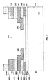
- FIG. 4 shows a cross section of an implementation of a sensor well.
- This sensor well may be fabricated on a silicon substrate using a CMOS process.
- the sensor material will fill and be constrained by a sensor well 410.
- the following layers may be patterned and used to form sensor well 410: a field oxide (fox) layer 420, a polysilicon (poly) layer 425, a first oxide (ox1) layer 430, a metal-1 (M1) layer 435, a second oxide (ox2) layer 440, a metal-2 (M2) layer 445, and a passivation or glass (GLAS) layer 450.
- fox field oxide
- poly polysilicon
- M1 metal-1
- ox2 metal-2
- GLAS passivation or glass
- An example of a process flow for fabricating a sensor well is as follows. An oxide layer is formed over a silicon substrate. A metal or conductive layer is formed on the oxide layer. The metal layer is patterned and etched. The resulting metal is to be used as contacts for the sensor material. An oxide layer is formed on the structure. A sensor well is patterned and etched. The sensor material is deposited in the sensor well and is in electrical contact with the patterned metal layer.
- the sensor material is applied to the sensor well after the sensor well is formed as a step during the fabrication of the chip (before the formation of the passivation layer).
- the sensor material may be applied at the semiconductor fabrication facility.
- the sensor material may be applied in a postprocessing step, after the fabrication of the chip.
- the sensor material is applied after the completed wafers are received from the semiconductor fabrication facility.
- the silicon substrate 415 is about 500 microns thick.
- the field oxide layer 420 is about 0.6 microns thick.
- the polysilicon layer 425 is about 0.4 microns thick.
- the first oxide layer 430 is about 0.85 microns thick.
- the metal-1 layer 435 is about 0.6 microns thick.
- the second oxide layer 440 is about 0.65 microns thick.
- the metal-2 layer 445 is about 1.15 microns thick.
- the passivation layer 350 is about 1 micron thick.
- a sensor well may be fabricated using a single-layer metal process and also processes having more than two layers of metal.
- a sensor well of the present invention may be fabricated in a process having three, four, five, or more layers of metal.
- connections 460 and 470 are formed in the metal-1 layer to make electrical contact with the sensor material. These electrical connections are used to route the sensor signals to other circuitry for further processing of sensor data. This circuitry may be on-chip or off-chip.
- the metal conductor used to form connections 460 and 470 is typically a conductive material such as gold, platinum, aluminum, or copper.
- the material for the electrical connections 460 and 470 should be selected so they are not reactive to the sensor material. In the case when the sensor material is applied during a postprocessing step, connections 460 and 470 will be exposed, and a conductive material such as aluminum may easily oxidize. This may result in poor electrical connections to the sensor material.
- Good electrical contacts are more important for some embodiments of the present invention than others.
- a good physical contact may be important when measuring the resistance of the sensor material. This is especially true in cases when the sensor material has a relatively low resistance when compared to the contact resistance.
- connections may be made by using a capacitive connection, where there is no physical connection between the sensor material and the conductive material or metal. Consequently, in such an embodiment, there would be fewer concerns associated with oxidation of the metal connection.
- the metal-1 layer may be, for example, postprocessed or at least finished in a nonstandard integrated circuit fashion.
- the surface of standard integrated circuit metalization is normally covered by a thin, air forming, "native" oxide layer.
- Aluminum the most popular standard metal, forms aluminum oxide continuously over its surface very quickly when exposed to air.
- Polymer/carbon black composite resistors can not be taken to high temperatures nor can they be energetically formed in other ways to break through the "native" oxide. As such, a means for good contact to the metal layer must be made. This could be accomplished by chemically or physically etching the exposed electrodes and keeping the metal-1 in an oxygen-free environment while applying the polymer composite sensor material.
- an additional layer, or multiple layer sandwich, whose exposed layer is a noble (nonoxidizing) metal may be deposited through any number of techniques on the surface of metal-1.
- This technique could be physical vapor deposition or chemical vapor deposition or plating amongst others.
- the technique of sputtering a gold contact layer over a chromium glue layer, followed by photo lithographically defining the metal sandwich is especially attractive.
- the circuitry receiving the sensor signals from connections 360 and 370 may be off-chip or on-chip.
- the other circuitry may include preprocessing, amplification, and classification of the sensor data.
- bonding pads may be formed along the periphery or edges of the chip, or may be distributed inside the chip (e.g., when using flip-chip packaging technology).
- the sensor well structure of Figure 4 may be used to constrain and allow measurement of the sensor material.
- the sensor material fills or partially fills sensor well 410, and resistance is measured using electrical connections 460 and 470.
- Figure 5 shows a top view of a 200-micron by 200-micron sensor well structure. Metal is used to make electrical connections 520 and 530 at opposite ends of the sensor well.
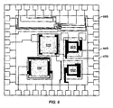
- Figure 6 shows a layout of a test structure with four sensor wells 610, 620, 630, and 640. These sensor wells are of various sizes. Specifically, sensor wells 620 and 640 are squares of 200 microns per side while sensor wells 610 and 630 are squares of 400 microns per side. Bonding pads 650 surround the four sensor wells and are electrically connected to the sensor wells. Two bonding pads or electrical connections may be used to connect to a particular sensor well. For example, pads 660 and 670 connect to the two terminals for sensor well 620. One bonding pad or electrical connection may be shared between two different sensor wells.
- Figure 7 shows a further embodiment of the present invention where electronic circuitry is formed below or beneath the sensor site.
- the figure shows a top view of a layout of the electronic devices at a sensor site. Electrical contacts 710 and 715 make electrical contact between the sensor material and electronic circuitry.
- the electronic devices implement a preprocessing circuit.
- the preprocessing circuit may include an autozeroing adaption circuit with signal amplification and X-Y decoding.
- the individual circuit blocks include a sensor read-out amplifier with baseline adaption circuit 720; signal amplification circuits 730, 735, and 740; and a row/column select and final output amplification circuit 750.
- electronic circuitry for any purpose may be implemented at or beneath the sensor site. Outputs from the electronic circuitry may be routed to other on-chip circuitry, or off-chip circuitry via the bonding pads.
- the sensor site is a 200-micron by 200-micron sensor well.
- the sensor material may be constrained at the sensor site using a structure or technique other than a sensor well.
- electronic circuitry is not necessarily formed beneath the sensor site, and may be placed anywhere on the same integrated circuit chip.
- electronic circuitry may be formed adjacent to the sensors, or in another location on the chip.
- an advantage of forming electronic circuitry beneath the sensors is that the resulting layout is relatively compact.
- a cross-sectional structure for the embodiment of Figure 7 may be similar to what is shown in Figure 4 where the electrical devices are formed using metal-1 and polysilicon layers.
- the second oxide layer will not be etched through.
- the second oxide layer will instead form a "bottom" for the sensor well.
- the metal-1 layer is used to electrically connect to the sensor material at the sensor site.
- Figures 8A through 8F show the different stages in the microfabricating a sensor well structure.
- the technique shown in Figure 8A through 8F may be an alternative to a CMOS semiconductor process.
- the process may be a MEMS or microelectrical fabrication process or other specialized VLSI process.
- the process may include micromachining to form the structures to constrain the sensor material.
- a starting wafer or substrate is shown in 8A.
- This layer is either an insulating substrate or a starting wafer to which has been added an insulating film. This can be either through oxidation (for a silicon substrate) or deposition.
- a conductive film may be deposited onto the insulating surface by either physical or chemical vapor deposition methods shown in Figure 8B.
- the metal or conductive film is patterned in Figure 8C leaving a pair of electrodes.
- An additional insulating film is deposited in Figure 8D and patterned to expose the electrodes of a nonoxidized metal structure in Figure 8E.
- the sensor material shown in Figure 8F.
- Sensor materials of diverse compositions are applied at the sensor sites of the chip.
- the sensor material may be deposited at the sensor sites by using solution spin coating or deposition of monomers and then polymerizing them.
- the polymer-based chemiresistors may be formed by spin- or dip-coating substrates with solutions or suspensions of the chemiresistor components.
- the need for diversity dictates there be a patterning of the first sensor material followed by the application and patterning of many subsequent layers. While not unfeasible, the number of times that this process need be repeated is dictated by the degree of diversity that is desired in the sensors.
- Another technique to produce sensor sites containing sensor materials with diverse compositions is to deposit the sensor material serially in time. This will involve making a first deposition at a site which contains a distinct chemical composition from the second, from the third, and so forth.
- a still further technique for applying the sensor material is to use microjet or ink jet technology.
- Ink jet technology is increasingly being used in the fabrication of devices. With such technology, it is possible to fabricate polymeric structures on the order of 100 microns and arrays of these structures with packing densities of greater than 15,000 per square centimeter. Microjets may be useful tools in fabricating large arrays of miniaturized sensors for analyte detection.
- a continuous jet system may be employed because the composition of the "ink” (e.g., the sensor material which may be a chemical polymer) can be continuously changed.
- the composition of the "ink” e.g., the sensor material which may be a chemical polymer
- This allows for the fabrication of sensor material films with variable composition from a limited feedstock of monomers or polymers as desired.
- the monomers delivered into the sensor sites would be polymerized in situ in a subsequent step through exposure to gamma irradiation, to a suitable free radical catalyst or by exposure to light. In this fashion, it will be possible to prepare libraries of thousands of different polymers from uncorrelated monomeric precursors, and to rapidly evaluate their efficacy in distinguishing the analytes of concern.
- microjet technology When using microjet technology, it is important to prevent the ink jet nozzles from clogging. It is desirable for the particle size of the ink be smaller than the nozzle size.
- microjet technology may be used to apply polymers with carbon black.
- classic black inks (such as India ink) are carbon black suspensions.
- the nozzle size of commercial ink jets is generally greater than ten microns. Since a stable carbon black suspension with particle sizes of less than one micron may be formed, it is possible to fabricate carbon black suspensions compatible with microjet technology.
- FIGs. 7G shows a cross section of a portion of an integrated circuit 700 according to this further embodiment.
- An advantage of this method is that it is highly flexible, and might be used with any number of different base integrated circuit processes. For example, this method is especially useful for those applications which require addressing the array a bit at a time, because many such addressable array architectures have been developed in silicon technology, and this technique allows one to make use of these previously developed infrastructures.
- a plurality of semiconductor devices 905 are formed within a substrate 910 by any conventional VLSI fabrication processes, as is well-known in the art.
- Conductors 915 are formed in a conductive layer to interconnect semiconductor devices 905 and to provide routing to the various sensors.
- Semiconductor devices 905 and conductors 915 are interconnected to form the various electronics on integrated circuit 900. For example, they may form the electronics for addressing and activating an array of sensor elements.
- Conductors 915 may be, for example, polysilicon, metal (e.g., aluminum or copper), or other conductive layers.
- two layers of metal are used for a bias to be generated and current measured at a given X-Y location in the array. Since the information that provides a signal is the change in the resistance of a node, the access lines can be relatively high impedance without causing any serious loss of signal or inducing much additional Johnson noise.
- the polysilicon layer available in every CMOS technology, is usable. In a typical scenario, with a hundred squares of resistance at 10 ohms per square, a polysilicon line might be on the order 1000 ohms of fixed resistance in series with the signal resistor.
- Insulator layer 920 of SiO 2 , SiOxN 4 , or other insulating material is formed above semiconductor device 910. Insulator layer 920 electrically isolates semiconductor devices 910 and conductors 915. Contacts 730 are formed within insulator layer 920 to allow electrical connections to conductors 915, and may be formed of a variety of conductive materials such as tungsten or other refractory metals. Although only one contact 930 is shown in Figure 9 for simplicity, it will be recognized that each sensor may have more than one contact 930 connected to it, for example, to use the contact as a resistive element between two conductors.
- integrated circuit 900 is planarized to provide a substantially flat surface.
- the planarization may be accomplished, for example, using chemical-mechanical processing (CMP), a technique well known in the art of integrated circuit processing.
- CMP chemical-mechanical processing
- contacts 930 are exposed.
- Contacts 930 having exposed metal may be covered with an optional noble metal coating 935 through physical vapor deposition, chemical vapor deposition, or plating techniques to provide an optimal electrical contact.
- a polymer forming a sensor 940 of the type described above is deposited on contact 915 (or noble metal coating 935 if provided).
- contact 915 or noble metal coating 935 if provided.
- thousands of sensors 940 might be made by varying the composition of two, three, four, or more different types of polymers. A flat surface for this purpose would be desirable.
- a second insulator layer 950 may be provided with opening for sensors 940.
- Insulator layer 950 is preferably Teflon® (a trademark of E.I. DuPont de Nemours and Company), Teflon®-like material, or other fluoropolymer, although other insulators may be used.
- Teflon® a trademark of E.I. DuPont de Nemours and Company
- Teflon®-like material or other fluoropolymer
- sensors 940 can become the determinant of the size of the chip if each sensor 940 has to be isolated physically from every other sensor 940. In this case, the dilution of the solution used to cast sensor 940 is desired to be as high as possible. The thinner the film the finer the degree to which it can be patterned or physically localized by other means.
- sensor 940 should be as thin as possible without destroying its electrical properties. If the desired thickness of the polymer film becomes smaller than the conductive particle size, solution casting becomes impractical.
- sensors 940 are formed by putting the conductive particles down and then coating the conductive particles with the polymer films through a vapor deposition process. In some embodiments, these films may be made with no polymer at all, and yet still be sensitive to analytes. By putting down the conductive particles first and then coating them with a thin film of polymer, one could have an effective active film arbitrarily thin supported by the larger conductive particles in a porous configuration.
- sensor 940 is formed by making a porous particle film with polymer coating the particles. This improves the response much faster and the lateral dimensions determined by the localization of a polymer vapor deposition.
- Another response time enhancement is to make sensor 940 with an inert or sacrificial particle filler which is either very permeable or removable after deposition. While this does not change the thickness parameter positively, in some cases it is a simpler way to achieve the response time benefits of the spongy film detailed above with the application techniques that are in use today.
- Figure 10 is a cross-sectional diagram showing another example of a sensor element of the present invention created by another method.
- This technique also benefits from the planarized integrated circuit described with respect to Figure 9.
- semiconductor devices 1005, conductors 1010, and contacts 1030 are formed and the integrated circuit is planarized as described above, and optional noble metal coating 1035 is formed above contact 1030.
- micromachining techniques are used to form high, hurdle-like structures 1060.
- a polymer film 1065 is deposited onto hurdle-like structure 1060 with a thickness that may be determined by the surface tension or wetting properties of the polymer, solvent conductive particle mixture, rather than the volume in the drop or dispensed amount. This allows the sensor to be thinner, the response faster and the silicon area to be reduced.
- Figure 11 shows another embodiment of the present invention that may take advantage of the planarization technique described above with respect to Figure 9.
- a very high impedance film 1180 is placed across semiconductor devices (not shown in Figure 11) that form the array.
- Chemisensitive sensors 1185 are deposited right on top of high impedance film 1180 forming a distributed parallel resistor. This allows working in a domain of thinness where the actual signal generating film does not need to be continuous. Even if short segments change, the terminal resistances within the array would be impacted.
- FIG. 12 the equivalent circuit for the case of a discontinuous film on top of a continuous high-impedance film is shown in Figure 12.
- the high impedance film is represented by leg B in the drawing or as a continuous resistor.
- Leg A of the drawing shows a group of variable resistors that are in parallel with the underlying resistor.
- Figure 13 is a block diagram of an embodiment of the present invention that measures a capacitance of the sensor material to determine the presence of an analyte. While Figure 13 shows only a single pair of sensors, the circuitry may also be expanded to include an array of sensors or an array of pairs of sensors. Each sensor in the array may include a different type of sensor material from other sensors as described above.
- Capacitance may be measured in a variety of ways.
- Figure 13 depicts one such method. However, other circuitry for measuring capacitance may be substituted for the circuitry shown.
- two sensors 1310 and 1320 are provided. Sensors 1310 and 1320 are sensors formed substantially identical to one another. However, sensor 1410 is exposed such that analytes may penetrate the sensor material and cause it to expand. On the other hand, sensor 1320 is covered by an insulator layer so that it will not be affected by analytes. As such, sensor 1320 is a reference sensor, and its capacitance can be compared with the capacitance of sensor 1310 to determine if sensor 1320 has expanded due to the presence of an analyte.
- Frequency generators 1330 and 1332 are coupled to sensors 1310 and 1320, respectively, through contacts 1340 and 1342.
- Frequency generators 1330 and 1332 output an oscillating signal at a particular frequency, and receive back return signals f1 and f2.
- Return signals f1 and f2 may be phase-shifted or frequency shifted, depending upon the capacitance of the sensor.
- the capacitance is the same as that of sensor 1320 and f1 is the same as f2.
- the capacitance of sensor 1320 is greater, and thus f1 is not the same as f2.
- the difference between f1 and f2 may be used to determine the change in capacitance.
- the return signals f1 and f2 are input to a discriminator mixer 1350.
- Discriminator mixers are well known in the electrical arts, and in particular for example, in the design of phase locked loops.
- Mixer 1350 receives two frequencies, and outputs a DC output that is zero if the frequencies are the same, and nonzero if the frequencies are different. The greater the frequency difference, the higher the value of the DC output.
- the output of mixer 1350 is zero, then the capacitance of the two sensors are the same, and no analyte is present; if the magnitude of the output is nonzero, then an analyte is present, and may be identified by the value of the DC output.
- capacitance measuring circuitry may also be used.
- two similar adjacent sensors may be formed such that they have room to expand in a sideways direction.
- Each of the two sensors are coupled to a different conductive trace, and the sensors are coupled through the conductive trace to a capacitance measuring circuit.
- the sensors When no analyte is present, the sensors have a certain separation, that is known, and thus has a known capacitance.
- the sensors expand and the distance between them shortens causing the capacitance to change. By measuring the change in capacitance, the presence of the analyte may be determined.
- Figure 14 shows another embodiment of the present invention for measuring the capacitance of a sensor element.
- sensors 1410 and 1420 are substantially identical.
- a capacitive measuring device 1430 coupled to sensor 1410 by two conductors 1440 and 1442 through contacts or otherwise.
- the capacitive measuring device is any device capable of determining a capacitance of sensor 1410.
- a second capacitance measuring device is coupled to sensor 1420 through two conductors 1460 and 1462.
- Sensor 1420 is isolated from exposure to analytes, while sensor 1410 may be exposed to them.
- a comparator 1470 compares the capacitances measured from the two sensors 1410 and 1420. These values may be analyzed by various techniques described above or otherwise.
- Figure 15 shows an integrated circuit layout that may be used for the circuit shown in Figure 14.
- Conductors 1540 and 1542 are interdigitated on the integrated circuit. These conductors are associated with one capacitor.
- Sensor 1510 is formed above the interdigitated conductors.
- sensor 1520 is formed above interdigitated conductors 1560 and 1562. These conductors are associated with another capacitor.
- Figure 16 shows a "unit cell" 1610 for a sensor of the analyte detection chip of the present invention.
- unit cell 1610 may be repeated as many times as desired. For example, for an analyte detection chip with ten sensors, the unit cell is repeated ten times. For an analyte detection chip with thirty sensors, the unit cell is repeated thirty times. For a chip with 100 sensors, the unit cell is repeated 100 times. For a chip with "n" sensors, the unit cell is repeated at least "n" times.
- unit cell 1610 includes sensor 1620 by itself. Electrical connections from the unit cell will be connected to other electronic circuitry, on-chip or off-chip, for further processing.
- a first of the chips may contain a plurality of sensors 1620 and their respective electrical connections.
- a second of the chips may be electrically coupled to sensors 1620 to process the signals from the sensors on the first chip.
- a more highly integrated embodiment of unit cell 1610 includes sensor 1620 and electronics 1630, both on the same chip or substrate.
- Electronics 1630 may be formed beneath the sensor site of sensor 1620, as was described for Figure 4 above.
- Electronics 1630 are electrically coupled to sensor 1620 by connections 1640 and 1650.
- Electronics 1630 processes the signals from the sensor. The processing includes amplification or filtering, or both.
- An output 1660 of the electronics may be coupled to other circuitry 1670 for even further processing.
- the other circuitry may be off-chip for classifying the analyte.
- Figure 17 shows an embodiment of circuitry for reading out a sensor array.
- the array of chemically sensitive sensors is shown in this embodiment as variable resistors, each connected between a row bias line and a column read line.
- a row and a column multiplexer are to "sample" the sensor data in a scheme somewhat like to scanning a television picture.
- a row address is translated into the application of bias (i.e., iBias) to one row, and the column address is translated into the closure of a column read switch switching the output to a load resistor that is at the input of an analog-to-digital (A/D) converter whose output is in turn fed to the controller of the system.
- bias i.e., iBias
- A/D analog-to-digital
- dummy rows and columns of sensors which is a row or column of sensors is formed but not used functionally as are active rows and columns of sensors.
- dummy rows and columns of sensors may be formed at row and column edges of the array. These dummy rows and columns of sensors may be used to ensure the active interior row and columns of sensors are relatively uniform, since sensors at the edge may exhibit some edge effects by not having a similar number of adjacent sensors as for the interior sensors.
- Dummy rows and columns may also be used in a redundancy scheme when these are activated, possibly by laser programming or programming of nonvolatile or one-time programmable memory elements such as Flash, EEPROM, EPROM, or antifuse cells. These dummy row and columns may be used in the place of other rows and columns that are or have become defective. For example, a redundancy scheme may help improve the yield of good die, or increase the service life of an analyte detection chip.
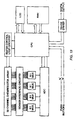
- FIG. 18 shows a block diagram of an analyte detection system.
- the block diagram for a discrete system that has been developed are shown in the analyte detection system block diagram and system design.
- Any full analyte sampling system should include a means for sampling the analyte of interest. This could be as simple as a stick to attach the sensors and a means for holding it in the vicinity of a vapor of interest, or as complex as a network of pumps and valves sequencing through a complex sampling routine.
- the analyte has been presented to the array of chemically sensitive transducers, the signals are processed and presented to an A/D converter.
- the pattern of response across the array is then compared to a stored pattern of response and an identification can be made through any number of possible input output channels as simple as wires to a control system or as complex as a visual display system.
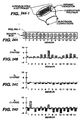
- FIG 19 shows a block diagram of a specific embodiment of an analyte system of the present invention.
- a particular embodiment of such a system is shown in the block diagram of a system that has been implemented in a discrete design.
- the signals are buffered, and each bank of eight sensor signals is then fed through an 8-to-1 analog multiplexer to an A/D that has an additional 4-to-1 multiplexer internal to it.
- the data is streamed out of the A/D converter in a serial bit stream to a central processing unit (CPU).
- the CPU may be a computer.
- the CPU additionally is interfaced to a heater control system.
- the chemically sensitive sensors are also temperature dependant, controlling the temperature in the system eliminates one source of noise.
- the data is stored by the CPU in random access memory (RAM) or in another storage media such as magnetic disk.
- RAM random access memory
- the measurements can be compared to a learned pattern of response previously stored and the CPU can calculate the best match and report the result through the LCD panel display.
- the number of sensors grows beyond thirty-two, the number of connections can become impractical to make with solder or other physical attachment processes. More of the block diagram will then be integrated onto a chip since the wiring connections inside and integrated circuit are very reliable. As the number of sensors approaches 100, it makes economic sense to integrate a matrix measurement scheme on the same substrate as the sensors. As the number of sensors grows even further, the A/D converter can become overtaxed and more than one makes sense to keep the system throughput in the range of one second where the flow system time constant becomes the limitation to overall system response. As the number of sensors grows to an even larger number, the A/D technology needs to be changed to either a large array of slower A/Ds or a faster variety of converter or both. With an array of A/D converters on the chip a digital multiplexer needs to be added to funnel the outputs through to the CPU. As the number of sensor elements climbs to the millions, some condensation of the data needs to take place within the array itself.
- the field of the invention is electrical sensors for detecting analytes in fluids.
- the invention provides methods, apparatuses and expert systems for detecting analytes in fluids.
- the apparatuses include a chemical sensor comprising first and second conductive elements (e . g ., electrical leads) electrically coupled to a chemically sensitive resistor which provides an electrical path between the conductive elements.
- the resistor comprises a plurality of alternating nonconductive regions (comprising a nonconductive organic polymer) and conductive regions (comprising a conductive material).
- the electrical path between the first and second conductive elements is transverse to ( i.e. , passes through) said plurality of alternating nonconductive and conductive regions.
- the resistor provides a difference in resistance between the conductive elements when contacted with a fluid comprising a chemical analyte at a first concentration, than when contacted with a fluid comprising the chemical analyte at a second different concentration.
- any given nonconductive region is typically on the order of 100 angstroms in length, providing a resistance of on the order of 100 m ⁇ across the region.
- Variability in chemical sensitivity from sensor to sensor is conveniently provided by qualitatively or quantitatively varying the composition of the conductive and/or nonconductive regions.
- the conductive material in each resistor is held constant (e . g ., the same conductive material such as polypyrrole) while the nonconductive organic polymer varies between resistors ( e . g ., different plastics such as polystyrene).
- Arrays of such sensors are constructed with at least two sensors having different chemically sensitive resistors providing dissimilar differences in resistance.
- An electronic nose for detecting an analyte in a fluid may be constructed by using such arrays in conjunction with an electrical measuring device electrically connected to the conductive elements of each sensor.
- Such electronic noses may incorporate a variety of additional components including means for monitoring the temporal response of each sensor, assembling and analyzing sensor data to determine analyte identity, etc.
- the invention provides sensor arrays for detecting an analyte in a fluid for use in conjunction with an electrical measuring apparatus.
- These arrays comprise a plurality of compositionally different chemical sensors.
- Each sensor comprises at least first and second conductive leads electrically coupled to and separated by a chemically sensitive resistor.
- the leads may be any convenient conductive material, usually a metal, and may be interdigitized to maximize signal-to-noise strength.
- the electrical property of interest for the chemical sensor material is resistance.
- the chemical sensor material has other electrical properties including capacitance and inductance.
- the sensor material exhibits a swelling phenomenon that may be measured by changes in any electrical property such as resistance, capacitance, or inductance, or combinations of these properties.
- detecting analytes may be accomplished by evaluating a capacitance of the sensor material.
- the resistor comprises a plurality of alternating nonconductive and conductive regions transverse to the electrical path between the conductive leads.
- the resistors are fabricated by blending a conductive material with a nonconductive organic polymer such that the electrically conductive path between the leads coupled to the resistor is interrupted by gaps of non-conductive organic polymer material.
- the matrix regions separating the particles provide the gaps.
- the nonconductive gaps range in path length from about 10 to 1,000 angstroms, usually on the order of 100 angstroms providing individual resistance of about 10 to 1,000 m ⁇ , usually on the order of 100 m ⁇ , across each gap.
- the path length and resistance of a given gap is not constant but rather is believed to change as the nonconductive organic polymer of the region absorbs, adsorbs or imbibes an analyte. Accordingly the dynamic aggregate resistance provided by these gaps in a given resistor is a function of analyte permeation of the nonconductive regions.
- the conductive material may also contribute to the dynamic aggregate resistance as a function of analyte permeation ( e . g ., when the conductive material is a conductive organic polymer such as polyprryole).
- conductive materials and nonconductive organic polymer materials can be used.
- Table 1 provides exemplary conductive materials for use in resistor fabrication; mixtures, such as of those listed, may also be used.
- Table 2 provides exemplary nonconductive organic polymer materials; blends and copolymers, such as of the polymers listed here, may also be used. Combinations, concentrations, blend stoichiometries, percolation thresholds, etc. are readily determined empirically by fabricating and screening prototype resistors (chemiresistors) as described below.
- Organic Conductors conducting polymers poly(anilines), poly(thiophenes), poly(pyrroles), poly(acetylenes), etc .)), carbonaceous materials (carbon blacks, graphite, coke, C 60 , etc. ), charge transfer complexes (tetramethylparaphenylenediami- ne-chloranile, alkali metal tetracyanoquinodimethane complexes, tetrathiofulvalene halide complexes, etc.), etc.
- Inorganic Conductors metals and metal alloys (Ag, Au, Cu, Pt, AuCu alloy, etc .), highly doped semiconductors (Si, GaAs, InP, MoS 2 , TiO 2 , etc.), conductive metal oxides (In 2 O 3 , SnO 2 , Na x Pt 3 O 4 , etc.), superconductors (YBa 2 Cu 3 O 7 , Tl 2 Ba 2 Ca 2 Cu 3 O 10 , etc. ), etc .
- Mixed inorganic/organic Conductors Tetracyanoplatinate complexes, Iridium halocarbonyl complexes, stacked macrocyclic complexes, etc .
- Main-chain carbon polymers poly(dienes), poly(alkenes), poly(acrylics), poly(methacrylics), poly(vinyl ethers), poly(vinyl thioethers), poly(vinyl alcohols), poly(vinyl ketones), poly(vinyl halides), poly(vinyl nitriles), poly (vinyl esters), poly(styrenes), poly(arylenes), etc .
- Main-chain acyclic heteroatom polymers poly(oxides), poly(carbonates), poly(esters), poly(anhydrides), poly(urethanes), poly(sulfonates), poly(siloxanes), poly(sulfides), poly(thioesters), poly(sulfones), poly(sulfonamides), poly(amides), poly(ureas), poly(phosphazenes), poly(silanes), poly(silazanes), etc .
- Main-chain Heterocyclic polymers poly(furan tetracarboxylic acid diimides), poly(benzoxazoles), poly(oxadiazoles), poly(benzothiazinophenothiaz ines), poly(benzothiazoles), poly(pyrazinoquinoxalines), poly(pyromellitimides), poly(quinoxalines), poly(benzimidazoles), poly(oxindoles), poly(oxoisoindolines), poly(dioxoisoindolines), poly(triazines), poly(pyridazines), poly(piperazines), poly(pyridines), poly(piperidines), poly(triazoles), poly(pyrazoles), poly(pyrrolidines), poly(carboranes), poly(oxabicyclononanes), poly(dibenzofurans), poly(phthalides), poly(acetals), poly(anhydrides), carbohydrates, etc .
- the chemiresistors can be fabricated by many techniques such as, but not limited to, solution casting, suspension casting, and mechanical mixing.
- solution cast routes are advantageous because they provide homogeneous structures and ease of processing.
- resistor elements may be easily fabricated by spin, spray or dip coating. Since all elements of the resistor must be soluble, however, solution cast routes are somewhat limited in their applicability.
- Suspension casting still provides the possibility of spin, spray or dip coating but more heterogeneous structures than with solution casting are expected.
- mechanical mixing there are no solubility restrictions since it involves only the physical mixing of the resistor components, but device fabrication is more difficult since spin, spray and dip coating are no longer possible. A more detailed discussion of each of these follows.
- the chemiresistors can be fabricated by solution casting.
- the oxidation of pyrrole by phosphomolybdic acid presented herein represents such a system.
- the phosphomolybdic acid and pyrrole are dissolved in tetrahydrofuran (THF) and polymerization occurs upon solvent evaporation.
- THF tetrahydrofuran
- the choice of non-conductive polymers in this route is, of course, limited to those that are soluble in the reaction media.
- the doping procedure exposure to I 2 vapor, for instance
- the doping procedure can be performed on the blend to render the substituted poly(cyclooctatetraene) conductive.
- the choice of non-conductive polymers is limited to those that are soluble in the solvents that the undoped conducting polymer is soluble in and to those stable to the doping reaction.
- Certain conducting polymers can also be synthesized via a soluble precursor polymer. In these cases, blends between the precursor polymer and the non-conducting polymer can first be formed followed by chemical reaction to convert the precursor polymer into the desired conducting polymer. For instance poly( p -phenylene vinylene) can be synthesized through a soluble sulfonium precursor.
- Blends between this sulfonium precursor and the non-conductive polymer can be formed by solution casting. After which, the blend can be subjected to thermal treatment under vacuum to convert the sulfonium precursor to the desired poly( p -phenylene vinylene).
- suspension casting In suspension casting, one or more of the components of the resistor is suspended and the others dissolved in a common solvent. Suspension casting is a rather general technique applicable to a wide range of species, such as carbon blacks or colloidal metals, which can be suspended in solvents by vigorous mixing or sonication.
- the non-conductive polymer is dissolved in an appropriate solvent (such as THF, acetonitrile, water, etc.). Colloidal silver is then suspended in this solution and the resulting mixture is used to dip coat electrodes.
- an appropriate solvent such as THF, acetonitrile, water, etc.
- the individual elements can be optimized for a particular application by varying their chemical make up and morphologies.
- the chemical nature of the resistors determines to which analytes they will respond and their ability to distinguish different analytes.
- the relative ratio of conductive to insulating components determines the magnitude of the response since the resistance of the elements becomes more sensitive to sorbed molecules as the percolation threshold is approached.
- the film morphology is also important in determining response characteristics. For instance, thin films respond more quickly to analytes than do thick ones.
- sensors can be chosen that are appropriate for the analytes expected in a particular application, their concentrations, and the desired response times. Further optimization can then be performed in an iterative fashion as feedback on the performance of an array under particular conditions becomes available.
- the resistor may itself form a substrate for attaching the lead or the resistor.
- the structural rigidity of the resistors may be enhanced through a variety of techniques: chemical or radiation cross-linking of polymer components (dicumyl peroxide radical cross-linking, UV-radiation cross-linking of poly(olefins), sulfur cross-linking of rubbers, e-beam cross-linking of Nylon, etc.), the incorporation of polymers or other materials into the resistors to enhance physical properties (for instance, the incorporation of a high molecular weight, high transition metal (Tm) polymers), the incorporation of the resistor elements into supporting matrices such as clays or polymer networks (forming the resistor blends within poly(methylmethacrylate) networks or within the lamellae of montmorillonite, for instance), etc.
- the resistor is deposited as a surface layer on a solid matrix which provides means for supporting the leads.
- the matrix is a chemically inert, non-conductive
- Sensor arrays particularly well-suited to scaled up production are fabricated using integrated circuit (IC) design technologies.
- IC integrated circuit
- the cheroiresistors can easily be integrated onto the front end of a simple amplifier interfaced to an A/D converter to efficiently feed the data stream directly into a neural network software or hardware analysis section.
- Micro-fabrication techniques can integrate the chemiresistors directly onto a micro-chip which contains the circuitry for analogue signal conditioning/processing and then data analysis. This provides for the production of millions of incrementally different sensor elements in a single manufacturing step using ink-jet technology. Controlled compositional gradients in the chemiresistor elements of a sensor array can be induced in a method analogous to how a color ink-jet printer deposits and mixes multiple colors.
- a sensor array of a million distinct elements only requires a 1 cm x 1 cm sized chip employing lithography at the 10 ⁇ m feature level, which is within the capacity of conventional commercial processing and deposition methods. This technology permits the production of sensitive, small-sized, stand-alone chemical sensors.
- Preferred sensor arrays have a predetermined inter-sensor variation in the structure or composition of the nonconductive organic polymer regions.
- the variation may be quantitative and/or qualitative.
- concentration of the nonconductive organic polymer in the blend can be varied across sensors.
- a variety of different organic polymers may be used in different sensors.
- An electronic nose for detecting an analyte in a fluid is fabricated by electrically coupling the sensor leads of an array of compositionally different sensors to an electrical measuring device.
- the device measures changes in resistivity at each sensor of the array, preferably simultaneously and preferably over time.
- the device includes signal processing means and is used in conjunction with a computer and data structure for comparing a given response profile to a structure-response profile database for qualitative and quantitative analysis.
- a nose comprises at least ten, usually at least 100, and often at least 1000 different sensors though with mass deposition fabrication techniques described herein or otherwise known in the art, arrays of on the order of at least 10 6 sensors are readily produced.
- each resistor provides a first electrical resistance between its conductive leads when the resistor is contacted with a first fluid comprising a chemical analyte at a first concentration, and a second electrical resistance between its conductive leads when the resistor is contacted with a second fluid comprising the same chemical analyte at a second different concentration.
- the fluids may be liquid or gaseous in nature.
- the first and second fluids may reflect samples from two different environments, a change in the concentration of an analyte in a fluid sampled at two time points, a sample and a negative control, etc.
- the sensor array necessarily comprises sensors which respond differently to a change in an analyte concentration, i.e., the difference between the first and second electrical resistance of one sensor is different from the difference between the first second electrical resistance of another sensor.
- the temporal response of each sensor is recorded.
- the temporal response of each sensor may be normalized to a maximum percent increase and percent decrease in resistance which produces a response pattern associated with the exposure of the analyte.
- a structure-function database correlating analytes and response profiles is generated. Unknown analyte may then be characterized or identified using response pattern comparison and recognition algorithms.
- analyte detection systems comprising sensor arrays, an electrical measuring devise for detecting resistance across each chemiresistor, a computer, a data structure of sensor array response profiles, and a comparison algorithm are provided.
- the electrical measuring device is an integrated cicuit comprising neural network-based hardware and a digital-analog converter (DAC) multiplexed to each sensor, or a plurality of DACs, each connected to different sensor(s).
- DAC digital-analog converter
- analytes and fluids may be analyzed by the disclosed sensors, arrays and noses so long as the subject analyte is capable generating a differential response across a plurality of sensors of the array.
- Analyte applications include broad ranges of chemical classes such as organics such as alkanes, alkenes, alkynes, dienes, alicyclic hydrocarbons, arenes, alcohols, ethers, ketones, aldehydes, carbonyls, carbanions, polynuclear aromatics and derivatives of such organics, e . g ., halide derivatives, etc. , biomolecules such as sugars, isoprenes and isoprenoids, fatty acids and derivatives, etc .
- commercial applications of the sensors, arrays and noses include environmental toxicology and remediation, biomedicine, materials quality control, food and agricultural products monitoring, etc.
- the general method for using the disclosed sensors, arrays and electronic noses, for detecting the presence of an analyte in a fluid involves resistively sensing the presence of an analyte in a fluid with a chemical sensor comprising first and second conductive leads electrically coupled to and separated by a chemically sensitive resistor as described above by measuring a first resistance between the conductive leads when the resistor is contacted with a first fluid comprising an analyte at a first concentration and a second different resistance when the resistor is contacted with a second fluid comprising the analyte at a second different concentration.
- Poly(pyrrole) films used for conductivity, electrochemical, and optical measurements were prepared by injecting equal volumes of N 2 -purged solutions of pyrrole (1.50 mmoles in 4.0 ml dry tetrahydrofuran) and phosphomolybdic acid (0.75 mmoles in 4.0 ml tetrahydrofuran) into a N 2 -purged test tube. Once the two solutions were mixed, the yellow phosphomolybdic acid solution turned dark green, with no observable precipitation for several hours. This solution was used for film preparation within an hour of mixing.
- Plasticized poly(pyrrole) sensors were made by mixing two solutions, one of which contained 0.29 mmoles pyrrole in 5.0 ml tetrahydrofuran, with the other containing 0.25 mmoles phosphomolybdic acid and 30 mg of plasticizer in 5.0 ml of tetrahydrofuran. The mixture of these two solutions resulted in a w:w ratio of pyrrole to plasticizer of 2:3.
- An inexpensive, quick method for crating the chemiresistor array elements was accomplished by effecting a cross sectional cut through commercial 22 nF ceramic capacitors (Kemet Electronics Corporation).
- a data set obtained from a single exposure of the array to an odorant produced a set of descriptors (i.e., resistances), d i .
- the data obtained from multiple exposures thus produced a data matrix D where each row, designated by j, consisted of n descriptors describing a single member of the data set ( i . e ., a single exposure to an odor). Since the baseline resistance and the relative changes in resistance varied among sensors, the data matrix was autoscaled before further processing (19). In this preprocessing technique, all the data associated with a single descriptor ( i .
- d' ij (d ij - d i )/ ⁇ i where d i is the mean value for descriptor i and ⁇ i is the corresponding standard deviation.
- Principle component analysis (19) was performed to determine linear combinations of the data such that the maximum variance (defined as the square of the standard deviation) between the members of the data set was obtained in n mutually orthogonal dimensions.
- the linear combinations of the data resulted in the largest variance [or separation] between the members of the data set in the first principle component (pc1) and produced decreasing magnitudes of variance from the second to the n th principle component (pc2 - pcn).
- This operation produced the correlation matrix, R whose diagonal elements were unity and whose off-diagonal elements were the correlation coefficients of the data.
- the total variance in the data was thus given by the sum of the diagonal elements in R.
- the n eigenvalues, and the corresponding n eigenvectors, were then determined for R.
- Each eigenvector contained a set of n coefficients which were used to transform the data by linear combination into one of its n principle components.
- the corresponding eigenvalue yielded the fraction of the total variance that was contained in that principle component.
- This operation produced a principle component matrix, P, which had the same dimensions as the original data matrix. Under these conditions, each row of the matrix P was still associated with a particular odor and each column was associated with a particular principle component.
- Fig. 42 shows the cyclic voltammetric behavior of a chemically polymerized poly(pyrrole) film following ten cycles from -1.00 V to +0.70 V vs. SCE.
- the cathodic wave at -0.40 V corresponded to the reduction of poly(pyrrole) to its neutral, nonconducting state
- the anodic wave at -0.20 V corresponded to the reoxidation of poly(pyrrole) to its conducting state (24).
- Fig 23A shows the optical spectrum of a processed polypyrrole film that had been spin-coated on glass and then rinsed with methanol.
- the single absorption maximum was characteristic of a highly oxidized poly(pyrrole) (26), and the absorption band at 4.0 eV was characteristic of an interband transition between the conduction and valence bands.
- the lack of other bands in this energy range was evidence for the presence of bipolaron states (see Fig. 23A), as have been observed in highly oxidized poly(pyrrole) (26).
- Plasticizers used in array elements Sensor Plasticizer 1 None 2 none 3 poly(styrene) 4 poly(styrene) 5 poly(styrene) 6 poly(a-methyl styrene) 7 poly(styrene-acrylonitrile) 8 poly(styrene-maleic anydride) 9 poly(styrene-allyl alcohol) 10 poly(vinyl pyrrolidone) 11 poly(vinyl phenol) 12 poly(vinyl butral) 13 poly(vinyl acetate) 14 poly(carbonate)
- Sensor arrays consisted of as many as 14 different elements, with each element synthesized to produce a distinct chemical composition, and thus a distinct sensor response, for its polymer film.
- the resistance, R, of each film-coated individual sensor was automatically recorded before, during, and after exposure to various odorants.
- a typical trial consisted of a 60 sec rest period in which the sensors were exposed to flowing air (3.0 liter-min -1 ), a 60 sec exposure to a mixture of air (3.0 liter-min -1 ) and air that had been saturated with solvent (0.5 - 3.5 liter-min -1 ), and then a 240 sec exposure to air (3.0 liter-min -1 ).
- Figs. 4B-4D depict representative examples of sensor amplitude responses of a sensor array (see, Table 3).
- data were recorded for three separate exposures to vapors of acetone, benzene, and ethanol flowing in air.
- the response patterns generated by the sensor array described in Table 3 are displayed for: (B) acetone; (C) benzene, and (D) ethanol.
- the sensor response was defined as the maximum percent increase and decrease of the resistance divided by the initial resistance (gray bar and black bar, respectively) of each sensor upon exposure to solvent vapor. In many cases sensors exhibited reproducible increases and decreases in resistance.
- An exposure consisted of: (i) a 60 sec rest period in which the sensors were exposed to flowing air (3.0 liter-min -1 ); (ii) a 60 sec exposure to a mixture of air (3.0 liter-min -1 ) and air that had been saturated with solvent (0.5 liter-min -1 ); and (iii) a 240 sec exposure to air (3.0 liter-min -1 ). It is readily apparent that these odorants each produced a distinctive response on the sensor array.
- Fig. 26 shows the principle component analysis for all 14 sensors described in Table 3 and Figs. 24 and 25.
- Fig. 26A or 26B When the solvents were projected into a three dimensional odor space (Fig. 26A or 26B), all eight solvents were easily distinguished with the specific array discussed herein. Detection of an individual test odor, based only on the criterion of observing -1% ⁇ R max /R i values for all elements in the array, was readily accomplished at the parts per thousand level with no control over the temperature or humidity of the flowing air. Further increases in sensitivity are likely after a thorough utilization of the temporal components of the ⁇ R max /R i data as well as a more complete characterization of the noise in the array.
- the same sensor array was also able to resolve the components in various test methanol-ethanol mixtures (29). As shown in Fig. 27B, a linear relationship was observed between the first principle component and the mole fraction of methanol in the liquid phase, x m , in a CH 3 OH-C 2 H 5 OH mixture, demonstrating that superposition held for this mixture/sensor array combination. Furthermore, although the components in the mixture could be predicted fairly accurately from just the first principle component, an increase in the accuracy could be achieved using a multi-linear least square fit through the first three principle components. This relationship held for CH 3 OH/(CH 3 OH + C 2 H 5 OH) ratios of 0 to 1.0 in air-saturated solutions of this vapor mixture. The conducting polymer-based sensor arrays could therefore not only distinguish between pure test vapors, but also allowed analysis of concentrations of odorants as well as analysis of binary mixtures of vapors.
- This type of polymer-based array is chemically flexible, is simple to fabricate, modify, and analyze, and utilizes a low power dc resistance readout signal transduction path to convert chemical data into electrical signals. It provides a new approach to broadly-responsive odor sensors for fundamental and applied investigations of chemical mimics for the mammalian sense of smell. Such systems are useful for evaluating the generality of neural network algorithms developed to understand how the mammalian olfactory system identifies the directionality, concentration, and identity of various odors.
- a sensor exposure consisted of (1) a 60 second exposure to flowing air (6 liter min-1), (2) a 60 second exposure to a mixture of air (6 liter min-1) and air that had been saturated with the analyte (0.5 liter min-1), (3) a five minute recovery period during which the sensor array was exposed to flowing air (6 liter min-1).
- the resistance of the elements were monitored during exposure, and depending on the thickness and chemical make-up of the film, resistance changes as large as 250% could be observed in response to an analyte.
- Cited References 1. Lundström et al. (1991) Nature 352 :47-50; 2. Shurmer and Gardner (1992) Sens. Act. B 8 :1-11; 3. Reed (1992) Neuron 8 :205-209; 4. Lancet and Ben-Airie (1993) Curr. Biol . 3 :668-674; 5.
- a sensor array for detecting an analyte in a fluid for use in conjunction with an electrical measuring apparatus comprising at least first and second chemical sensors each comprising: at least first and second conductive leads suitable for electrical connection to the electrical measuring apparatus and electrically coupled to a chemically sensitive resistor comprising a plurality of alternating nonconductive regions comprising a nonconductive organic polymer and conductive regions comprising a conductive material compositionally different than said nonconductive organic polymer, said resistor providing an electrical path between said conductive leads and through said regions, a first electrical resistance between said conductive leads when said resistor is contacted with a first fluid comprising a chemical analyte at a first concentration, and a second electrical resistance between said conductive leads when said resistor is contacted with a second fluid comprising said chemical analyte at a second different concentration the difference between said first electrical resistance and said second electrical resistance of said first chemical sensor being different from the difference between said first electrical resistance and said second electrical resistance of said second chemical sensor.
- a sensor array wherein said conductive material is an inorganic conductor.
- a system for detecting an analyte in a fluid comprising: at least first and second chemical sensors each comprising at least first and second conductive leads electrically coupled to a chemically sensitive resistor comprising a plurality of alternating nonconductive regions comprising a nonconductive organic polymer and conductive regions comprising a conductive material compositionally different than said nonconductive organic polymer, said resistor providing an electrical path between said conductive leads and throught said regions, a first electrical resistance between said conductive leads when said resistor is contacted with a first fluid comprising a chemical analyte at a first concentration and a second different electrical resistance when said resistor is contacted with a second fluid comprising said chemical analyte at a second different concentration, the difference between said first electrical resistance and said second electrical resistance of said first chemical sensor being different from the difference between said first electrical resistance and said second electrical resistance of said second chemical sensor; an electrical measuring device electrically connected to at least one of said conductive leads; and a computer comprising a resident algorithm; said electrical measuring device being capable
- said conductive material is an inorganic conductor.
- a method for detecting the presence of an analyte in a fluid comprising: resistively sensing the presence of an analyte in a fluid with a chemical sensor comprising first and second conductive leads electrically coupled to a chemically sensitive resistor comprising a plurality of alternating nonconductive regions comprising a nonconductive organic polymer and conductive regions comprising a conductive material compositionally different than said nonconductive organic polymer, said resistor providing an electrical path between said conductive leads and through said regions, a first electrical resistance between said conductive elements when said resistor is contacted with a first fluid comprising a chemical analyte at a first concentration and a second different resistance when said resistor is contacted with a second fluid comprising said chemical analyte at a second different concentration.
- a method wherein said nonconductive organic polymer of said first chemical sensor is qualitatively different from said nonconductive organic polymer of said second chemical sensor.
- said conductive material is an inorganic conductor.
- a method said first and second resistance each being a resistance over time.
- Chemical sensors for detecting analytes in fluids comprise first and second conductive elements (e.g., electrical leads) electrically coupled to and separated by a chemically sensitive resistor which provides an electrical path between the conductive elements.
- the resistor comprises a plurality of alternating nonconductive regions (comprising a nonconductive organic polymer) and conductive regions (comprising a conductive material) transverse to the electrical path.
- the resistor provides a difference in resistance between the conductive elements when contacted with a fluid comprising a chemical analyte at a first concentration, than when contacted with a fluid comprising the chemical analyte at a second different concentration.
- Arrays of such sensors are constructed with at least two sensors having different chemically sensitive resistors providing dissimilar such differences in resistance.
- Variability in chemical sensitivity from sensor to sensor is provided by qualitatively or quantitatively varying the composition of the conductive and/or nonconductive regions.
- An electronic nose for detecting an analyte in a fluid may be constructed by using such arrays in conjunction with an electrical measuring device electrically connected to the conductive elements of each sensor.
- the field of the invention is electrical sensors for detecting analytes in fluids.
- the invention provides methods, apparatuses and expert systems for detecting analytes in fluids.
- the apparatuses include a chemical sensor comprising first and second conductive elements (e.g. , electrical leads) capacitively coupled to a chemically sensitive element.
- first and second conductive elements e.g. , electrical leads
- Variability in chemical sensitivity from sensor to sensor is conveniently provided by qualitatively or quantitatively varying the composition of the sensor film.
- a nonconductive organic polymer varies between sensors (e.g., different plastics such as polyetyrene).
- Arrays of such sensors are constructed with at least two sensors having different chemically sensitive elements providing dissimilar differences in capacitance, impedance or inductance.
- An electronic nose for detecting an analyte in a fluid may be constructed by using such arrays in conjunction with an electrical measuring device electrically connected to the elements of each sensor.
- Such electronic noses may incorporate a variety of additional components including means for monitoring the temporal response of each sensor, assembling and analyzing sensor data to determine analyte identity, etc.
- the invention provides sensor arrays for detecting an analyte in a fluid for use in conjunction with an electrical measuring apparatus.
- These arrays comprise a plurality of compositionally different chemical sensors.
- Each sensor comprises a chemically sensitive capacitive, impedance or inductance element.
- the leads may be any convenient conductive material, usually a metal, and may be interdigitized or otherwise configured to maximize signal-to-noise strength.
- a wide variety of materials can be used for the capacitive, impedance or inductive elements.
- Table 1 provides some exemplary organic polymers. Blends and copolymers, such as of the polymers listed in Table 1, may also be used.
- other dielectric or thin films of inorganic materials can be used (e . g ., mica).
- combinations of organic polymers and dielectric inorganic materials are useful (e . g ., blends of poly(methacrylates) and mica). Combinations, concentrations, blend stoichiometries, etc . are readily determined empirically by fabricating and screening prototype capacitive, impedance or inductive elements as described below.
- Main-chain carbon polymers poly(dienes), poly(alkenes), poly(acrylics), poly(methacrylics), poly(vinyl ethers), poly(vinyl thioethers), poly(vinyl alcohols), poly(vinyl ketones), poly(vinyl halides), poly(vinyl nitriles), poly(vinyl esters), poly(styrenes), poly(arylenes), etc .
- Main-chain acyclic heteroatom polymers poly(oxides), poly(carbonates), poly(esters), poly(anhydrides), poly(urethanes), poly(sulfonates), poly(siloxanes), poly(sulfides), poly(thioesters), poly(sulfones), poly(sulfonamides), poly(amides), poly(ureas), poly(phosphazenes), poly(silanes), poly(silazanes), etc .
- Main-chain heterocyclic polymers poly(furan tetracarboxylic acid diimides), poly(benzoxazoles), poly(oxadiazoles), poly(benzothiazinophenothiazines), poly(benzothiazoles), poly(pyrazinoquinoxalines), poly(pyromellitimides), poly(quinoxalines), poly(benzimidazoles), poly(oxindoles), poly(oxoisoindolines), poly(dioxoisoindolines), poly(triazines), poly(pyridazines), poly(piperazines), poly(pyridines), poly(piperidines), poly(triazoles), poly(pyrazoles), poly(pyrrolidines), poly(carboranes), poly(oxabicyclononanes), poly(dibenzofurans), poly(phthalides), poly(acetals), poly(anhydrides), carbohydrates, etc .
- the capacitive, impedance or inductive elements can be fabricated by many techniques such as, but not limited to, solution casting, suspension casting, and mechanical mixing.
- solution cast routes are advantageous because they provide homogeneous structures and ease of processing.
- capacitive, impedance or inductive elements may be easily fabricated by spin, spray or dip coating.
- Suspension casting provides the possibility of spin, spray or dip coating but more heterogeneous structures than with solution casting are expected.
- mechanical mixing there are no solubility restrictions since it involves only the physical mixing of the sensor components, but device fabrication is more difficult since spin, spray and dip coating are no longer possible. A more detailed discussion of each of these follows.
- the elements can be fabricated by solution casting.
- the choice of materials in this route is, of course, limited to those that are soluble in the reaction media.
- suspension casting one or more of the components of the capacitive, impedance or inductive element is suspended and the others dissolved in a common solvent.
- Suspension casting is a rather general technique applicable to a wide range of species which can be suspended in solvents by vigorous mixing or sonication.
- a non-conductive polymer is dissolved in an appropriate solvent (such as THF, acetonitrile, water, etc.) and the resulting solution is used to dip coat electrodes.
- the individual elements can be optimized for a particular application by varying their chemical make up and morphologies.
- the chemical nature of the capacitive, impedance or inductive elements determines to which analytes they will respond and their ability to distinguish different analytes.
- the film morphology is also important in determining response characteristics. For instance, thin films respond more quickly to analytes than do thick ones.
- sensors can be chosen that are appropriate for the analytes expected in a particular application, their concentrations, and the desired response times. Further optimization can then be performed in an iterative fashion as feedback on the performance of an array under particular conditions becomes available.
- the capacitive, impedance or inductive element may itself form a substrate for attaching the lead of the capacitive, impedance or inductive element.
- the structural rigidity of the sensor elements may be enhanced through a variety of techniques:chemical or radiation cross-linking of polymer components (dicumyl peroxide radical cross-linking, UV-radiation cross-linking of poly(olefins), sulfur cross-linking of rubbers, e-beam cross-linking of Nylon, etc .), the incorporation of polymers or other materials into the sensor elements to enhance physical properties (for instance, the incorporation of a high molecular weight, high transition metal (Tm) polymers), the incorporation of the sensor elements into supporting matrices such as clays or polymer networks (forming blends within poly-(methylmethacrylate) networks or within the lamellae of montmorillonite, for instance), etc.
- the capacitive, impedance or inductive element is deposited as a surface layer on a solid matrix which provides
- Sensor arrays particularly well-suited to scaled up production are fabricated using integrated circuit (IC) design technologies.
- IC integrated circuit
- the capacitive, impedance or inductive elements can easily be integrated with measurement circuitry interfaced to an A/D converter to efficiently feed the data stream directly into a neural network software or hardware analysis section.
- Micro-fabrication techniques can integrate the capacitive, impedance or inductive elements directly onto a micro-chip which contains the circuitry for analogue signal conditioning/processing and then data analysis. This provides for the production of millions of incrementally different sensor elements in a single manufacturing step using ink-jet technology.
- Controlled compositional gradients in the capacitive, impedance or inductive elements of a sensor array can be induced in a method analogous to how a color ink-jet printer deposits and mixes multiple colors.
- a plurality of different polymers (or compositions) in solution which can be deposited are used.
- the term "different polymers” refers not only to chemically distinct polymers or compositions, but also to fixed compositions at a plurality of temperatures such that the signal produced by an individual sensor element is distinct and different from other sensor elements.
- an array of sensors could also comprise variation not in the composition of the material, but in external variables such as temperature and pressure.
- the sensor arrays of the present invention can comprise from 2 to 1,000,000 individual capacitive, impedance or inductive elements, each of which is a distinct composition of one or more of the following: non-conducting organic polymer, organic oligomer, other insulating dielectric materials or dielectric inorganic materials.
- a sensor element can be a combination of two or more organic polymers, preferably of from two to twenty polymers.
- combinatorial methods may also be used for generating the sensor arrays. In one such method, the above deposition techniques are used for the deposition of from 1 to 50 monomers in a combinatorial manner on a solid support.
- Suitable monomers include the single unit constituent materials for the polymers provided in Table 1.
- the monomeric depositions may also include dielectric inorganic materials (e.g., mica).
- the monomeric mixtures can be polymerized using heat, light or other polymerization techniques known to those of skill in the art. In this manner, arrays of materials including polymers containing dielectric inorganic materials are produced.
- sensor arrays having up to about 1,000,000 capacitive, impedance or inductive elements can be produced. In preferred embodiments, the array will have from 9 (a 3 ⁇ 3 matrix) to 10,000 (a 100 ⁇ 100 matrix) capacitive, impedance or inductive elements. In some embodiments, arrays having from 49 to about 900 capacitive, impedance or inductive elements will be preferred.
- a sensor array of 1,000,000 distinct elements only requires a 1 cm x 1 cm sized chip employing lithography at the 10 ⁇ m feature level, which is within the capacity of conventional commercial processing and deposition methods. This technology permits the production of sensitive, small-sized, stand-alone chemical sensors.
- Preferred sensor arrays have a predetermined inter-sensor variation in the structure or composition of the sensor elements.
- the variation may be quantitative and/or qualitative.
- concentration of a nonconductive organic polymer in a blend can be varied across sensors.
- a variety of different organic polymers may be used in different sensors.
- An electronic nose for detecting an analyte in a fluid is fabricated by electrically coupling the sensor leads of an array of compositionally different sensors to an electrical measuring device.
- the device measures changes in impedance at each sensor of the array, preferably simultaneously and preferably over time.
- the device includes signal processing means and is used in conjunction with a computer and data structure for comparing a given response profile to a structure-response profile database for qualitative and quantitative analysis.
- a nose comprises at least ten, usually at least 100, and often at least 1000 different sensors though with mass deposition fabrication techniques described herein or otherwise known in the art, arrays of on the order of at least 10 6 sensors are readily produced.
- each capacitive, impedance or inductive element provides a first electrical signal between its conductive leads when the capacitive, impedance or inductive element is contacted with a first fluid comprising a chemical analyte at a first concentration, and a second signal between its conductive leads when the capacitive, impedance or inductive element is contacted with a second fluid comprising the same chemical analyte at a second different concentration.
- the fluids may be liquid or gaseous in nature.
- the first and second fluids may reflect samples from two different environments, a change in the concentration of an analyte in a fluid sampled at two time points, a sample and a negative control, etc.
- the sensor array necessarily comprises sensors which respond differently to a change in an analyte concentration, i . e ., the difference between the first and second signal of one sensor is different from the difference between the first second signal of another sensor.
- the temporal response of each sensor is recorded.
- the temporal response of each sensor may be normalized to a maximum percent increase and percent decrease in impedance which produces a response pattern associated with the exposure of the analyte.
- a structure-function database correlating analytes and response profiles is generated. Unknown analyte may then be characterized or identified using response pattern comparison and recognition algorithms.
- analyte detection systems comprising sensor arrays, an electrical measuring devise for detecting impedance or inductance across each capacitive, impedance or inductive element, a computer, a data structure of sensor array response profiles, and a comparison algorithm are provided.
- the electrical measuring device is an integrated circuit comprising neural network-based hardware and a digital-analog converter (DAC) multiplexed to each sensor, or a plurality of DACs, each connected to different sensor(s).
- DAC digital-analog converter
- analytes and fluids may be analyzed by the disclosed sensors, arrays and noses so long as the subject analyte is capable generating a differential response across a plurality of sensors of the array.
- Analyte applications include broad ranges of chemical classes such as organics such as alkanes, alkenes, alkynes, dienes, alicyclic hydrocarbons, arenes, alcohols, ethers, ketones, aldehydes, carbonyls, carbanions, polynuclear aromatics and derivatives of such organics, e . g ., halide derivatives, etc., biomolecules such as sugars, isoprenes and isoprenoids, fatty acids and derivatives, etc.
- commercial applications of the sensors, arrays and noses include environmental toxicology and remediation, biomedicine, materials quality control, food and agricultural products monitoring, etc.
- the general method for using the disclosed sensors, arrays and electronic noses, for detecting the presence of an analyte in a fluid involves capacitively, resistively or inductively sensing the presence of an analyte in a fluid with a chemical sensor comprising first and second conductive leads electrically coupled to and separated by a chemically sensitive capacitive, impedance or inductive element as described above by measuring a first impedance or inductance between the conductive leads when the capacitive, impedance or inductive element is contacted with a first fluid comprising an analyte at a first concentration and a second different impedance or inductance when the capacitive, impedance or inductive element is contacted with a second fluid comprising the analyte at a second different concentration.
- a sensor array for detecting an analyte in a fluid for use in conjunction with an electrical measuring apparatus comprising at least first and second chemical sensors each comprising: at least first and second conductive leads suitable for electrical connection to a capacitive, impedance or inductive sensing element, said capacitive, impedance or inductive sensing element providing a first electrical impedance or inductance between said conductive leads when said element is contacted with a first fluid comprising a chemical analyte at a first concentration, and a second electrical impedance or inductance between said conductive leads when said element is contacted with a second fluid comprising said chemical analyte at a second different concentration, wherein the difference between the first electrical impedance or inductance and the second electrical impedance or inductance of said first chemical sensor being different from the difference between the first electrical impedance or inductance and the second electrical impedance or inductance of said second chemical sensor.
- a sensor array wherein said first and second chemical sensors are part of a plurality of from 2 to 10,000 sensors, each of said plurality comprising an organic polymer.
- a sensor array wherein said first and second chemical sensors are part of a plurality of from 2 to 10,000 sensors, each of said plurality comprising a combination of an inorganic dielectric materials and an organic polymer.
- a sensor array wherein said first and second chemical sensors are part of a plurality of from 2 to 10,000 sensors, each of said plurality comprising a dielectric inorganic film.
- a system for detecting an analyte in a fluid comprising: a sensor array comprising at least first and second chemically sensitive capacitor, impedance or inductive sensing elements, each chemically sensitive capacitor, impedance or inductive sensing elements comprising a compositionally different nonconductive organic or inorganic material which produces a first electrical impedance or inductance when contacted with a first fluid comprising a chemical analyte at a first concentration and a second different electrical impedance or inductance when contacted with a second fluid comprising said chemical analyte at a second different concentration, wherein the difference between the first electrical impedance or inductance and the second electrical impedance or inductance of said first chemically sensitive material being different from the difference between the first electrical impedance or inductance and the second electrical impedance or inductance of said second chemically sensitive material under the same conditions; an electrical measuring device electrically connected to said sensor array; and a computer comprising a resident algorithm; said electrical measuring device detecting said first and said
- a system wherein said first and second chemically sensitive sensor elements are part of a sensor array of from 2 to 10,000 sensors, each of said sensors comprising an organic polymer.
- a system wherein said first and second chemically sensitive sensor elements are part of a sensor array of from 2 to 10,000 sensors, each of said sensors comprising a combination of an inorganic dielectric material and an organic polymer.
- a system wherein said first and second chemically sensitive sensor elements are part of a sensor array of from 2 to 10,000 sensors, each of said sensors comprising a dielectric inorganic film.
- a method for detecting the presence of an analyte in a fluid comprising: capacitively or inductively sensing the presence of an analyte in a fluid with a sensor array comprising at least first and second chemically sensitive capacitor, impedance or inductive sensing elements each comprising one or more members selected from the group consisting of nonconductive organic materials and dielectric inorganic materials, each of said chemically sensitive capacitor, impedance or inductive sensor elements being compositionally different and providing a first electrical impedance or inductance when contacted with a first fluid comprising a chemical analyte at a first concentration and a second different electrical impedance or inductance when contacted with a second fluid comprising said chemical analyte at a second different concentration.
- said first and said second impedance or inductance each being an impedance or inductance over time.
- Chemical sensors for detecting analytes in fluids comprise first and second conductive elements (e . g ., electrical leads) electrically coupled to and separated by a chemically sensitive capacitor, impedance or inductive element.
- the element comprises an organic material, dielectric inorganic materials or a combination thereof and provides an impedance or inductance between the conductive elements when contacted with a fluid comprising a chemical analyte at a first concentration, than when contacted with a fluid comprising the chemical analyte at a second different concentration.
- Arrays of such sensors are constructed with at least two sensors having different chemically sensitive elements providing dissimilar such differences in impedance or inductance.
- Variability in chemical sensitivity from sensor to sensor is provided by qualitatively or quantitatively varying the composition of chemically sensitive elements.
- An electronic nose for detecting an analyte in a fluid may be constructed by using such arrays in conjunction with an electrical measuring device electrically connected to the elements of each sensor.
Landscapes
- Chemical & Material Sciences (AREA)
- Life Sciences & Earth Sciences (AREA)
- Engineering & Computer Science (AREA)
- Health & Medical Sciences (AREA)
- Medicinal Chemistry (AREA)
- Food Science & Technology (AREA)
- Combustion & Propulsion (AREA)
- Physics & Mathematics (AREA)
- Analytical Chemistry (AREA)
- Biochemistry (AREA)
- General Health & Medical Sciences (AREA)
- General Physics & Mathematics (AREA)
- Immunology (AREA)
- Pathology (AREA)
- Investigating Or Analyzing Materials By The Use Of Electric Means (AREA)
Applications Claiming Priority (5)
| Application Number | Priority Date | Filing Date | Title |
|---|---|---|---|
| US5507197P | 1997-08-08 | 1997-08-08 | |
| US55071P | 1997-08-08 | ||
| US8118298P | 1998-04-09 | 1998-04-09 | |
| US81182P | 1998-04-09 | ||
| EP98939894A EP1019715B1 (fr) | 1997-08-08 | 1998-08-07 | Techniques et systemes de detection d'analysats |
Related Parent Applications (1)
| Application Number | Title | Priority Date | Filing Date |
|---|---|---|---|
| EP98939894A Division EP1019715B1 (fr) | 1997-08-08 | 1998-08-07 | Techniques et systemes de detection d'analysats |
Publications (2)
| Publication Number | Publication Date |
|---|---|
| EP1555527A1 true EP1555527A1 (fr) | 2005-07-20 |
| EP1555527B1 EP1555527B1 (fr) | 2009-07-01 |
Family
ID=34623454
Family Applications (1)
| Application Number | Title | Priority Date | Filing Date |
|---|---|---|---|
| EP05075069A Expired - Lifetime EP1555527B1 (fr) | 1997-08-08 | 1998-08-07 | Réseau de condensateurs chimiquement sensibles |
Country Status (1)
| Country | Link |
|---|---|
| EP (1) | EP1555527B1 (fr) |
Cited By (1)
| Publication number | Priority date | Publication date | Assignee | Title |
|---|---|---|---|---|
| WO2012037272A2 (fr) * | 2010-09-14 | 2012-03-22 | University Of Southern California | Spectroscopie d'impédance électrochimique bipolaire concentrique utilisée pour évaluer le stress oxydatif vasculaire |
Families Citing this family (1)
| Publication number | Priority date | Publication date | Assignee | Title |
|---|---|---|---|---|
| US7545272B2 (en) | 2005-02-08 | 2009-06-09 | Therasense, Inc. | RF tag on test strips, test strip vials and boxes |
Citations (1)
| Publication number | Priority date | Publication date | Assignee | Title |
|---|---|---|---|---|
| WO1996007901A1 (fr) * | 1994-09-06 | 1996-03-14 | Mastiff Electronic Systems Ltd | Detecteur d'odeur |
-
1998
- 1998-08-07 EP EP05075069A patent/EP1555527B1/fr not_active Expired - Lifetime
Patent Citations (1)
| Publication number | Priority date | Publication date | Assignee | Title |
|---|---|---|---|---|
| WO1996007901A1 (fr) * | 1994-09-06 | 1996-03-14 | Mastiff Electronic Systems Ltd | Detecteur d'odeur |
Non-Patent Citations (4)
| Title |
|---|
| HASSAN AMRANI M E ET AL: "MULTI-FREQUENCY MEASUREMENTS OF ORGANIC CONDUCTING POLYMERS FOR SENSING OF GASES AND VAPOURS", SENSORS AND ACTUATORS B, ELSEVIER SEQUOIA S.A., LAUSANNE, CH, vol. B33, no. 1/3, July 1996 (1996-07-01), pages 137 - 141, XP000632931, ISSN: 0925-4005 * |
| HATFIELD J V ET AL: "TOWARDS AN INTEGRATED ELECTRONIC NOSE USING CONDUCTING POLYMER SENSORS", SENSORS AND ACTUATORS B, ELSEVIER SEQUOIA S.A., LAUSANNE, CH, vol. 18/19, 1 March 1994 (1994-03-01), pages 221 - 228, XP000616756, ISSN: 0925-4005 * |
| LEWIS N S ET AL: "Array-based vapor sensing using chemically sensitive, carbon black-polymer resistors", PROCEEDINGS OF THE SPIE - THE INTERNATIONAL SOCIETY FOR OPTICAL ENGINEERING SPIE-INT. SOC. OPT. ENG USA, vol. 3079, July 1997 (1997-07-01), pages 660 - 670, XP002320430, ISSN: 0277-786X * |
| NEAVES P I ET AL: "CURRENT-MODE MULTIPLEXER FOR INTERROGATING RESISTIVE SENSOR ARRAYS", ELECTRONICS LETTERS, IEE STEVENAGE, GB, vol. 30, no. 12, 9 June 1994 (1994-06-09), pages 942 - 943, XP000445018, ISSN: 0013-5194 * |
Cited By (2)
| Publication number | Priority date | Publication date | Assignee | Title |
|---|---|---|---|---|
| WO2012037272A2 (fr) * | 2010-09-14 | 2012-03-22 | University Of Southern California | Spectroscopie d'impédance électrochimique bipolaire concentrique utilisée pour évaluer le stress oxydatif vasculaire |
| WO2012037272A3 (fr) * | 2010-09-14 | 2012-06-14 | University Of Southern California | Spectroscopie d'impédance électrochimique bipolaire concentrique utilisée pour évaluer le stress oxydatif vasculaire |
Also Published As
| Publication number | Publication date |
|---|---|
| EP1555527B1 (fr) | 2009-07-01 |
Similar Documents
| Publication | Publication Date | Title |
|---|---|---|
| EP1019715B1 (fr) | Techniques et systemes de detection d'analysats | |
| US7550310B2 (en) | Techniques and systems for analyte detection | |
| US6495892B2 (en) | Techniques and systems for analyte detection | |
| EP0820585B1 (fr) | Mosaique de capteurs pour deceler les echantillons a analyser dans les fluides | |
| US5951846A (en) | Sensor arrays for detecting analytes in fluids | |
| US6093308A (en) | Sensors for detecting analytes in fluids | |
| US6537498B1 (en) | Colloidal particles used in sensing arrays | |
| US7955561B2 (en) | Colloidal particles used in sensing array | |
| EP1555527A1 (fr) | Réseau de condensateurs chimiquement sensibles | |
| Lewis et al. | Sensor arrays for detecting analytes in fluids | |
| Lewis et al. | Sensors for detecting analytes in fluids | |
| MXPA97007351A (en) | Sensor arrangements to detect enflui analytes |
Legal Events
| Date | Code | Title | Description |
|---|---|---|---|
| PUAI | Public reference made under article 153(3) epc to a published international application that has entered the european phase |
Free format text: ORIGINAL CODE: 0009012 |
|
| 17P | Request for examination filed |
Effective date: 20050204 |
|
| AC | Divisional application: reference to earlier application |
Ref document number: 1019715 Country of ref document: EP Kind code of ref document: P |
|
| AK | Designated contracting states |
Kind code of ref document: A1 Designated state(s): AT BE CH CY DE DK ES FI FR GB GR IE IT LI LU MC NL PT SE |
|
| AX | Request for extension of the european patent |
Extension state: AL LT LV MK RO SI |
|
| RIN1 | Information on inventor provided before grant (corrected) |
Inventor name: DIXSON,JEFFREY Inventor name: GRUBBS,ROBERT H. Inventor name: LEWIS,NATHAN S. Inventor name: GOODMAN,RODNEY M. |
|
| AKX | Designation fees paid |
Designated state(s): AT BE CH CY DE DK ES FI FR GB GR IE IT LI LU MC NL PT SE |
|
| AXX | Extension fees paid |
Extension state: LT Payment date: 20050204 Extension state: AL Payment date: 20050204 Extension state: LV Payment date: 20050204 Extension state: RO Payment date: 20050204 Extension state: MK Payment date: 20050204 Extension state: SI Payment date: 20050204 |
|
| 17Q | First examination report despatched |
Effective date: 20080509 |
|
| GRAP | Despatch of communication of intention to grant a patent |
Free format text: ORIGINAL CODE: EPIDOSNIGR1 |
|
| GRAS | Grant fee paid |
Free format text: ORIGINAL CODE: EPIDOSNIGR3 |
|
| GRAA | (expected) grant |
Free format text: ORIGINAL CODE: 0009210 |
|
| AC | Divisional application: reference to earlier application |
Ref document number: 1019715 Country of ref document: EP Kind code of ref document: P |
|
| AK | Designated contracting states |
Kind code of ref document: B1 Designated state(s): AT BE CH CY DE DK ES FI FR GB GR IE IT LI LU MC NL PT SE |
|
| AX | Request for extension of the european patent |
Extension state: AL LT LV MK RO SI |
|
| REG | Reference to a national code |
Ref country code: GB Ref legal event code: FG4D |
|
| RAP2 | Party data changed (patent owner data changed or rights of a patent transferred) |
Owner name: CYRANO SCIENCES, INC. Owner name: CALIFORNIA INSTITUTE OF TECHNOLOGY |
|
| REG | Reference to a national code |
Ref country code: CH Ref legal event code: EP |
|
| REG | Reference to a national code |
Ref country code: IE Ref legal event code: FG4D |
|
| REF | Corresponds to: |
Ref document number: 69840951 Country of ref document: DE Date of ref document: 20090813 Kind code of ref document: P |
|
| NLT2 | Nl: modifications (of names), taken from the european patent patent bulletin |
Owner name: CALIFORNIA INSTITUTE OF TECHNOLOGY EN CYRANO SCIEN Effective date: 20090708 |
|
| NLV1 | Nl: lapsed or annulled due to failure to fulfill the requirements of art. 29p and 29m of the patents act | ||
| LTIE | Lt: invalidation of european patent or patent extension |
Effective date: 20090701 |
|
| PG25 | Lapsed in a contracting state [announced via postgrant information from national office to epo] |
Ref country code: SE Free format text: LAPSE BECAUSE OF FAILURE TO SUBMIT A TRANSLATION OF THE DESCRIPTION OR TO PAY THE FEE WITHIN THE PRESCRIBED TIME-LIMIT Effective date: 20090701 Ref country code: FI Free format text: LAPSE BECAUSE OF FAILURE TO SUBMIT A TRANSLATION OF THE DESCRIPTION OR TO PAY THE FEE WITHIN THE PRESCRIBED TIME-LIMIT Effective date: 20090701 Ref country code: ES Free format text: LAPSE BECAUSE OF FAILURE TO SUBMIT A TRANSLATION OF THE DESCRIPTION OR TO PAY THE FEE WITHIN THE PRESCRIBED TIME-LIMIT Effective date: 20091012 Ref country code: AT Free format text: LAPSE BECAUSE OF FAILURE TO SUBMIT A TRANSLATION OF THE DESCRIPTION OR TO PAY THE FEE WITHIN THE PRESCRIBED TIME-LIMIT Effective date: 20090701 |
|
| PG25 | Lapsed in a contracting state [announced via postgrant information from national office to epo] |
Ref country code: NL Free format text: LAPSE BECAUSE OF FAILURE TO SUBMIT A TRANSLATION OF THE DESCRIPTION OR TO PAY THE FEE WITHIN THE PRESCRIBED TIME-LIMIT Effective date: 20090701 |
|
| PG25 | Lapsed in a contracting state [announced via postgrant information from national office to epo] |
Ref country code: MC Free format text: LAPSE BECAUSE OF NON-PAYMENT OF DUE FEES Effective date: 20090831 Ref country code: PT Free format text: LAPSE BECAUSE OF FAILURE TO SUBMIT A TRANSLATION OF THE DESCRIPTION OR TO PAY THE FEE WITHIN THE PRESCRIBED TIME-LIMIT Effective date: 20091102 |
|
| REG | Reference to a national code |
Ref country code: CH Ref legal event code: PL |
|
| PG25 | Lapsed in a contracting state [announced via postgrant information from national office to epo] |
Ref country code: CH Free format text: LAPSE BECAUSE OF NON-PAYMENT OF DUE FEES Effective date: 20090831 Ref country code: DK Free format text: LAPSE BECAUSE OF FAILURE TO SUBMIT A TRANSLATION OF THE DESCRIPTION OR TO PAY THE FEE WITHIN THE PRESCRIBED TIME-LIMIT Effective date: 20090701 Ref country code: LI Free format text: LAPSE BECAUSE OF NON-PAYMENT OF DUE FEES Effective date: 20090831 |
|
| PLBE | No opposition filed within time limit |
Free format text: ORIGINAL CODE: 0009261 |
|
| STAA | Information on the status of an ep patent application or granted ep patent |
Free format text: STATUS: NO OPPOSITION FILED WITHIN TIME LIMIT |
|
| PG25 | Lapsed in a contracting state [announced via postgrant information from national office to epo] |
Ref country code: BE Free format text: LAPSE BECAUSE OF FAILURE TO SUBMIT A TRANSLATION OF THE DESCRIPTION OR TO PAY THE FEE WITHIN THE PRESCRIBED TIME-LIMIT Effective date: 20090701 |
|
| 26N | No opposition filed |
Effective date: 20100406 |
|
| PG25 | Lapsed in a contracting state [announced via postgrant information from national office to epo] |
Ref country code: IE Free format text: LAPSE BECAUSE OF NON-PAYMENT OF DUE FEES Effective date: 20090807 |
|
| PG25 | Lapsed in a contracting state [announced via postgrant information from national office to epo] |
Ref country code: GR Free format text: LAPSE BECAUSE OF FAILURE TO SUBMIT A TRANSLATION OF THE DESCRIPTION OR TO PAY THE FEE WITHIN THE PRESCRIBED TIME-LIMIT Effective date: 20091002 |
|
| PG25 | Lapsed in a contracting state [announced via postgrant information from national office to epo] |
Ref country code: IT Free format text: LAPSE BECAUSE OF FAILURE TO SUBMIT A TRANSLATION OF THE DESCRIPTION OR TO PAY THE FEE WITHIN THE PRESCRIBED TIME-LIMIT Effective date: 20090701 |
|
| PG25 | Lapsed in a contracting state [announced via postgrant information from national office to epo] |
Ref country code: LU Free format text: LAPSE BECAUSE OF NON-PAYMENT OF DUE FEES Effective date: 20090807 |
|
| PG25 | Lapsed in a contracting state [announced via postgrant information from national office to epo] |
Ref country code: CY Free format text: LAPSE BECAUSE OF FAILURE TO SUBMIT A TRANSLATION OF THE DESCRIPTION OR TO PAY THE FEE WITHIN THE PRESCRIBED TIME-LIMIT Effective date: 20090701 |
|
| PGFP | Annual fee paid to national office [announced via postgrant information from national office to epo] |
Ref country code: FR Payment date: 20110818 Year of fee payment: 14 |
|
| REG | Reference to a national code |
Ref country code: FR Ref legal event code: ST Effective date: 20130430 |
|
| PG25 | Lapsed in a contracting state [announced via postgrant information from national office to epo] |
Ref country code: FR Free format text: LAPSE BECAUSE OF NON-PAYMENT OF DUE FEES Effective date: 20120831 |
|
| PGFP | Annual fee paid to national office [announced via postgrant information from national office to epo] |
Ref country code: DE Payment date: 20150804 Year of fee payment: 18 Ref country code: GB Payment date: 20150805 Year of fee payment: 18 |
|
| REG | Reference to a national code |
Ref country code: DE Ref legal event code: R119 Ref document number: 69840951 Country of ref document: DE |
|
| GBPC | Gb: european patent ceased through non-payment of renewal fee |
Effective date: 20160807 |
|
| PG25 | Lapsed in a contracting state [announced via postgrant information from national office to epo] |
Ref country code: DE Free format text: LAPSE BECAUSE OF NON-PAYMENT OF DUE FEES Effective date: 20170301 Ref country code: GB Free format text: LAPSE BECAUSE OF NON-PAYMENT OF DUE FEES Effective date: 20160807 |