EP1553553A2 - Circuit de commande pour compensation de l'angle de vue pour un dispositif d'affichage à cristaux liquides - Google Patents
Circuit de commande pour compensation de l'angle de vue pour un dispositif d'affichage à cristaux liquides Download PDFInfo
- Publication number
- EP1553553A2 EP1553553A2 EP04019705A EP04019705A EP1553553A2 EP 1553553 A2 EP1553553 A2 EP 1553553A2 EP 04019705 A EP04019705 A EP 04019705A EP 04019705 A EP04019705 A EP 04019705A EP 1553553 A2 EP1553553 A2 EP 1553553A2
- Authority
- EP
- European Patent Office
- Prior art keywords
- pixels
- gray scales
- adjusted
- intensity value
- original
- Prior art date
- Legal status (The legal status is an assumption and is not a legal conclusion. Google has not performed a legal analysis and makes no representation as to the accuracy of the status listed.)
- Ceased
Links
Images


Classifications
-
- G—PHYSICS
- G09—EDUCATION; CRYPTOGRAPHY; DISPLAY; ADVERTISING; SEALS
- G09G—ARRANGEMENTS OR CIRCUITS FOR CONTROL OF INDICATING DEVICES USING STATIC MEANS TO PRESENT VARIABLE INFORMATION
- G09G3/00—Control arrangements or circuits, of interest only in connection with visual indicators other than cathode-ray tubes
- G09G3/20—Control arrangements or circuits, of interest only in connection with visual indicators other than cathode-ray tubes for presentation of an assembly of a number of characters, e.g. a page, by composing the assembly by combination of individual elements arranged in a matrix no fixed position being assigned to or needed to be assigned to the individual characters or partial characters
- G09G3/34—Control arrangements or circuits, of interest only in connection with visual indicators other than cathode-ray tubes for presentation of an assembly of a number of characters, e.g. a page, by composing the assembly by combination of individual elements arranged in a matrix no fixed position being assigned to or needed to be assigned to the individual characters or partial characters by control of light from an independent source
- G09G3/36—Control arrangements or circuits, of interest only in connection with visual indicators other than cathode-ray tubes for presentation of an assembly of a number of characters, e.g. a page, by composing the assembly by combination of individual elements arranged in a matrix no fixed position being assigned to or needed to be assigned to the individual characters or partial characters by control of light from an independent source using liquid crystals
- G09G3/3607—Control arrangements or circuits, of interest only in connection with visual indicators other than cathode-ray tubes for presentation of an assembly of a number of characters, e.g. a page, by composing the assembly by combination of individual elements arranged in a matrix no fixed position being assigned to or needed to be assigned to the individual characters or partial characters by control of light from an independent source using liquid crystals for displaying colours or for displaying grey scales with a specific pixel layout, e.g. using sub-pixels
-
- G—PHYSICS
- G09—EDUCATION; CRYPTOGRAPHY; DISPLAY; ADVERTISING; SEALS
- G09G—ARRANGEMENTS OR CIRCUITS FOR CONTROL OF INDICATING DEVICES USING STATIC MEANS TO PRESENT VARIABLE INFORMATION
- G09G3/00—Control arrangements or circuits, of interest only in connection with visual indicators other than cathode-ray tubes
- G09G3/20—Control arrangements or circuits, of interest only in connection with visual indicators other than cathode-ray tubes for presentation of an assembly of a number of characters, e.g. a page, by composing the assembly by combination of individual elements arranged in a matrix no fixed position being assigned to or needed to be assigned to the individual characters or partial characters
- G09G3/34—Control arrangements or circuits, of interest only in connection with visual indicators other than cathode-ray tubes for presentation of an assembly of a number of characters, e.g. a page, by composing the assembly by combination of individual elements arranged in a matrix no fixed position being assigned to or needed to be assigned to the individual characters or partial characters by control of light from an independent source
- G09G3/36—Control arrangements or circuits, of interest only in connection with visual indicators other than cathode-ray tubes for presentation of an assembly of a number of characters, e.g. a page, by composing the assembly by combination of individual elements arranged in a matrix no fixed position being assigned to or needed to be assigned to the individual characters or partial characters by control of light from an independent source using liquid crystals
- G09G3/3611—Control of matrices with row and column drivers
- G09G3/3685—Details of drivers for data electrodes
-
- G—PHYSICS
- G09—EDUCATION; CRYPTOGRAPHY; DISPLAY; ADVERTISING; SEALS
- G09G—ARRANGEMENTS OR CIRCUITS FOR CONTROL OF INDICATING DEVICES USING STATIC MEANS TO PRESENT VARIABLE INFORMATION
- G09G5/00—Control arrangements or circuits for visual indicators common to cathode-ray tube indicators and other visual indicators
- G09G5/02—Control arrangements or circuits for visual indicators common to cathode-ray tube indicators and other visual indicators characterised by the way in which colour is displayed
- G09G5/06—Control arrangements or circuits for visual indicators common to cathode-ray tube indicators and other visual indicators characterised by the way in which colour is displayed using colour palettes, e.g. look-up tables
-
- G—PHYSICS
- G09—EDUCATION; CRYPTOGRAPHY; DISPLAY; ADVERTISING; SEALS
- G09G—ARRANGEMENTS OR CIRCUITS FOR CONTROL OF INDICATING DEVICES USING STATIC MEANS TO PRESENT VARIABLE INFORMATION
- G09G2300/00—Aspects of the constitution of display devices
- G09G2300/04—Structural and physical details of display devices
- G09G2300/0439—Pixel structures
- G09G2300/0443—Pixel structures with several sub-pixels for the same colour in a pixel, not specifically used to display gradations
- G09G2300/0447—Pixel structures with several sub-pixels for the same colour in a pixel, not specifically used to display gradations for multi-domain technique to improve the viewing angle in a liquid crystal display, such as multi-vertical alignment [MVA]
-
- G—PHYSICS
- G09—EDUCATION; CRYPTOGRAPHY; DISPLAY; ADVERTISING; SEALS
- G09G—ARRANGEMENTS OR CIRCUITS FOR CONTROL OF INDICATING DEVICES USING STATIC MEANS TO PRESENT VARIABLE INFORMATION
- G09G2300/00—Aspects of the constitution of display devices
- G09G2300/04—Structural and physical details of display devices
- G09G2300/0439—Pixel structures
- G09G2300/0452—Details of colour pixel setup, e.g. pixel composed of a red, a blue and two green components
-
- G—PHYSICS
- G09—EDUCATION; CRYPTOGRAPHY; DISPLAY; ADVERTISING; SEALS
- G09G—ARRANGEMENTS OR CIRCUITS FOR CONTROL OF INDICATING DEVICES USING STATIC MEANS TO PRESENT VARIABLE INFORMATION
- G09G2320/00—Control of display operating conditions
- G09G2320/02—Improving the quality of display appearance
- G09G2320/0271—Adjustment of the gradation levels within the range of the gradation scale, e.g. by redistribution or clipping
- G09G2320/0276—Adjustment of the gradation levels within the range of the gradation scale, e.g. by redistribution or clipping for the purpose of adaptation to the characteristics of a display device, i.e. gamma correction
-
- G—PHYSICS
- G09—EDUCATION; CRYPTOGRAPHY; DISPLAY; ADVERTISING; SEALS
- G09G—ARRANGEMENTS OR CIRCUITS FOR CONTROL OF INDICATING DEVICES USING STATIC MEANS TO PRESENT VARIABLE INFORMATION
- G09G2320/00—Control of display operating conditions
- G09G2320/02—Improving the quality of display appearance
- G09G2320/028—Improving the quality of display appearance by changing the viewing angle properties, e.g. widening the viewing angle, adapting the viewing angle to the view direction
-
- G—PHYSICS
- G09—EDUCATION; CRYPTOGRAPHY; DISPLAY; ADVERTISING; SEALS
- G09G—ARRANGEMENTS OR CIRCUITS FOR CONTROL OF INDICATING DEVICES USING STATIC MEANS TO PRESENT VARIABLE INFORMATION
- G09G2320/00—Control of display operating conditions
- G09G2320/02—Improving the quality of display appearance
- G09G2320/0285—Improving the quality of display appearance using tables for spatial correction of display data
-
- G—PHYSICS
- G09—EDUCATION; CRYPTOGRAPHY; DISPLAY; ADVERTISING; SEALS
- G09G—ARRANGEMENTS OR CIRCUITS FOR CONTROL OF INDICATING DEVICES USING STATIC MEANS TO PRESENT VARIABLE INFORMATION
- G09G3/00—Control arrangements or circuits, of interest only in connection with visual indicators other than cathode-ray tubes
- G09G3/20—Control arrangements or circuits, of interest only in connection with visual indicators other than cathode-ray tubes for presentation of an assembly of a number of characters, e.g. a page, by composing the assembly by combination of individual elements arranged in a matrix no fixed position being assigned to or needed to be assigned to the individual characters or partial characters
- G09G3/2007—Display of intermediate tones
- G09G3/2018—Display of intermediate tones by time modulation using two or more time intervals
- G09G3/2022—Display of intermediate tones by time modulation using two or more time intervals using sub-frames
Definitions
- the present invention generally relates to a monitor display and, more particularly, to a display method and device for compensating color shifting in direct and side image viewing.
- Fig. 1 is a diagram that illustrates an example of a conventional display system having a liquid crystal display (“LCD”) panel 100.
- LCD panel 100 comprises 1024 red, green and blue (“RGB”) data lines, namely, 1024 x 3 data lines, and 768 scan lines.
- the data lines and scan lines are respectively driven by a plurality of data drivers 102 and scan drivers 104.
- a controller 106 outputs a data control signal ("Cntl_D") to data drivers 102, which accordingly receive and process the pixel data (“PD”) from controller 106.
- each of data drivers 102 outputs corresponding voltages for driving 384 data lines in LCD panel 100.
- Scan drivers 104 at the control of a scan control signal ("Cntl_S") from controller 106, respectively output scan signals and control 256 scan lines. A pixel is then defined at each intersection of a data line and a scan line. After scanning all of the scan lines, all of the pixels have been driven for completing the display of an image frame.
- Cntl_S scan control signal
- one embodiment of the present invention is directed to a liquid crystal display system and method that obviate one or more of the problems due to limitations and disadvantages of the related art.
- a system comprising a liquid crystal display comprising a plurality of pixels having corresponding original luminance values, a plurality of data lines in the display, a plurality of data drivers for driving the data lines, and an adjusted gray scale generator for adjusting gray scales of the pixels and outputting adjusted gray scales to the pixels, to result in adjusted luminance values of the pixels.
- Embodiments consistent with the present invention can include a method comprising the steps of driving a plurality of data lines in the display, measuring original luminance values corresponding to a plurality of pixels in the display, adjusting gray scales of a plurality of pixels in the display, and adjusting the original luminance values of the pixels according to the adjusted gray scales, wherein the original luminance values and the adjusted luminance values of the pixels when the display is viewed from a front view point are generally the same.
- FIG. 1 For embodiments consistent with the present invention, can include a method comprising the steps of generating an original signal corresponding to a first intensity value for a pixel element in a display at a first frequency, converting the original signal into two correction signals corresponding to a second intensity value and a third intensity value respectively at double the first frequency, wherein the first intensity value is between the second and the third intensity value, and sequentially outputting the two correction signals into the pixel element.
- Additional embodiments consistent with the present invention can include a display device for generating luminance for a pixel element comprising a circuit for generating an original signal corresponding to a first intensity value for said pixel element at a first frequency, a converter for converting said original signal into two correction signals corresponding to a second intensity value and a third intensity value respectively at double the first frequency, wherein the first intensity value is between the second and the third intensity value, and a memory for storing and outputting the two correction signals.
- one embodiment of the present invention provides a display device comprising a plurality of pixels in rows and columns having a first color, a second color and a third color, wherein two adjacent pixels in one of the rows have the same color.
- the present invention provides a display device comprising a plurality of pixels in rows and columns having a first color, a second color and a third color, wherein two adjacent pixels in one of the rows have the same color.
- Fig. 1 is a diagram that illustrates an example of a conventional display system having a liquid crystal display (“LCD”) panel;
- LCD liquid crystal display
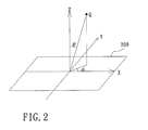
- Fig. 2 is a diagram that illustrates a coordinate system representing an end user viewing an LCD at a viewing position
- Figs. 3A, 38 and 3C are diagrams that illustrate a relationship between normalized luminance and gray scales of different viewing angles for red, green and blue light, respectively;
- Fig. 4 is a diagram that illustrates an example of a LCD display system with color shifting compensation for front and side viewing according to one embodiment of the present invention
- Figs. 5A and 5B are graphical views comparing luminance values of pixels in a conventional display system and a system according to the present invention
- Figs. 6A and 6B are diagrams showing examples of two adjacent images in a conventional display system
- Fig. 7 is a diagram showing an example of an image being displayed in a display system consistent with the present invention.
- Figs. 8A and 8B are diagrams showing examples of pixel matrices having a number of different pixel arrangements consistent with the present invention.
- Fig. 9 is a graphical representation of the display results of the relationship between blue normalized luminance and gray scales (Gamma Curve) at different viewing angles in one embodiment of a normally black LCD;
- Fig. 10 is a diagram that illustrates an example of a conventional LCD display system having an application specific integrated circuit ("ASIC"); and
- Fig. 11 is a diagram that illustrates an example of an LCD display system having an application specific integrated circuit ("ASIC") with color shifting compensation for front and side viewing according to one embodiment of the present invention.
- ASIC application specific integrated circuit
- the color displayed by a pixel in an image frame is divided into two colors having less color shifting being displayed in two subframes, or two colors having less color shifting being displayed in two adjacent pixels.
- Fig. 2 is a diagram that illustrates a coordinate system representing an end user viewing an LCD 200 at a viewing point Q.
- Figs. 3A, 3B and 3C are diagrams respectively illustrating the relationship between normalized transmittance (or luminance) and gray scales for different viewing angles for red, green and blue light, where gray scales for the pixels range from 0 to 255.
- the normalized transmittance (or luminance) value for a gray scale is the luminance of a front view corresponding to that gray scale divided by the maximum luminance for the front view, e.g., a gray scale value of 255 for a normally black display.
- the normalized transmittance (luminance) value for a gray scale of a side view is the luminance of the side view corresponding to that gray scale divided by the maximum luminance for the side view.
- the front view of the maximum luminance is different from the side view of the maximum luminance.
- an angle ⁇ is defined between the line from the center of LCD 200 to the viewing point Q and the Z axis
- an angle ⁇ is defined between the line projected from point Q onto LCD 200 and the X axis.
- ⁇ , ⁇ (0°, 0°)
- LCD 200 is being directly viewed from the front.
- ( ⁇ , ⁇ ) (0°, 45°) or (0°, 60°)
- LCD 200 is being viewed from the side at 45- and 60-degree angles, respectively.
- Fig. 4 illustrates an embodiment consistent with the present invention that employs adjusting the gray scale in the time domain and includes an LCD 400 display system with color shifting compensation for front and side viewing.
- LCD 400 comprises a plurality of pixels (a pixel being represented by, e.g., P(i, j), i and j being positive integers), data drivers 402, scan drivers 404, and a controller 406.
- Controller 406 further comprises an adjusted gray scale generator 407.
- One image frame is displayed in the LCD for each frame period.
- a frame period is divided into n subframes SFP 1 through SFP n , n being a positive integer.
- the original gray scales of pixels P(i, j) are GRO(i, j).
- a lookup table stored in adjusted gray scale generator 407 records all original gray scales (GR0) and at least one corresponding adjusted gray scale GR1 through GRn.
- Line d in Figs. 3A, 3B and 3C illustrates that Fig. 3C (the blue color) has the greatest difference between the front view and side view of normalized luminance. In view of this, the blue color may be adjusted first.
- Table 1 below shows an example of such a lookup table for the original and adjusted gray scales for blue color in a specific embodiment of a normally black, 20.1-inch, liquid crystal display (“LCD").
- the "Gray” represents the original gray scales for blue color
- "LUT 1" and “LUT 2" represent the adjusted gray scales for blue color GR1 and GR2, respectively.
- generator 407 (shown in Fig. 4) generates n adjusted gray scales from original gray scales GR0(i, j) for pixel P(i, j), including GR1(i, j), GR2(i, j) ... GRn(i, j).
- the n adjusted gray scales are input into corresponding data drivers 402 sequentially and accordingly displayed in n subframes.
- data drivers 402 drive pixels P(i, j) with n drive voltages corresponding to n adjusted gray scales.
- Original gray scales GR0(i, j) correspond to the original normalized luminance of front views ("L0(i, j)") and side views ("L0'(i, j)").
- adjusted normalized luminance for the front views and side views is determined from corresponding adjusted gray scales.
- the sum of the absolute value of the difference between the adjusted normalized luminance values for the front and side views should be less than the sum of the absolute value of the difference between the original normalized luminance values for the front and side views. Color shifting between the front and side views is advantageously minimized as a result.
- all of the adjusted normalized luminance values for the front views are generally the same as the original normalized luminance values for the front views, thereby assuring similarity between the original frame and the adjusted frame.
- Figs. 5A and 5B are graphical views comparing normalized transmittance values of pixels in a conventional display system and a system consistent with the present invention, respectively.
- Fig. 5A is a graphical view showing normalized transmittance values T(%) for pixels P(i, j) corresponding to original gray scales GR0 as the pixels are voltage driven, versus time, in a conventional display system.
- Fig. 5B is a graphical view showing the normalized transmittance values T(%) for pixels P(i, j) corresponding to adjusted gray scales GR1 through GRn as the pixels are voltage driven, versus time.
- a frame period (“FP") is divided into two subframe periods, namely SFP1 and SFP2.
- respective adjusted normalized luminance values L1(i, j) and L1'(i, j) for the front and side views, respectively, are determined from adjusted gray scales GR1(i, j).
- respective adjusted normalized luminance values L2(i, j) and L2'(i, j) for the front and side views, respectively, are determined from adjusted gray scales GR2(i, j).
- drive voltages corresponding to original gray scales GR0(i, j) are used to drive pixels P(i, j) for a frame period in a conventional display system, where the functions of normalized transmittance values T0(t) and T0'(t) respectively correspond to front and side views of pixels P(i, j).
- Original normalized luminance values L0(i, j) for the front view correspond to the integrated value of T0(t) within frame period FP.
- original normalized luminance values L0'(i, j) for the side view correspond to the integrated value of T0'(t) within frame period FP.
- drive voltages corresponding to adjusted gray scales GR1(i, j) are used to drive pixels P(i, j), where T1(t) and T1'(t) respectively represent the time function of normalized transmittance values for front and side views of pixels P(i, j).
- drive voltages corresponding to adjusted gray scales GR2(i, j) are used to drive pixels P(i, j) where T2(t) and T2'(t) respectively represent the time function of normalized transmittance values for front and side views of pixels P(i, j).
- Adjusted normalized luminance values L1 (i, j) for the front views correspond to the integrated value of T1(t) within subframe period SFP1 when drive voltages corresponding to adjusted gray scales GR1(i, j) are used to drive pixels P(i, j).
- Adjusted normalized luminance values L1'(i, j) for the side view correspond to the integrated value of T1'(t) within subframe period SFP1 when drive voltages corresponding to adjusted gray scales GR1(i, j) are used to drive pixels P(i, j).
- Adjusted normalized luminance values L2(i, j) for the front view correspond to the integrated value of T2(t) within subframe period SFP2 when drive voltages corresponding to adjusted gray scales GR2(i, j) are used to drive pixels P(i, j).
- Adjusted normalized luminance values L2'(i, j) for the side view correspond to the integrated value of T2'(t) within subframe period SFP2 when drive voltages corresponding to adjusted gray scales GR2(i, j) are used to drive pixels P(i, j).
- adjusted gray scales GR1(i, j) and GR2(i, j) corresponding to the sum of normalized luminance values L1(i, j) and L2(i, j) for the front views are generally the same as normalized original luminance values L0(i, j) for the front views.
- the luminance for the pixels is attributed to the cumulative effect of luminance values for adjusted gray scales GR1 (i, j) and GR2(i, j) respectively corresponding to subframe periods SFP1 and SFP2, which approximates the luminance of original gray scales GR0 corresponding to pixels within a frame period FP in a conventional display system.
- each of SFP1 and SFP2 is advantageously one half of frame period FP.
- original gray scales GR0(i, j) are advantageously between adjusted gray scales GR1(i, j) and GR2(i, j).
- adjusted gray scales GR1(i, j) are greater than GR2(i, j).
- the absolute value of the difference of the normalized luminance value between the front and side (from 60 degrees) views for gray scale 0 is very small, which is well suited to serve as GR2(i, j).
- Image display is properly ascertained by dynamically and continuously adjusting GR1(i, j) and GR2(i, j) within a frame period FP to achieve optimal luminance.
- GR1(i, j) and GR2(i, j) can be (190, 0) or (0, 190), respectively.
- original gray scales GR0(i, j) are fixed and corresponding normalized luminance values L0(i, j) are measured.
- the original frame period is divided into two equivalent subframe periods. Since the change between front and side views for gray scale 0 is the smallest, and for reducing response time for driving liquid crystal elements, gray scale 0 is selected to be GR2(i, j). Since the characteristics for driving liquid crystal elements are not rectangular waves, adjustment is needed for GR1(i, j) and GR2(i, j) so that the sum of normalized luminance values L1(i, j) and L2(i, j) is generally the same as original normalized luminance values L0(i, j).
- the cumulative effect of the differences between normalized luminance values for the front and side views corresponding to gray scales GR1(i, j) in SFP1 and normalized luminance values for the front and side views corresponding to gray scales GR2(i, j) in SFP2 is less, compared with the difference between normalized luminance values for the front and side views corresponding to gray scales GR0(i, j) in a frame period FP in a conventional system.
- GR1(i, j) and GR2(i, j) accordingly obtained for all gray scales are then used to form the lookup table.
- a further embodiment consistent with the present invention is implemented in the space domain for changing the gray scales. Color shifting with respect to the front and side views is compensated by displaying an image within a single frame period ("FP").
- the display system includes a liquid crystal display (“LCD") further comprising a display panel, a plurality of data drivers, a plurality of scan drivers and a controller.
- the panel further comprises a plurality of pixels
- the controller further includes an adjusted gray scale generator.
- the adjusted gray scale generator For two pixels Pa and Pb, the adjusted gray scale generator generates adjusted gray scales GRa1 and GRb1 for original gray scales GRa0 and GRb0 for the pixels Pa and Pb, respectively.
- GRa0 and GRb0 respectively correspond to the original normalized luminance values for the front and side views (La and La'), and the original normalized luminance values for the front and side views (Lb and Lb').
- data drivers respectively drive the two pixels Pa and Pb with first and second drive voltages corresponding to adjusted gray scales GRa1 and GRb1.
- pixel Pa is driven with the first drive voltage
- Pa includes adjusted normalized luminance values Lc and Lc' for the front and side views, respectively.
- pixel Pb is driven with the second drive voltage
- Pb includes adjusted normalized luminance values Ld and Ld' for the front and side views, respectively.
- the adjusted gray scale generator comprises a lookup table, from which adjusted gray scales GRa1 and GRb1 are generated.
- the lookup table records original gray scales GRa0 and GRb0, and corresponding adjusted gray scales GRa1 and GRb1.
- pixels Pa and Pb are adjacent to each other and have the same color.
- Original gray scales GRa0 and GRb0 are between adjusted gray scales GRa1 and GRb1.
- Adjusted normalized luminance values for the front and side views (Lc and Ld, respectively) are generally the same as the sum of original normalized luminance values for the front and side views La and Lb.
- Figs. 6A and 68 are diagrams showing examples of two adjacent images M and M+1 in a conventional display system.
- Fig. 7 is a diagram showing an example of an image being displayed in a display system consistent with the present invention.
- Red, green and blue pixels are respectively represented by letters R, G and B.
- Original gray scales for adjacent pixels are generally close, e.g., blue pixels B11 and B21 having the same original gray scale at 128.
- Adjusted gray scales GRa1 at 174 and GRb1 at 0 are selected when blue pixels B11 and B21 have the same original gray scale 128.
- gray scales for blue pixels B11 and B21 are 174 and 0, respectively, consistent with the present invention.
- gray scales for B11 and B21 are 0 and 174, respectively.
- pixels having different colors have relatively large gaps therebetween.
- pixel matrices can have a number of different pixel arrangements.
- one embodiment of the present invention provides a display device comprising a plurality of pixels in rows and columns having a first color, a second color and a third color, wherein two adjacent pixels in one of the rows have the same color.
- the present invention provides a display device comprising a plurality of pixels in rows and columns having a first color, a second color and a third color, wherein two adjacent pixels in one of the rows have the same color.
- Figs. 8A and 8B are diagrams showing examples of pixel matrices having a number of different pixel arrangements.
- two adjacent pixels in a row can also be the same color, as shown in Fig. 8A, such as a row of pixels GRBBRGGRB.
- There can be different arrangements of mixed order for every row such as the order of the two adjacent rows GRBBRGGRB and BRGGRBBRG.
- pixels G and B have the same adjacent pixel, so the gap between the two single-color pixels (G and B) is advantageously reduced.
- the order of the pixels can be arranged so that two pixels are diagonally adjacent one another in an LCD panel, as shown in Fig. 8B. Referring to Fig.
- a pair of red pixels R and a pair of blue pixels B are horizontally arranged, whereas a pair of green pixels G is located above or below the pair of red pixels R and the pair of blue pixels B. Green pixels G is further located in a mixed manner below red pixels R and blue pixels B, so pixels of the same color are adjacent along the diagonal lines in the LCD panel. Gaps between the single-color pixels are advantageously reduced as a result, as shown in Figs. 8A and 8B, which is conducive to optimizing the resolution for the pixels.
- Figs. 10 and 11 are diagrams illustrating examples of an LCD display system having an application specific integrated circuit ("ASIC"), respectively without color shifting compensation (Fig. 10), and with color shifting compensation (Fig. 11) for front and side viewing according to one embodiment of the present invention.
- ASIC application specific integrated circuit
- an LCD panel 100 comprises 1024 red, green and blue (“RGB") data lines, namely, 1024 x 3 data lines, and 768 scan lines, similar to the LCD panel shown in Fig. 1.
- the data lines and scan lines are respectively driven by a plurality of data drivers 102 and scan drivers 104.
- a power supply 103 supplies power to data drivers 102 and scan drivers 104.
- An ASIC 101 includes timing controller 106 that outputs a data control signal to data drivers 102, which accordingly receive and process the pixel data from controller 106. After processing the received pixel data, each of data drivers 102 outputs corresponding voltages for driving 384 data lines in LCD panel 100.
- Scan drivers 104 at the control of a scan control signal from controller 106, respectively output scan signals and control 256 scan lines. After scanning all of the scan lines, all of the pixels have been driven for completing the display of an image frame.
- Fig. 11 is a diagram that illustrates an example of an LCD display system having an application specific integrated circuit ("ASIC 411") with color shifting compensation for front and side viewing according to one embodiment of the present invention.
- LCD 400 comprises a plurality of pixels (a pixel being represented by, e.g., P(i, j), i and j being positive integers), data drivers 402, scan drivers 404, and a timing controller 406, similar to the LCD panel shown in Fig. 4.
- One image is displayed in the LCD for each frame period.
- a frame period is divided into n subframes SFP 1 through SFP n , n being a positive integer.
- the original gray scales of pixels P(i, j) are GR0(i, j).
- a lookup table LUT1 records the original gray scales (GR0) and the corresponding adjusted gray scales GR1.
- a lookup table LUT2 records the original gray scales (GR0) and corresponding adjusted gray scales GR2.
- a power supply 403 supplies power to data drivers 402 and scan drivers 404.
- Timing controller 406 in ASIC 401 outputs a data control signal to data drivers 402, which accordingly receive and process the pixel data from controller 406.
- ASIC 411 further includes a data selector 405, LUT 1 and LUT 2, an interface 408 provided between LUT 2 and a memory 409 (which is an EEPROM).
- embodiments of display devices and methods consistent with the present invention for compensating color shifting between front and side views of images can advantageously minimize the effects of color shifting and optimize image quality of the display device.
- One embodiment is advantageously implemented in a multi-domain vertically aligned LCD.
- embodiments consistent with the present invention can be implemented in an LCD for all of its pixels, or specifically implemented to particular pixels, to reduce the adverse effects of color shifting.
Landscapes
- Engineering & Computer Science (AREA)
- Physics & Mathematics (AREA)
- Computer Hardware Design (AREA)
- General Physics & Mathematics (AREA)
- Theoretical Computer Science (AREA)
- Chemical & Material Sciences (AREA)
- Crystallography & Structural Chemistry (AREA)
- Control Of Indicators Other Than Cathode Ray Tubes (AREA)
- Liquid Crystal Display Device Control (AREA)
Applications Claiming Priority (2)
| Application Number | Priority Date | Filing Date | Title |
|---|---|---|---|
| CN04101640 | 2004-01-07 | ||
| CN04101640 | 2004-01-07 |
Publications (2)
| Publication Number | Publication Date |
|---|---|
| EP1553553A2 true EP1553553A2 (fr) | 2005-07-13 |
| EP1553553A3 EP1553553A3 (fr) | 2008-07-30 |
Family
ID=34580549
Family Applications (1)
| Application Number | Title | Priority Date | Filing Date |
|---|---|---|---|
| EP04019705A Ceased EP1553553A3 (fr) | 2004-01-07 | 2004-08-19 | Circuit de commande pour compensation de l'angle de vue pour un dispositif d'affichage à cristaux liquides |
Country Status (1)
| Country | Link |
|---|---|
| EP (1) | EP1553553A3 (fr) |
Cited By (8)
| Publication number | Priority date | Publication date | Assignee | Title |
|---|---|---|---|---|
| EP1564714A3 (fr) * | 2004-01-21 | 2007-11-21 | Sharp Kabushiki Kaisha | Dispositif d'affichage, moniteur à cristaux liquides, téléviseur à cristaux liquides, et méthode d'affichage |
| EP2101312A1 (fr) * | 2006-11-28 | 2009-09-16 | Sharp Kabushiki Kaisha | Circuit de conversion de signaux et dispositif d'affichage à cristaux liquides à couleurs primaires multiples équipé du circuit |
| US8508449B2 (en) | 2008-12-18 | 2013-08-13 | Sharp Corporation | Adaptive image processing method and apparatus for reduced colour shift in LCDs |
| WO2016045251A1 (fr) * | 2014-09-26 | 2016-03-31 | 京东方科技集团股份有限公司 | Procédé et dispositif d'affichage d'image |
| WO2019041398A1 (fr) * | 2017-08-28 | 2019-03-07 | 惠科股份有限公司 | Procédé de calcul de compensation d'angle de visée de dispositif d'affichage, structure de compensation d'angle de visée et dispositif d'affichage |
| CN114613314A (zh) * | 2022-05-10 | 2022-06-10 | 深圳市时代华影科技股份有限公司 | 画面显示控制方法、装置、设备与介质 |
| WO2022213699A1 (fr) * | 2021-04-07 | 2022-10-13 | 深圳Tcl数字技术有限公司 | Procédé et appareil d'affichage d'image, dispositif d'affichage et support de stockage |
| CN115083365B (zh) * | 2022-07-07 | 2023-06-27 | Tcl华星光电技术有限公司 | 画面显示方法和画面显示装置 |
Citations (1)
| Publication number | Priority date | Publication date | Assignee | Title |
|---|---|---|---|---|
| US20030146893A1 (en) | 2002-01-30 | 2003-08-07 | Daiichi Sawabe | Liquid crystal display device |
Family Cites Families (10)
| Publication number | Priority date | Publication date | Assignee | Title |
|---|---|---|---|---|
| JPS6037526A (ja) * | 1983-08-10 | 1985-02-26 | Mitsubishi Electric Corp | 液晶表示素子の駆動方式 |
| JP3202450B2 (ja) * | 1993-10-20 | 2001-08-27 | 日本電気株式会社 | 液晶表示装置 |
| US6801220B2 (en) * | 2001-01-26 | 2004-10-05 | International Business Machines Corporation | Method and apparatus for adjusting subpixel intensity values based upon luminance characteristics of the subpixels for improved viewing angle characteristics of liquid crystal displays |
| KR100870487B1 (ko) * | 2001-07-04 | 2008-11-26 | 엘지디스플레이 주식회사 | 광시야각을 위한 액정디스플레이의 구동 방법 및 장치 |
| KR100806901B1 (ko) * | 2001-09-03 | 2008-02-22 | 삼성전자주식회사 | 광시야각 모드용 액정 표시 장치와 이의 구동 방법 |
| US7417648B2 (en) * | 2002-01-07 | 2008-08-26 | Samsung Electronics Co. Ltd., | Color flat panel display sub-pixel arrangements and layouts for sub-pixel rendering with split blue sub-pixels |
| TWI227340B (en) * | 2002-02-25 | 2005-02-01 | Himax Tech Inc | Color filter and liquid crystal display |
| KR100884993B1 (ko) * | 2002-04-20 | 2009-02-20 | 엘지디스플레이 주식회사 | 액정표시장치 및 그 구동방법 |
| JP4248306B2 (ja) * | 2002-06-17 | 2009-04-02 | シャープ株式会社 | 液晶表示装置 |
| JP3760903B2 (ja) * | 2002-08-22 | 2006-03-29 | セイコーエプソン株式会社 | 画像表示装置 |
-
2004
- 2004-08-19 EP EP04019705A patent/EP1553553A3/fr not_active Ceased
Patent Citations (1)
| Publication number | Priority date | Publication date | Assignee | Title |
|---|---|---|---|---|
| US20030146893A1 (en) | 2002-01-30 | 2003-08-07 | Daiichi Sawabe | Liquid crystal display device |
Cited By (16)
| Publication number | Priority date | Publication date | Assignee | Title |
|---|---|---|---|---|
| EP1564714A3 (fr) * | 2004-01-21 | 2007-11-21 | Sharp Kabushiki Kaisha | Dispositif d'affichage, moniteur à cristaux liquides, téléviseur à cristaux liquides, et méthode d'affichage |
| US7932915B2 (en) | 2004-01-21 | 2011-04-26 | Sharp Kabushiki Kaisha | Display device, liquid crystal monitor, liquid crystal television receiver, and display method |
| US8520036B2 (en) | 2004-01-21 | 2013-08-27 | Sharp Kabushiki Kaisha | Display device, liquid crystal monitor, liquid crystal television receiver, and display method |
| EP2101312A1 (fr) * | 2006-11-28 | 2009-09-16 | Sharp Kabushiki Kaisha | Circuit de conversion de signaux et dispositif d'affichage à cristaux liquides à couleurs primaires multiples équipé du circuit |
| EP2101312A4 (fr) * | 2006-11-28 | 2010-10-27 | Sharp Kk | Circuit de conversion de signaux et dispositif d'affichage à cristaux liquides à couleurs primaires multiples équipé du circuit |
| US8294739B2 (en) | 2006-11-28 | 2012-10-23 | Sharp Kabushiki Kaisha | Signal conversion circuit and multiple primary color liquid crystal display device with the circuit |
| US8654116B2 (en) | 2006-11-28 | 2014-02-18 | Sharp Kabushiki Kaisha | Signal conversion circuit and multiple primary color liquid crystal display device with the circuit |
| US8508449B2 (en) | 2008-12-18 | 2013-08-13 | Sharp Corporation | Adaptive image processing method and apparatus for reduced colour shift in LCDs |
| WO2016045251A1 (fr) * | 2014-09-26 | 2016-03-31 | 京东方科技集团股份有限公司 | Procédé et dispositif d'affichage d'image |
| US10467939B2 (en) | 2014-09-26 | 2019-11-05 | Boe Technology Group Co., Ltd. | Method for displaying image and display device |
| WO2019041398A1 (fr) * | 2017-08-28 | 2019-03-07 | 惠科股份有限公司 | Procédé de calcul de compensation d'angle de visée de dispositif d'affichage, structure de compensation d'angle de visée et dispositif d'affichage |
| US10657907B2 (en) | 2017-08-28 | 2020-05-19 | HKC Corporation Limited | Calculation method for viewing-angle compensation of display device, viewing-angle compensation structure, and display device |
| WO2022213699A1 (fr) * | 2021-04-07 | 2022-10-13 | 深圳Tcl数字技术有限公司 | Procédé et appareil d'affichage d'image, dispositif d'affichage et support de stockage |
| CN114613314A (zh) * | 2022-05-10 | 2022-06-10 | 深圳市时代华影科技股份有限公司 | 画面显示控制方法、装置、设备与介质 |
| WO2023217199A1 (fr) * | 2022-05-10 | 2023-11-16 | 深圳市时代华影科技股份有限公司 | Procédé, appareil et dispositif de commande d'affichage d'image, et support |
| CN115083365B (zh) * | 2022-07-07 | 2023-06-27 | Tcl华星光电技术有限公司 | 画面显示方法和画面显示装置 |
Also Published As
| Publication number | Publication date |
|---|---|
| EP1553553A3 (fr) | 2008-07-30 |
Similar Documents
| Publication | Publication Date | Title |
|---|---|---|
| US7843414B2 (en) | Liquid crystal display driver and method thereof | |
| KR100518286B1 (ko) | 액정 표시 장치 | |
| JP5863925B2 (ja) | 制御装置及び制御方法 | |
| TWI578303B (zh) | 顯示面板及顯示面板的驅動方法 | |
| TWI476753B (zh) | 處理用於顯示於包含多原色圖像顯示面板之顯示裝置之圖像資料之方法 | |
| KR100750929B1 (ko) | 색 보정 기능을 갖는 액정 표시 장치 및 이의 구동 장치및 그 방법 | |
| US7460115B2 (en) | Display apparatus using subpixels with high light utilization | |
| US7619641B2 (en) | Color display | |
| US7688295B2 (en) | Drive system and method for a color display | |
| US20040174375A1 (en) | Sub-pixel rendering system and method for improved display viewing angles | |
| US20050146492A1 (en) | Field-sequential color display unit and display method | |
| US8243105B2 (en) | Display device, display device adjustment method, image display monitor, and television receiver | |
| US20060221030A1 (en) | Displaying method and image display device | |
| US20070052721A1 (en) | Systems and methods for temporal subpixel rendering of image data | |
| WO2013022007A1 (fr) | Dispositif d'affichage | |
| KR20020083489A (ko) | 화상처리회로, 화상표시장치, 및 화상처리방법 | |
| US20210217373A1 (en) | Method for driving pixel matrix and display device | |
| CN100454086C (zh) | 液晶显示器及驱动方法 | |
| EP1553553A2 (fr) | Circuit de commande pour compensation de l'angle de vue pour un dispositif d'affichage à cristaux liquides | |
| JPH0990910A (ja) | 液晶表示装置の駆動方法および液晶表示装置 | |
| US20200342823A1 (en) | Method for driving pixel matrix and display device | |
| KR20060111148A (ko) | 표시 장치의 구동 장치 및 구동 방법 | |
| US7154465B2 (en) | Multi-line selection driving method for a super-twisted nematic liquid crystal display having low-power consumption | |
| JP2003228337A (ja) | モノクロ・フラットパネル・ディスプレイ装置 | |
| CN115083365B (zh) | 画面显示方法和画面显示装置 |
Legal Events
| Date | Code | Title | Description |
|---|---|---|---|
| PUAI | Public reference made under article 153(3) epc to a published international application that has entered the european phase |
Free format text: ORIGINAL CODE: 0009012 |
|
| AK | Designated contracting states |
Kind code of ref document: A2 Designated state(s): AT BE BG CH CY CZ DE DK EE ES FI FR GB GR HU IE IT LI LU MC NL PL PT RO SE SI SK TR |
|
| AX | Request for extension of the european patent |
Extension state: AL HR LT LV MK |
|
| RAP3 | Party data changed (applicant data changed or rights of an application transferred) |
Owner name: CHI MEI OPTOELECTRONICS CORPORATION |
|
| RIN1 | Information on inventor provided before grant (corrected) |
Inventor name: LI, WANG-YANGC/O CHI MEI OPTOELECTRONICS CORP. Inventor name: SHIH, MING-CHIAC/O CHI MEI OPTOELECTRONICS CORP. Inventor name: HSU, YING-HAOC/O CHI MEI OPTOELECTRONICS CORP. |
|
| PUAL | Search report despatched |
Free format text: ORIGINAL CODE: 0009013 |
|
| AK | Designated contracting states |
Kind code of ref document: A3 Designated state(s): AT BE BG CH CY CZ DE DK EE ES FI FR GB GR HU IE IT LI LU MC NL PL PT RO SE SI SK TR |
|
| AX | Request for extension of the european patent |
Extension state: AL HR LT LV MK |
|
| 17P | Request for examination filed |
Effective date: 20090128 |
|
| AKX | Designation fees paid |
Designated state(s): DE FR GB IT |
|
| 17Q | First examination report despatched |
Effective date: 20100621 |
|
| RAP1 | Party data changed (applicant data changed or rights of an application transferred) |
Owner name: CHIMEI INNOLUX CORPORATION |
|
| STAA | Information on the status of an ep patent application or granted ep patent |
Free format text: STATUS: THE APPLICATION HAS BEEN REFUSED |
|
| 18R | Application refused |
Effective date: 20140921 |