EP1551064A2 - Light emitting device and manufacturing method thereof. - Google Patents
Light emitting device and manufacturing method thereof. Download PDFInfo
- Publication number
- EP1551064A2 EP1551064A2 EP04293146A EP04293146A EP1551064A2 EP 1551064 A2 EP1551064 A2 EP 1551064A2 EP 04293146 A EP04293146 A EP 04293146A EP 04293146 A EP04293146 A EP 04293146A EP 1551064 A2 EP1551064 A2 EP 1551064A2
- Authority
- EP
- European Patent Office
- Prior art keywords
- layer
- contact layer
- trench portion
- substrate
- current spreading
- Prior art date
- Legal status (The legal status is an assumption and is not a legal conclusion. Google has not performed a legal analysis and makes no representation as to the accuracy of the status listed.)
- Withdrawn
Links
- 238000004519 manufacturing process Methods 0.000 title claims abstract description 20
- 239000000758 substrate Substances 0.000 claims abstract description 50
- 238000000034 method Methods 0.000 claims description 51
- 230000007480 spreading Effects 0.000 claims description 40
- 238000003892 spreading Methods 0.000 claims description 40
- 230000008569 process Effects 0.000 claims description 16
- 239000004065 semiconductor Substances 0.000 claims description 14
- 238000005530 etching Methods 0.000 claims description 12
- 238000004943 liquid phase epitaxy Methods 0.000 claims description 10
- 238000005229 chemical vapour deposition Methods 0.000 claims description 7
- 238000001312 dry etching Methods 0.000 claims description 7
- 239000000463 material Substances 0.000 claims description 6
- 229910052751 metal Inorganic materials 0.000 claims description 6
- 239000002184 metal Substances 0.000 claims description 6
- 238000001451 molecular beam epitaxy Methods 0.000 claims description 5
- 238000001039 wet etching Methods 0.000 claims description 5
- 238000000059 patterning Methods 0.000 claims description 4
- 239000012780 transparent material Substances 0.000 claims description 4
- 229910001218 Gallium arsenide Inorganic materials 0.000 claims description 3
- 229910052594 sapphire Inorganic materials 0.000 claims description 3
- 239000010980 sapphire Substances 0.000 claims description 3
- JBRZTFJDHDCESZ-UHFFFAOYSA-N AsGa Chemical compound [As]#[Ga] JBRZTFJDHDCESZ-UHFFFAOYSA-N 0.000 claims description 2
- 229910002601 GaN Inorganic materials 0.000 claims description 2
- JMASRVWKEDWRBT-UHFFFAOYSA-N Gallium nitride Chemical compound [Ga]#N JMASRVWKEDWRBT-UHFFFAOYSA-N 0.000 claims description 2
- XUIMIQQOPSSXEZ-UHFFFAOYSA-N Silicon Chemical compound [Si] XUIMIQQOPSSXEZ-UHFFFAOYSA-N 0.000 claims description 2
- 238000012545 processing Methods 0.000 claims description 2
- 229910052710 silicon Inorganic materials 0.000 claims description 2
- 239000010703 silicon Substances 0.000 claims description 2
- HBMJWWWQQXIZIP-UHFFFAOYSA-N silicon carbide Chemical compound [Si+]#[C-] HBMJWWWQQXIZIP-UHFFFAOYSA-N 0.000 claims description 2
- 229910010271 silicon carbide Inorganic materials 0.000 claims description 2
- 230000001965 increasing effect Effects 0.000 abstract description 8
- 230000003287 optical effect Effects 0.000 description 4
- 230000002708 enhancing effect Effects 0.000 description 3
- 238000001259 photo etching Methods 0.000 description 3
- 230000003466 anti-cipated effect Effects 0.000 description 2
- 239000003086 colorant Substances 0.000 description 2
- 238000000151 deposition Methods 0.000 description 2
- 239000010409 thin film Substances 0.000 description 2
- 238000004891 communication Methods 0.000 description 1
- 150000001875 compounds Chemical class 0.000 description 1
- 230000008021 deposition Effects 0.000 description 1
- 238000010438 heat treatment Methods 0.000 description 1
- AMGQUBHHOARCQH-UHFFFAOYSA-N indium;oxotin Chemical compound [In].[Sn]=O AMGQUBHHOARCQH-UHFFFAOYSA-N 0.000 description 1
- 238000012986 modification Methods 0.000 description 1
- 230000004048 modification Effects 0.000 description 1
- 238000011160 research Methods 0.000 description 1
- 230000007704 transition Effects 0.000 description 1
Images



Classifications
-
- H—ELECTRICITY
- H10—SEMICONDUCTOR DEVICES; ELECTRIC SOLID-STATE DEVICES NOT OTHERWISE PROVIDED FOR
- H10H—INORGANIC LIGHT-EMITTING SEMICONDUCTOR DEVICES HAVING POTENTIAL BARRIERS
- H10H20/00—Individual inorganic light-emitting semiconductor devices having potential barriers, e.g. light-emitting diodes [LED]
- H10H20/80—Constructional details
- H10H20/81—Bodies
- H10H20/819—Bodies characterised by their shape, e.g. curved or truncated substrates
- H10H20/821—Bodies characterised by their shape, e.g. curved or truncated substrates of the light-emitting regions, e.g. non-planar junctions
Definitions
- the present invention relates to a light emitting device and a manufacturing method thereof, and more particularly, to a light emitting device capable of enhancing a light emitting efficiency by increasing a light emitting area of an active layer deposited on an upper surface of a substrate and a manufacturing method thereof.
- a light emitting device currently being widely used can be largely divided into a laser diode (LD) and a light emitting diode (LED).
- LD laser diode
- LED light emitting diode
- the LD is being widely used as an optical source in an optical communication field. Recently, the LD is being used in an optical media field such as not only a compact disc (CD) reproducing apparatus and a compact disc recording-reproducing apparatus (CD-RW) but also a DVD reproducing apparatus, a laser disc (LD) reproducing apparatus, a minimum disc (MD) reproducing apparatus, etc.
- CD compact disc
- CD-RW compact disc recording-reproducing apparatus
- DVD reproducing apparatus a laser disc (LD) reproducing apparatus
- MD minimum disc
- the LED is used as a general display device, and is also used as a backlight source of a lighting device or an LCD display device.
- the LED can be driven with a comparatively low voltage. Also, the LED has a low heating value due to a high energy efficiency and has a long lifespan. According to this, technique concerning about the LED is being anticipated as a major technique to substitute most of lighting devices currently being used such as a fluorescent lamp, an incandescent lamp, a traffic light, a light for a car, etc.
- a research for using the LED as a backlight source of a display device by arranging as an array is being actively performed.
- the LED is anticipated as an optical source of backlight to substitute a cold cathode fluorescent lamp (CCFL) used in a thin film transistor (TFT)-LCD.
- CCFL cold cathode fluorescent lamp
- TFT thin film transistor
- Light emitting devices using a group III ⁇ V material of a direct transition type compound semiconductor such as an LD or an LED can implement various colors such as green, blue, and ultraviolet rays as a thin film growing technique and a device material are developed. Also, since white ray having a good efficiency can be implemented by using fluorescent materials or by combining colors, the light emitting device can be variously used. In order for the light emitting device to be variously used, a low driving voltage and light of a high brightness are required.
- FIG. 1 is a longitudinal section view showing a light emitting device in accordance with the conventional art.
- the conventional light emitting device 10 is formed as a buffer layer 12, an n-contact layer 13, an active layer 14, and a p-contact layer 15 are sequentially deposited on an upper surface of a substrate 11 such as sapphire n-GaAs, etc. by a chemical vapor deposition (CVD) method.
- CVD chemical vapor deposition
- a photosensitive mask (not shown) is patterned on the p-contact layer 15. Then, an exposure and an etching are performed until a part 13' of the n-contact layer 13 is exposed by a photo etching process and a wet etching process (or a dry etching process), and then the photosensitive mask is removed.
- a current spreading layer 16 is deposited on the p-contact layer 15, and a p-electrode 17 electrically connected to the p-contact layer 15 and the current spreading layer 16 is formed on the current spreading layer 16. Then, an n-electrode 18 is formed on the exposed part 13' of the n-contact layer 13.
- the buffer layer, the n-contact layer, and the active layer are sequentially deposition on the flat upper surface of the substrate, there is a limitation in forming a light emitting area of the active layer that is the most important layer to determine a light emitting efficiency of a light emitting device to be large.
- an object of the present invention is to provide a light emitting device capable of reducing a production cost and capable of enhancing a light emitting efficiency by increasing a light emitting area of an active layer by forming a trench portion on a substrate of the light emitting device and by sequentially depositing a buffer layer, an n-contact layer, and an active layer on the trench portion, and a manufacturing method thereof.
- a light emitting device comprising: a substrate having a trench portion on an upper surface thereof; a buffer layer formed on the trench portion of the substrate; an n-contact layer formed on an upper surface of the buffer layer; an active layer formed at one side of an upper surface of the n-contact layer; a p-contact layer formed on an upper surface of the active layer; a current spreading layer formed on an upper surface of the p-contact layer; a p-electrode formed on an upper surface of the current spreading layer so as to be electrically connected to the active layer and the p-contact layer; and an n-electrode formed at another side of the upper surface of the n-contact layer so as to be electrically connected to the n-contact layer.
- a manufacturing method of a light emitting device comprising the steps of: forming a trench portion on an upper surface of a substrate; forming a buffer layer, an n-contact layer, an active layer, a p-contact layer, and a current spreading layer on the upper surface of the substrate where the trench portion is formed; partially removing the active layer, the p-contact layer, and the current spreading layer so that the n-contact layer can be partially exposed; forming a p-electrode on an upper surface of the current spreading layer so as to be electrically connected to the active layer and the p-contact layer; and forming an n-electrode on an upper surface of the exposed n-contact layer so as to be electrically connected to the n-contact layer.
- FIG. 2 is a perspective view showing a light emitting device according to first embodiment of the present invention.
- a light emitting area of an active layer 140 is increased by forming a trench portion 111 having a section of a 'V' shape on an upper surface of a substrate 110 by a half cut dicing method and then by forming a semiconductor layer 190 on an upper surface of the trench portion 111, and thereby a light emitting efficiency is enhanced.
- the light emitting device 100 comprises: a substrate 110 having a trench portion 111 on an upper surface thereof; a buffer layer 120 formed on the trench portion 111 of the substrate 110; an n-contact layer 130 formed on an upper surface of the buffer layer 120; an active layer 140 formed at one side of an upper surface of the n-contact layer 130; a p-contact layer 150 formed on an upper surface of the active layer 140; a current spreading layer 160 formed on an upper surface of the p-contact layer 150; a p-electrode 170 formed on an upper surface of the current spreading layer 160 so as to be electrically connected to the active layer 140 and the p-contact layer 150; and an n-electrode 180 formed at another side of the upper surface of the n-contact layer 130 so as to be electrically connected to the n-contact layer 130.
- the buffer layer 120 and the n-contact layer 130 of the semiconductor layer 190 are formed by a metal organic chemical vapor deposition (MOCVD) method, a molecular beam epitaxy (MBE) method, or a liquid phase epitaxy (LPE) method.
- MOCVD metal organic chemical vapor deposition
- MBE molecular beam epitaxy
- LPE liquid phase epitaxy
- the trench portion 111 can be formed on the entire upper surface of the substrate 110, and can be formed only at a part where a MESA, a light emission region, is formed.
- the current spreading layer 160 is formed of a transparent material having a high light transmissivity. According to this, light emitted from the active layer 140 passes through the current spreading layer 160 and is emitted upwardly.
- the current spreading layer can be formed of a metal electrode of a reflective material. At this time, light emitted from the active layer is emitted towards a lower direction of the substrate.
- the current spreading layer 160 is formed of Ni/Au or ITO (Indium Tin Oxide).
- the substrate 110 is formed of sapphire, gallium arsenide, silicon, silicon carbide, or gallium nitride.
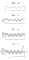
- FIGs. 3 to 8 are views showing a manufacturing method of the light emitting device according to first embodiment of the present invention.
- a manufacturing method of a light emitting device comprises the steps of: forming a trench portion 111 at a part of an upper surface of a substrate 110 by a half cut dicing method; forming a buffer layer 120, an n-contact layer 130, an active layer 140, a p-contact layer 150, and a current spreading layer 160 on the upper surface of the substrate 110 where the trench portion 111 is formed; partially removing the active layer 140, the p-contact layer 150, and the current spreading layer 160 so that the n-contact layer 130 can be partially exposed; forming a p-electrode 170 on an upper surface of the current spreading layer 160 so as to be electrically connected to the active layer 140 and the p-contact layer 150; and forming an n-electrode 180 on an upper surface of the exposed n-contact layer so as to be electrically connected to the n-contact layer 150.
- the trench portion 111 is formed on an upper surface of the substrate 110 by moving a dicing blade B used in a half cut dicing process in a zigzag direction on the upper surface of the substrate 110, a mother substrate.
- the trench portion 111 can be formed on the entire upper surface of the substrate 110, and can be formed only at a part where a MESA, a light emission region, is formed.
- a shape of the trench portion 111 is determined by a shape of the dicing blade B. For example, when the dicing blade has a 'V' shape, the trench portion has a 'V' shape, and when the dicing blade has a 'U' shape, the trench portion has a 'U' shape.
- the buffer layer 120, the n-contact layer 130, the active layer 140, the p-contact layer 150, and the current spreading layer 160 are formed on the entire upper surface of the substrate 110 where the trench portion 111 is formed.
- the semiconductor layer 190 is curvedly formed according to the shape of the trench portion 111. Therefore, a light emitting area of the active layer 140 of the semiconductor layer 190 becomes relatively large thereby to enhance a light emitting efficiency.
- the buffer layer 120 and the n-contact layer 130 are formed by a metal organic chemical vapor deposition (MOCVD) method, a molecular beam epitaxy (MBE) method, or a liquid phase epitaxy (LPE) method.
- MOCVD metal organic chemical vapor deposition
- MBE molecular beam epitaxy
- LPE liquid phase epitaxy
- a photosensitive mask (not shown) is patterned on the p-contact layer 150. Then, an exposure and an etching are performed until a part 130' of the n-contact layer 130 is exposed by a photo etching process and a wet etching process (or a dry etching process), and then the photosensitive mask is removed.
- the p-electrode 170 is formed on an upper surface of the current spreading layer 160 so as to be electrically connected to the active layer 140 and the p-contact layer 150
- the n-electrode 180 is formed on an upper surface of the exposed n-contact layer 130', one part 130' of the n-contact layer 130, thereby completing the light emitting device 100.
- the p-electrode 170 has the same potential as the current spreading layer 160 and the p-contact layer 150
- the n-electrode 180 has the same potential as the n-contact layer 130.
- FIG. 9 is a perspective view showing a light emitting device according to a second embodiment of the present invention.
- a light emitting area of an active layer 240 is increased by forming a trench portion 211 having a section of a 'V' shape on an upper surface of a substrate 210 by an etching process by an etching mask 203 and then by forming a semiconductor layer 290 on an upper surface of the trench portion 211, and thereby a light emitting efficiency is enhanced.
- the light emitting device 200 comprises: a substrate 210 having a trench portion 211 at a part of an upper surface thereof; a buffer layer 220 formed on the trench portion 211 of the substrate 210; an n-contact layer 230 formed on an upper surface of the buffer layer 220; an active layer 240 formed at one side of an upper surface of the n-contact layer 230; a p-contact layer 250 formed on an upper surface of the active layer 240; a current spreading layer 260 formed on an upper surface of the p-contact layer 250; a p-electrode 270 formed on an upper surface of the current spreading layer 260 so as to be electrically connected to the active layer 240 and the p-contact layer 250; and an n-electrode 280 formed at another side of the upper surface of the n-contact layer 230 so as to be electrically connected to the n-contact layer 230.
- the buffer layer 220 and the n-contact layer 230 of the semiconductor layer 290 are formed by a metal organic chemical vapor deposition (MOCVD) method, a molecular beam epitaxy (MBE) method, or a liquid phase epitaxy (LPE) method.
- MOCVD metal organic chemical vapor deposition
- MBE molecular beam epitaxy
- LPE liquid phase epitaxy
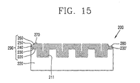
- FIGs. 10 to 15 are views showing a manufacturing method of the light emitting device according to the second embodiment of the present invention.
- a manufacturing method of a light emitting device comprises the steps of: forming a trench portion 211 at a part of an upper surface of a substrate 210 by an etching process using an etching mask 203; forming a buffer layer 210, an n-contact layer 230, an active layer 240, a p-contact layer 250, and a current spreading layer 260 on the upper surface of the substrate 210 where the trench portion 211 is formed; partially removing the active layer 240, the p-contact layer 250, and the current spreading layer 260 so that the n-contact layer 230 can be partially exposed by a mesa patterning processing; forming a p-electrode 270 on an upper surface of the current spreading layer 260 so as to be electrically connected to the active layer 240 and the p-contact layer 250; and forming an n-electrode 280 on an upper surface of the exposed n-contact layer 230 so as to be electrically connected to the n-contact layer
- the etching mask 203 is patterned on an upper surface of the substrate 210 by using an etching process, and then a part of the exposed substrate 210 is etched.
- the substrate is etched by using an anisotropy dry etching method, a wet etching method, or an isotropic dry etching method.
- the buffer layer 220, the n-contact layer 230, the active layer 240, the p-contact layer 250, and the current spreading layer 260 are formed on the entire upper surface of the substrate 210 where the trench portion 211 is formed.
- the semiconductor layer 290 is curvedly formed according to the shape of the trench portion 211. Therefore, a light emitting area of the active layer 240 of the semiconductor layer 290 becomes relatively larger than that of the conventional art thereby to enhance a light emitting efficiency.
- the buffer layer 220 and the n-contact layer 230 are formed by a metal organic chemical vapor deposition (MOCVD) method, a molecular beam epitaxy (MBE) method, or a liquid phase epitaxy (LPE) method.
- MOCVD metal organic chemical vapor deposition
- MBE molecular beam epitaxy
- LPE liquid phase epitaxy
- a photosensitive mask (not shown) is patterned on the p-contact layer 250. Then, an exposure and an etching are performed until a part 130' of the n-contact layer 230 is exposed by a photo etching process and a wet etching process (or a dry etching process), and then the photosensitive mask is removed.
- the p-electrode 270 is formed on an upper surface of the current spreading layer 260 so as to be electrically connected to the active layer 240 and the p-contact layer 250
- the n-electrode 280 is formed on an upper surface of the exposed n-contact layer 230', one part 230' of the n-contact layer 230, thereby completing the light emitting device 200.
- the p-electrode 270 has the same potential as the current spreading layer 260 and the p-contact layer 250
- the n-electrode 280 has the same potential as the n-contact layer 230.
- the trench portion is formed on the substrate of the light emitting device, and then, the buffer layer, the n-contact layer, and active layer are sequentially deposited on the trench portion. According to this, a light emitting area of the active layer is increased thus to obtain light of a high brightness, thereby enhancing a light emitting efficiency and reducing a production cost.
Landscapes
- Led Devices (AREA)
- Electroluminescent Light Sources (AREA)
Abstract
Description
Claims (23)
- A light emitting device comprising:a substrate having a trench portion on an upper surface thereof;a buffer layer formed on the trench portion of the substrate;an n-contact layer formed on an upper surface of the buffer layer;an active layer formed at one side of an upper surface of the n-contact layer;a p-contact layer formed on an upper surface of the active layer;a current spreading layer formed on an upper surface of the p-contact layer;a p-electrode formed on an upper surface of the current spreading layer so as to be electrically connected to the active layer and the p-contact layer; andan n-electrode formed at another side of the upper surface of the n-contact layer so as to be electrically connected to the n-contact layer.
- The device of claim 1, wherein the trench portion is formed at a part of the upper surface of the substrate.
- The device of claim 1, wherein the trench portion is formed at an entire part of the upper surface of the substrate.
- The device of claim 1, wherein the trench portion has a section of a 'V' shape.
- The device of claim 1, wherein the trench portion has a section of a'U'shape.
- The device of claim 1, wherein the current spreading layer is formed of a transparent material.
- The device of claim 1, wherein the current spreading layer is formed of a reflective opaque material.
- A light emitting device comprising:a substrate having a trench portion on an upper surface thereof;a semiconductor layer formed on the substrate;a p-electrode formed on an upper surface of a current spreading layer of the semiconductor layer; andan n-electrode formed on an upper surface of an n-contact layer of the semiconductor layer.
- The device of claim 8, wherein the trench portion has a section of a 'V' shape.
- The device of claim 8, wherein the trench portion has a section of a 'U' shape.
- The device of claim 8, wherein the current spreading layer is formed of a transparent material.
- The device of claim 8, wherein the current spreading layer is formed of either Ni/Au or ITO.
- The device of claim 8, wherein the current spreading layer is formed of a reflective opaque material.
- The device of claim 8, wherein the substrate is formed of sapphire, gallium arsenide, silicon, silicon carbide, or gallium nitride.
- A manufacturing method of a light emitting device comprising the steps of:forming a trench portion on an upper surface of a substrate;forming a buffer layer, an n-contact layer, an active layer, a p-contact layer, and a current spreading layer on the upper surface of the substrate where the trench portion is formed;partially removing the active layer, the p-contact layer, and the current spreading layer by a mesa patterning processing so that the n-contact layer can be partially exposed;forming a p-electrode on an upper surface of the current spreading layer so as to be electrically connected to the active layer and the p-contact layer; andforming an n-electrode on an upper surface of the exposed n-contact layer so as to be electrically connected to the n-contact layer.
- The method of claim 15, wherein the trench portion is formed at an entire part of the upper surface of the substrate.
- The method of claim 15, wherein the trench portion is formed at a part of the upper surface of the substrate.
- The method of claim 15, wherein the trench portion is formed on the upper surface of the substrate by a half cult dicing process.
- The method of claim 15, wherein the trench portion has a section of a 'V' shape.
- The method of claim 15, wherein the trench portion has a section of a 'U' shape.
- The method of claim 15, wherein the buffer layer and the n-contact layer are formed by one of a metal organic chemical vapor deposition (MOCVD) method, a molecular beam epitaxy (MBE) method, and a liquid phase epitaxy (LPE) method.
- The method of claim 15, wherein in the step of forming the trench portion, an etching mask is patterned on the upper surface of the substrate and then an etching process is performed.
- The method of claim 22, wherein the etching process is performed by using one of an anisotropy dry etching method, a wet etching method, and an isotropy dry etching method.
Applications Claiming Priority (2)
| Application Number | Priority Date | Filing Date | Title |
|---|---|---|---|
| KR1020030102255A KR20050071238A (en) | 2003-12-31 | 2003-12-31 | High brightess lighting device and manufacturing method thereof |
| KR2003102255 | 2003-12-31 |
Publications (2)
| Publication Number | Publication Date |
|---|---|
| EP1551064A2 true EP1551064A2 (en) | 2005-07-06 |
| EP1551064A3 EP1551064A3 (en) | 2007-07-25 |
Family
ID=34567876
Family Applications (1)
| Application Number | Title | Priority Date | Filing Date |
|---|---|---|---|
| EP04293146A Withdrawn EP1551064A3 (en) | 2003-12-31 | 2004-12-28 | Light emitting device and manufacturing method thereof. |
Country Status (5)
| Country | Link |
|---|---|
| US (1) | US20050145862A1 (en) |
| EP (1) | EP1551064A3 (en) |
| JP (1) | JP2005197718A (en) |
| KR (1) | KR20050071238A (en) |
| CN (1) | CN1638162A (en) |
Cited By (3)
| Publication number | Priority date | Publication date | Assignee | Title |
|---|---|---|---|---|
| DE102006043400A1 (en) * | 2006-09-15 | 2008-03-27 | Osram Opto Semiconductors Gmbh | Optoelectronic semiconductor chip |
| EP1895601A3 (en) * | 2006-08-28 | 2011-03-16 | Stanley Electric Co., Ltd. | Nitride semiconductor crystal with surface texture |
| CN1897319B (en) * | 2005-07-12 | 2012-03-14 | 三星Led株式会社 | Light emitting diode and method of fabricating the same |
Families Citing this family (27)
| Publication number | Priority date | Publication date | Assignee | Title |
|---|---|---|---|---|
| US7956370B2 (en) * | 2007-06-12 | 2011-06-07 | Siphoton, Inc. | Silicon based solid state lighting |
| US20090032799A1 (en) * | 2007-06-12 | 2009-02-05 | Siphoton, Inc | Light emitting device |
| US8664747B2 (en) * | 2008-04-28 | 2014-03-04 | Toshiba Techno Center Inc. | Trenched substrate for crystal growth and wafer bonding |
| WO2009157921A1 (en) * | 2008-06-24 | 2009-12-30 | Pan Shaoher X | Silicon based solid state lighting |
| KR101533296B1 (en) * | 2008-07-08 | 2015-07-02 | 삼성전자주식회사 | NITRIDE SEMICONDUCTOR LIGHT EMITTING DEVICE HAVING PATTERN FORMED SUBSTRATE |
| US20110114917A1 (en) * | 2008-07-21 | 2011-05-19 | Pan Shaoher X | Light emitting device |
| US8134163B2 (en) | 2008-08-11 | 2012-03-13 | Taiwan Semiconductor Manfacturing Co., Ltd. | Light-emitting diodes on concave texture substrate |
| KR20100024231A (en) | 2008-08-25 | 2010-03-05 | 삼성전자주식회사 | Light emitting element with improved light extraction efficiency, light emitting device comprising the same, and fabricating method of the light emitting element and the light emitting device |
| KR101018590B1 (en) * | 2008-11-20 | 2011-03-03 | 박명일 | Nitride semiconductor light emitting diode |
| US20100308300A1 (en) * | 2009-06-08 | 2010-12-09 | Siphoton, Inc. | Integrated circuit light emission device, module and fabrication process |
| US8674383B2 (en) * | 2010-01-21 | 2014-03-18 | Siphoton Inc. | Solid state lighting device on a conductive substrate |
| US8722441B2 (en) | 2010-01-21 | 2014-05-13 | Siphoton Inc. | Manufacturing process for solid state lighting device on a conductive substrate |
| US8283676B2 (en) * | 2010-01-21 | 2012-10-09 | Siphoton Inc. | Manufacturing process for solid state lighting device on a conductive substrate |
| US8390010B2 (en) * | 2010-03-25 | 2013-03-05 | Micron Technology, Inc. | Solid state lighting devices with cellular arrays and associated methods of manufacturing |
| CN101937953A (en) * | 2010-09-29 | 2011-01-05 | 苏州纳晶光电有限公司 | GaN-based light emitting diode and preparation method thereof |
| US8624292B2 (en) | 2011-02-14 | 2014-01-07 | Siphoton Inc. | Non-polar semiconductor light emission devices |
| US8217418B1 (en) | 2011-02-14 | 2012-07-10 | Siphoton Inc. | Semi-polar semiconductor light emission devices |
| DE102011012925A1 (en) * | 2011-03-03 | 2012-09-06 | Osram Opto Semiconductors Gmbh | Method for producing an optoelectronic semiconductor chip |
| TW201240145A (en) * | 2011-03-21 | 2012-10-01 | Walsin Lihwa Corp | Light emitting diode and method of manufacturing the same |
| CN102185064A (en) * | 2011-04-19 | 2011-09-14 | 武汉华炬光电有限公司 | AlGaN base deep ultraviolet light-emitting diode (LED) device using multiple quantum well electronic barrier layer to improve luminescent efficiency and manufacturing method of AlGaN base deep ultraviolet LED device |
| CN103137798B (en) * | 2011-12-03 | 2015-09-30 | 清华大学 | The preparation method of light-emitting diode |
| CN103367595B (en) * | 2012-03-30 | 2016-02-10 | 展晶科技(深圳)有限公司 | LED crystal particle and manufacture method thereof |
| CN103367583B (en) * | 2012-03-30 | 2016-08-17 | 清华大学 | Light emitting diode |
| CN103367560B (en) * | 2012-03-30 | 2016-08-10 | 清华大学 | The preparation method of light emitting diode |
| TW201401552A (en) * | 2012-06-19 | 2014-01-01 | High Power Optoelectronics Inc | Thermal stress release structure for light emitting diodes |
| US8552457B1 (en) * | 2012-08-07 | 2013-10-08 | High Power Opto. Inc. | Thermal stress releasing structure of a light-emitting diode |
| US10833222B2 (en) | 2016-08-26 | 2020-11-10 | The Penn State Research Foundation | High light extraction efficiency (LEE) light emitting diode (LED) |
Family Cites Families (9)
| Publication number | Priority date | Publication date | Assignee | Title |
|---|---|---|---|---|
| US3359508A (en) * | 1964-02-19 | 1967-12-19 | Gen Electric | High power junction laser structure |
| JPS611069A (en) * | 1984-06-13 | 1986-01-07 | Mitsubishi Electric Corp | Light emitting diode |
| US5481122A (en) * | 1994-07-25 | 1996-01-02 | Industrial Technology Research Institute | Surface light emitting diode with electrically conductive window layer |
| US5814839A (en) * | 1995-02-16 | 1998-09-29 | Sharp Kabushiki Kaisha | Semiconductor light-emitting device having a current adjusting layer and a uneven shape light emitting region, and method for producing same |
| JPH11220170A (en) * | 1998-01-29 | 1999-08-10 | Rohm Co Ltd | Light emitting diode element |
| US6046465A (en) * | 1998-04-17 | 2000-04-04 | Hewlett-Packard Company | Buried reflectors for light emitters in epitaxial material and method for producing same |
| US6514782B1 (en) * | 1999-12-22 | 2003-02-04 | Lumileds Lighting, U.S., Llc | Method of making a III-nitride light-emitting device with increased light generating capability |
| WO2003025263A1 (en) * | 2001-09-13 | 2003-03-27 | Japan Science And Technology Agency | Nitride semiconductor substrate, its manufacturing method, and semiconductor optical device using the same |
| JP4084620B2 (en) * | 2001-09-27 | 2008-04-30 | 信越半導体株式会社 | Light emitting device and method for manufacturing light emitting device |
-
2003
- 2003-12-31 KR KR1020030102255A patent/KR20050071238A/en not_active Withdrawn
-
2004
- 2004-12-28 JP JP2004379004A patent/JP2005197718A/en active Pending
- 2004-12-28 EP EP04293146A patent/EP1551064A3/en not_active Withdrawn
- 2004-12-29 US US11/023,471 patent/US20050145862A1/en not_active Abandoned
- 2004-12-31 CN CN200410103152.0A patent/CN1638162A/en active Pending
Cited By (5)
| Publication number | Priority date | Publication date | Assignee | Title |
|---|---|---|---|---|
| CN1897319B (en) * | 2005-07-12 | 2012-03-14 | 三星Led株式会社 | Light emitting diode and method of fabricating the same |
| EP1895601A3 (en) * | 2006-08-28 | 2011-03-16 | Stanley Electric Co., Ltd. | Nitride semiconductor crystal with surface texture |
| US8158993B2 (en) | 2006-08-28 | 2012-04-17 | Stanley Electric Co., Ltd. | Nitride semiconductor crystal with surface texture |
| US8658440B2 (en) | 2006-08-28 | 2014-02-25 | Stanley Electric Co., Ltd. | Nitride semiconductor crystal with surface texture |
| DE102006043400A1 (en) * | 2006-09-15 | 2008-03-27 | Osram Opto Semiconductors Gmbh | Optoelectronic semiconductor chip |
Also Published As
| Publication number | Publication date |
|---|---|
| US20050145862A1 (en) | 2005-07-07 |
| KR20050071238A (en) | 2005-07-07 |
| EP1551064A3 (en) | 2007-07-25 |
| JP2005197718A (en) | 2005-07-21 |
| CN1638162A (en) | 2005-07-13 |
Similar Documents
| Publication | Publication Date | Title |
|---|---|---|
| EP1551064A2 (en) | Light emitting device and manufacturing method thereof. | |
| US10553744B2 (en) | Diode having high brightness and method thereof | |
| US7682854B2 (en) | Method of making diode having reflective layer | |
| US10032959B2 (en) | Diode having vertical structure | |
| JP4449113B2 (en) | 2D display device | |
| CN114156379A (en) | How to make a light-emitting chip | |
| KR100712890B1 (en) | Light emitting device and manufacturing method | |
| CN118588837B (en) | A light emitting element and a method for preparing the same | |
| KR20050117166A (en) | Method of an optical device using organic substance |
Legal Events
| Date | Code | Title | Description |
|---|---|---|---|
| PUAI | Public reference made under article 153(3) epc to a published international application that has entered the european phase |
Free format text: ORIGINAL CODE: 0009012 |
|
| 17P | Request for examination filed |
Effective date: 20050103 |
|
| AK | Designated contracting states |
Kind code of ref document: A2 Designated state(s): AT BE BG CH CY CZ DE DK EE ES FI FR GB GR HU IE IS IT LI LT LU MC NL PL PT RO SE SI SK TR |
|
| AX | Request for extension of the european patent |
Extension state: AL BA HR LV MK YU |
|
| RIN1 | Information on inventor provided before grant (corrected) |
Inventor name: SONG, KI-CHANG,SANGNOK APT. 106-1003 Inventor name: KIM, GEUN-HO, NOKKYUNG VILLAGE B-102 |
|
| PUAL | Search report despatched |
Free format text: ORIGINAL CODE: 0009013 |
|
| AK | Designated contracting states |
Kind code of ref document: A3 Designated state(s): AT BE BG CH CY CZ DE DK EE ES FI FR GB GR HU IE IS IT LI LT LU MC NL PL PT RO SE SI SK TR |
|
| AX | Request for extension of the european patent |
Extension state: AL BA HR LV MK YU |
|
| AKX | Designation fees paid | ||
| REG | Reference to a national code |
Ref country code: DE Ref legal event code: 8566 |
|
| STAA | Information on the status of an ep patent application or granted ep patent |
Free format text: STATUS: THE APPLICATION IS DEEMED TO BE WITHDRAWN |
|
| 18D | Application deemed to be withdrawn |
Effective date: 20080126 |