EP1551052A2 - Plasma display panel and fabricating method thereof - Google Patents
Plasma display panel and fabricating method thereof Download PDFInfo
- Publication number
- EP1551052A2 EP1551052A2 EP04029507A EP04029507A EP1551052A2 EP 1551052 A2 EP1551052 A2 EP 1551052A2 EP 04029507 A EP04029507 A EP 04029507A EP 04029507 A EP04029507 A EP 04029507A EP 1551052 A2 EP1551052 A2 EP 1551052A2
- Authority
- EP
- European Patent Office
- Prior art keywords
- front substrate
- dielectric layer
- pair
- trench
- sustain electrodes
- Prior art date
- Legal status (The legal status is an assumption and is not a legal conclusion. Google has not performed a legal analysis and makes no representation as to the accuracy of the status listed.)
- Withdrawn
Links
Images



Classifications
-
- H—ELECTRICITY
- H01—ELECTRIC ELEMENTS
- H01J—ELECTRIC DISCHARGE TUBES OR DISCHARGE LAMPS
- H01J11/00—Gas-filled discharge tubes with alternating current induction of the discharge, e.g. alternating current plasma display panels [AC-PDP]; Gas-filled discharge tubes without any main electrode inside the vessel; Gas-filled discharge tubes with at least one main electrode outside the vessel
- H01J11/20—Constructional details
- H01J11/34—Vessels, containers or parts thereof, e.g. substrates
- H01J11/38—Dielectric or insulating layers
-
- H—ELECTRICITY
- H01—ELECTRIC ELEMENTS
- H01J—ELECTRIC DISCHARGE TUBES OR DISCHARGE LAMPS
- H01J11/00—Gas-filled discharge tubes with alternating current induction of the discharge, e.g. alternating current plasma display panels [AC-PDP]; Gas-filled discharge tubes without any main electrode inside the vessel; Gas-filled discharge tubes with at least one main electrode outside the vessel
- H01J11/10—AC-PDPs with at least one main electrode being out of contact with the plasma
- H01J11/12—AC-PDPs with at least one main electrode being out of contact with the plasma with main electrodes provided on both sides of the discharge space
-
- H—ELECTRICITY
- H01—ELECTRIC ELEMENTS
- H01J—ELECTRIC DISCHARGE TUBES OR DISCHARGE LAMPS
- H01J11/00—Gas-filled discharge tubes with alternating current induction of the discharge, e.g. alternating current plasma display panels [AC-PDP]; Gas-filled discharge tubes without any main electrode inside the vessel; Gas-filled discharge tubes with at least one main electrode outside the vessel
- H01J11/20—Constructional details
- H01J11/22—Electrodes, e.g. special shape, material or configuration
- H01J11/24—Sustain electrodes or scan electrodes
-
- H—ELECTRICITY
- H01—ELECTRIC ELEMENTS
- H01J—ELECTRIC DISCHARGE TUBES OR DISCHARGE LAMPS
- H01J11/00—Gas-filled discharge tubes with alternating current induction of the discharge, e.g. alternating current plasma display panels [AC-PDP]; Gas-filled discharge tubes without any main electrode inside the vessel; Gas-filled discharge tubes with at least one main electrode outside the vessel
- H01J11/20—Constructional details
- H01J11/34—Vessels, containers or parts thereof, e.g. substrates
- H01J11/40—Layers for protecting or enhancing the electron emission, e.g. MgO layers
Definitions
- the present invention relates to a plasma display panel, and more particularly, to a plasma display panel and fabricating method thereof, by which brightness thereof is enhanced.
- a plasma display panel in which barrier ribs provided between front and rear glasses formed of soda-lime glass define one unit cell, is a device for implementing pictorial images.
- inert gas such as He-Xe, He-Ne, or the like within each cell is discharged by RF voltage to generate vacuum ultraviolet rays
- phosphor provided between the barrier ribs becomes luminous to implement the pictorial images or video.
- the PDP which facilitates to enable its slim size and wide-screen and has such a feature as low power consumption and the like, is spotlighted.
- PDP is classified into a DC type and an AC type according to an impressed drive voltage waveform and a discharge cell structure.
- the big difference between the AC and DC types lies in that external resistance for current restriction to prevent a discharge current from flowing during voltage impression should be provided to the DC type PDP having electrodes exposed to a discharge space.
- a dielectric layer covers electrodes to naturally form capacitance enabling the current restriction and to protect the electrodes against ionic impact on discharge.
- endurance of the AC type PDP is superior to that of the DC type PDP. For such a reason, it is expected that PDP will adopt the AC drive type.
- the AC drive type PDP is driven in a manner of applying an AC voltage between electrodes having a dielectric inserted therein to trigger discharge each half cycle. Since the AC drive type PDP uses the dielectric, a surface of the dielectric is charged with electricity so that a memory effect can be brought about by a low impressed voltage using the electric charges.
- a configuration of the AC drive type PDP is shown in FIG. 1.
- FIG. 1 is a perspective diagram of a PDP according to a related art.
- a PDP 100 includes a front substrate 10 of an upper panel plate displaying images thereon and a rear substrate 20 of a lower panel plate forming a back face of the PDP 100.
- the front substrate 10 is assembled parallel to the rear substrate 20 to leave a prescribed distance from the rear substrate 20.
- Beneath the front substrate 10 of the upper panel plate a sustain electrode 11 for sustaining light emission of a cell by mutual discharge in one pixel is provided.
- a transparent electrode 11a formed of transparent ITO and a bus electrode 11b formed of a metal based material forms a pair to construct the sustain electrode 11.
- the sustain electrode 11 is covered with a dielectric layer 12 insulating electrode pairs from each other to restrict a discharge current. And, a protective layer 13 is formed by depositing MgO on the dielectric layer 12 to facilitate discharge conditions.
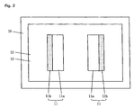
- a layout of the PDP upper plate is shown in FIG. 2.
- a plurality of stripe or well type barrier ribs 21 are arranged parallel to each other to define a plurality of discharge spaces, i.e., a plurality of cells.
- a plurality of address electrodes 22 for generating vacuum ultraviolet rays by performing address discharge in an intersection with the sustain electrode 11 each are arranged parallel to a plurality of the barrier ribs 21, respectively.
- An R/G/B phosphor layer 23 that emits visible rays for image display is coated on the rear substrate 20.
- a black matrix (not shown in the drawing), which is operative in cutting off light to reduce reflection by absorbing external light generated from outside the front substrate 10 and is also operative in enhancing color purity and contrast, is arranged on the barrier ribs 21. And, inert gas such as He + Ne, Ne + Xe, He + Xe + Ne, and the like is injected in the discharge spaces provided between the front substrate 10, the rear substrate 20, and the barrier ribs 21, respectively.
- the image can be displayed by the sustain discharge following the confronting discharge. More specifically, in case that a voltage is applied to the address electrode 22 after voltage impression on the sustain electrode 11, the discharge, i.e., confronting discharge, occurs between the electrodes 22 and 11 to generate ultraviolet rays. And, the generated ultraviolet rays excite the phosphor 23 to emit the visible rays. Thereafter, as a sustain pulse is applied to the sustain electrode pair 11 to trigger the discharge, i.e., sustain discharge, the light emission of the confronting discharge is maintained to implement images.
- FIG. 3 is a cross-sectional diagram of an upper plate according to a related art for explaining a discharge path.
- a discharge path in maintaining the discharge by applying a voltage to the sustain electrode pair 11 on sustain discharge starts from an area (minimum discharge radius R) closest to the sustain electrode 11 and then extends to a distant area (maximum discharge radius R) according to an elapse of sustain discharge time.
- the area of the minimum discharge radius R has the maximum electric field strength, density of electrons and ions formed nearby becomes highest.
- most of the electrons at high temperature i.e., with high energy
- the high density of the electrons and ions increases the density of the ultraviolet rays exciting the phosphor 23, thereby increasing brightness. If the density of the electrons and ions is low, the density of the ultraviolet rays decreases to lower the brightness. Hence, in order to enhance the brightness, a level of the sustain voltage applied to the sustain electrode pair 11 is raised to increase the density of the electrons and ions generated from the sustain discharge.
- an object of the present invention is to solve at least the problems and disadvantages of the background art.
- An object of the present invention is to provide a plasma display panel and fabricating method thereof, by which luminous brightness is enhanced and by which a drive voltage can be lowered.
- a plasma display panel includes a front substrate, a rear substrate confronting the front substrate, a pair of sustain electrodes formed parallel to each other on a confronting surface of the front substrate, a dielectric layer covering the confronting surface of the front substrate and a pair of the sustain electrodes, and a protective layer coated on the dielectric layer, wherein if the dielectric layer and the protective layer configure a functional layer, at least one or more trenches are formed in the functional layer.
- a method of fabricating a plasma display panel which includes a front substrate, a rear substrate confronting the front substrate, a pair of sustain electrodes formed parallel to each other on a confronting surface of the front substrate, a dielectric layer covering the confronting surface of the front substrate and a pair of the sustain electrodes, and a protective layer coated on the dielectric layer wherein if the dielectric layer and the protective layer configure a functional layer, at least one or more trenches are formed in the functional layer, wherein in forming the functional layer, includes the steps of forming the dielectric layer to cover the confronting surface of the front substrate and a pair of the sustain electrodes, forming the trench in the dielectric layer between a pair of the sustain electrodes in a direction vertical to the confronting surface of the front substrate by masking, and forming the protective layer by depositing MgO on the dielectric layer having the trench formed therein and sidewalls of the trench.
- a method of fabricating a plasma display panel which includes a front substrate, a rear substrate confronting the front substrate, a pair of sustain electrodes formed parallel to each other on a confronting surface of the front substrate, a dielectric layer covering the confronting surface of the front substrate and a pair of the sustain electrodes, and a protective layer coated on the dielectric layer wherein if the dielectric layer and the protective layer configure a functional layer, at least one or more trenches are formed in the functional layer, wherein in forming the functional layer, includes the steps of forming the dielectric layer to cover the confronting surface of the front substrate and a pair of the sustain electrodes, forming the trench by etching in a manner of applying a laser to the dielectric layer between a pair of the sustain electrodes in a direction vertical to the confronting surface of the front substrate, and forming the protective layer by depositing MgO on the dielectric layer having the trench formed therein and sidewalls of the trench.
- a discharge space having a high electric field concentrated thereon on discharge expands to increase ultraviolet ray density intensity, whereby more phosphor can be excited to raise brightness. And, if the discharge space expands, it is able to acquire a brightness level equal to that of the related art with a discharge initiation voltage at a level lower than that of the related art.
- FIG. 1 is a perspective diagram of a PDP according to a related art.
- FIG. 2 is a layout of an upper plate of a PDP according to a related art.
- FIG. 3 is a cross-sectional diagram of an upper plate of a PDP according to a related art for explaining a discharge path.
- FIG. 4 is a perspective diagram of a PDP according to the present invention.
- FIG. 5 is a cross-sectional diagram of an upper plate of a PDP according to the present invention.
- FIG. 6 is a cross-sectional diagram of another upper plate of a PDP according to the present invention.
- a plasma display panel includes a front substrate, a rear substrate confronting the front substrate, a pair of sustain electrodes formed parallel to each other on a confronting surface of the front substrate, a dielectric layer covering the confronting surface of the front substrate and a pair of the sustain electrodes, and a protective layer coated on the dielectric layer, wherein if the dielectric layer and the protective layer configure a functional layer, at least one or more trenches are formed in the functional layer.
- the trench is formed between a pair of the sustain electrodes in a direction parallel to each of the sustain electrodes.
- a depth of the trench is 5 ⁇ 30 ⁇ m.
- a width of the trench is 10 ⁇ 50 ⁇ m.
- the trenches are plurally formed in the functional layer.
- the trenches differ from each other in depth and width each.
- the trenches include a central trench formed between a pair of the sustain electrodes and neighbor trenches provided in the vicinity of the central trench and wherein the central trench is greater than each of the neighbor trenches in depth and width.
- a method of fabricating a plasma display panel which includes a front substrate, a rear substrate confronting the front substrate, a pair of sustain electrodes formed parallel to each other on a confronting surface of the front substrate, a dielectric layer covering the confronting surface of the front substrate and a pair of the sustain electrodes, and a protective layer coated on the dielectric layer wherein if the dielectric layer and the protective layer configure a functional layer, at least one or more trenches are formed in the functional layer, wherein in forming the functional layer, includes the steps of forming the dielectric layer to cover the confronting surface of the front substrate and a pair of the sustain electrodes, forming the trench in the dielectric layer between a pair of the sustain electrodes in a direction vertical to the confronting surface of the front substrate by masking, and forming the protective layer by depositing MgO on the dielectric layer having the trench formed therein and sidewalls of the trench.
- a method of fabricating a plasma display panel which includes a front substrate, a rear substrate confronting the front substrate, a pair of sustain electrodes formed parallel to each other on a confronting surface of the front substrate, a dielectric layer covering the confronting surface of the front substrate and a pair of the sustain electrodes, and a protective layer coated on the dielectric layer wherein if the dielectric layer and the protective layer configure a functional layer, at least one or more trenches are formed in the functional layer, wherein in forming the functional layer, includes the steps of forming the dielectric layer to cover the confronting surface of the front substrate and a pair of the sustain electrodes, forming the trench by etching in a manner of applying a laser to the dielectric layer between a pair of the sustain electrodes in a direction vertical to the confronting surface of the front substrate, and forming the protective layer by depositing MgO on the dielectric layer having the trench formed therein and sidewalls of the trench.
- FIG. 4 is a perspective diagram of a PDP according to the present invention.
- a PDP 100 according to the present invention includes a front substrate 10 of an upper panel plate displaying images thereon and a rear substrate 20 of a lower panel plate.
- the front substrate 10 is assembled parallel to the rear substrate 20 to leave a prescribed distance from the rear substrate 20.
- a sustain electrode 11 for sustaining light emission of a cell by mutual discharge in one pixel is provided.
- a transparent electrode 11a formed of transparent ITO and a bus electrode 11b formed of a metal based material forms a pair to construct the sustain electrode 11.
- the sustain electrode 11 is covered with a dielectric layer 12 insulating electrode pairs from each other to restrict a discharge current.
- a protective layer 13 is formed by depositing MgO on the dielectric layer 12 to facilitate discharge conditions.
- the dielectric and protective layers 12 and 13 stacked on the front substrate are called a functional layer A.
- a plurality of stripe or well type barrier ribs 21 are arranged parallel to each other to define a plurality of discharge spaces, i.e., a plurality of cells.
- a plurality of address electrodes 22 for generating vacuum ultraviolet rays by performing address discharge in an intersection with the sustain electrode 11 each are arranged parallel to a plurality of the barrier ribs 21, respectively.
- An R/G/B phosphor layer 23 that emits visible rays for image display is coated on the rear substrate 20.
- a black matrix (not shown in the drawing), which is operative in cutting off light to reduce reflection by absorbing external light generated from outside the front substrate 10 and is also operative in enhancing color purity and contrast, is arranged on the barrier ribs 21.
- the dielectric layer 12 is formed on the transparent electrode 11a and the bus electrode 11b by screen printing. In doing so, a trench 14 is formed in the dielectric layer 12 in a direction vertical to the front substrate and MgO is then deposited on the dielectric layer 12 to form the protective layer 13.
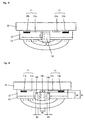
- FIG. 5 is a cross-sectional diagram of an upper plate of a PDP according to the present invention.
- the trench 14 is formed in the functional layer A, which consists of the dielectric layer 12 and the protective layer 13, in the vertical direction to the front substrate 10.
- the trench 14 is formed between the sustain electrode pairs 11 adjacent to each other in a direction parallel to the sustain electrode 11.
- a method of fabricating an upper plate of the above-configured PDP according to the present invention is explained as follows. First of all, a dielectric is coated on the front substrate having the sustain electrode pairs 11 formed thereon to form the dielectric layer 12. Subsequently, the trench 14 is formed in the dielectric layer 12 over a middle portion between the sustain electrode pairs 11 adjacent to each other in a direction vertical to the front substrate by masking. Thereafter, Mgo is deposited on the dielectric layer 12 including sidewalls of the trench 14 to form the protective layer.
- the PDP including the functional layer having the trench formed therein triggers the sustain discharge by the impression of the sustain pulse on the sustain electrode pairs to maintain the corresponding light emission.
- the sustain discharge starts from an area closest to the sustain electrode 11 and then extends to a distant area according to an elapse of sustain discharge time.
- the trench provided to the functional layer works as a new discharge space to play a role as a discharge space having a high electric field concentrated thereon. Namely, most of electrons with high energy are concentrated on the trench to intensively bring about the ionization and excitation so that powerful ultraviolet rays can excite the phosphor, whereby brightness is enhanced.
- the trench is formed deeper to expand the discharge space having the electric field concentrated thereon in the trench provided to the functional layer.
- a depth d of the trench is defined to lie within a range of 5 ⁇ 30 ⁇ m.
- a width w of the trench is defined to lie within a range of 10 ⁇ 50 ⁇ m.
- FIG. 6 is a cross-sectional diagram of another upper plate of a PDP according to the present invention.
- a plurality of trenches 14 are formed in the functional layer A consisting of the dielectric layer 12 and the protective layer 13 in the direction vertical to the front substrate.
- a plurality of the trenches 14 include a central trench 14a and neighbor trenches 14b.
- a depth d1 and width w1 of the central trench 14a are formed greater than a depth d2 and width w2 of each of the neighbor trenches 14b, respectively.
- a discharge space having a high electric field concentrated thereon on discharge expands to increase ultraviolet ray density intensity, whereby more phosphor can be excited to raise brightness.
- the discharge space expands, it is able to acquire a brightness level equal to that of the related art with a discharge initiation voltage at a level lower than that of the related art.
Landscapes
- Engineering & Computer Science (AREA)
- Physics & Mathematics (AREA)
- Plasma & Fusion (AREA)
- Chemical & Material Sciences (AREA)
- Materials Engineering (AREA)
- Gas-Filled Discharge Tubes (AREA)
Abstract
a protective layer (13) coated on the dielectric layer (12), wherein if the dielectric layer (12) and the protective layer (13) configure a functional layer, at least one or more trenches (14) are formed in the functional layer. By the present invention, a discharge space having a high electric field concentrated thereon on discharge expands to increase ultraviolet ray density intensity, whereby more phosphor can be excited to raise brightness. And, if the discharge space expands, it is able to acquire a brightness level equal to that of the related art with a discharge initiation voltage at a level lower than that of the related art.
Description
Claims (9)
- A plasma display panel comprising:wherein if the dielectric layer and the protective layer configure a functional layer, at least one or more trenches are formed in the functional layer.a front substrate;a rear substrate confronting the front substrate;a pair of sustain electrodes formed parallel to each other on a confronting surface of the front substrate;a dielectric layer covering the confronting surface of the front substrate and a pair of the sustain electrodes; anda protective layer coated on the dielectric layer,
- The plasma display panel of claim 1, wherein the trench is formed between a pair of the sustain electrodes in a direction parallel to each of the sustain electrodes.
- The plasma display panel of claim 1 or claim 2, wherein a depth of the trench is 5 ~ 30µm.
- The plasma display panel of claim 1 or claim 2, wherein a width of the trench is 10 ~ 50µm.
- The plasma display panel of claim 1 or claim 2, wherein the trenches are at least one or more, formed in the functional layer
- The plasma display panel of claim 5, wherein the trenches differ in depth and width each.
- The plasma display panel of claim 5, wherein the trenches comprise a central trench formed between a pair of the sustain electrodes and neighbor trenches provided in the vicinity of the central trench and wherein the central trench is greater than each of the neighbor trenches in depth and width.
- A method of fabricating a plasma display panel which includes a front substrate, a rear substrate confronting the front substrate, a pair of sustain electrodes formed parallel to each other on a confronting surface of the front substrate, a dielectric layer covering the confronting surface of the front substrate and a pair of the sustain electrodes, and a protective layer coated on the dielectric layer wherein if the dielectric layer and the protective layer configure a functional layer, at least one or more trenches are formed in the functional layer, wherein in forming the functional layer,
the method includes the steps of forming the dielectric layer to cover the confronting surface of the front substrate and a pair of the sustain electrodes, forming the trench in the dielectric layer between a pair of the sustain electrodes in a direction vertical to the confronting surface of the front substrate by masking, and forming the protective layer by depositing MgO on the dielectric layer having the trench formed therein and sidewalls of the trench. - A method of fabricating a plasma display panel which includes a front substrate, a rear substrate confronting the front substrate, a pair of sustain electrodes formed parallel to each other on a confronting surface of the front substrate, a dielectric layer covering the confronting surface of the front substrate and a pair of the sustain electrodes, and a protective layer coated on the dielectric layer wherein if the dielectric layer and the protective layer configure a functional layer, at least one or more trenches are formed in the functional layer, wherein in forming the functional layer,
the method includes the steps of forming the dielectric layer to cover the confronting surface of the front substrate and a pair of the sustain electrodes, forming the trench by etching in a manner of applying a laser to the dielectric layer between a pair of the sustain electrodes in a direction vertical to the confronting surface of the front substrate, and forming the protective layer by depositing MgO on the dielectric layer having the trench formed therein and sidewalls of the trench.
Applications Claiming Priority (2)
| Application Number | Priority Date | Filing Date | Title |
|---|---|---|---|
| KR2003102319 | 2003-12-31 | ||
| KR1020030102319A KR20050071268A (en) | 2003-12-31 | 2003-12-31 | Plasma display panel and methode of making thereof |
Publications (2)
| Publication Number | Publication Date |
|---|---|
| EP1551052A2 true EP1551052A2 (en) | 2005-07-06 |
| EP1551052A3 EP1551052A3 (en) | 2006-07-05 |
Family
ID=34567877
Family Applications (1)
| Application Number | Title | Priority Date | Filing Date |
|---|---|---|---|
| EP04029507A Withdrawn EP1551052A3 (en) | 2003-12-31 | 2004-12-14 | Plasma display panel and fabricating method thereof |
Country Status (4)
| Country | Link |
|---|---|
| US (1) | US7276850B2 (en) |
| EP (1) | EP1551052A3 (en) |
| JP (1) | JP2005197232A (en) |
| KR (1) | KR20050071268A (en) |
Families Citing this family (6)
| Publication number | Priority date | Publication date | Assignee | Title |
|---|---|---|---|---|
| KR100573130B1 (en) * | 2003-11-29 | 2006-04-24 | 삼성에스디아이 주식회사 | Plasma display panel and manufacturing method thereof |
| KR20050105703A (en) * | 2004-05-03 | 2005-11-08 | 삼성에스디아이 주식회사 | Plasma display panel |
| KR100670324B1 (en) * | 2005-03-23 | 2007-01-16 | 삼성에스디아이 주식회사 | Plasma display panel |
| KR100658721B1 (en) * | 2005-05-31 | 2006-12-15 | 삼성에스디아이 주식회사 | Plasma display panel |
| KR100726643B1 (en) * | 2005-07-01 | 2007-06-08 | 엘지전자 주식회사 | Plasma Display Panel And Method Of Manufacturing The Same |
| KR20070097949A (en) * | 2006-03-30 | 2007-10-05 | 엘지전자 주식회사 | Plasma Display Panel And Method Of Manufacturing The Same |
Family Cites Families (8)
| Publication number | Priority date | Publication date | Assignee | Title |
|---|---|---|---|---|
| KR20000007610A (en) * | 1998-07-04 | 2000-02-07 | 구자홍 | Plasma display device having separative dielectric film and protection film and method of the same |
| JP2001189132A (en) * | 2000-01-05 | 2001-07-10 | Sony Corp | AC driven plasma display device and method of manufacturing the same |
| CN101090054B (en) * | 2000-01-26 | 2010-05-26 | 松下电器产业株式会社 | Surface discharge type display device with excellent power consumption suppression effect |
| US7348729B2 (en) * | 2000-08-29 | 2008-03-25 | Matsushita Electric Industrial Co., Ltd. | Plasma display panel and production method thereof and plasma display panel display unit |
| JP3442069B2 (en) * | 2001-05-28 | 2003-09-02 | 松下電器産業株式会社 | Plasma display panel, method of manufacturing the same, and transfer film |
| JP2003151445A (en) * | 2001-11-09 | 2003-05-23 | Pioneer Electronic Corp | Plasma display panel and its driving method |
| JP4145054B2 (en) * | 2002-02-06 | 2008-09-03 | パイオニア株式会社 | Plasma display panel |
| KR100557907B1 (en) * | 2002-03-06 | 2006-03-10 | 마쯔시다덴기산교 가부시키가이샤 | Plasma display device |
-
2003
- 2003-12-31 KR KR1020030102319A patent/KR20050071268A/en not_active Ceased
-
2004
- 2004-12-01 US US11/000,010 patent/US7276850B2/en not_active Expired - Fee Related
- 2004-12-08 JP JP2004354829A patent/JP2005197232A/en not_active Abandoned
- 2004-12-14 EP EP04029507A patent/EP1551052A3/en not_active Withdrawn
Also Published As
| Publication number | Publication date |
|---|---|
| EP1551052A3 (en) | 2006-07-05 |
| US20050140299A1 (en) | 2005-06-30 |
| US7276850B2 (en) | 2007-10-02 |
| JP2005197232A (en) | 2005-07-21 |
| KR20050071268A (en) | 2005-07-07 |
Similar Documents
| Publication | Publication Date | Title |
|---|---|---|
| JP4339298B2 (en) | Plasma display panel | |
| US7276850B2 (en) | Plasma display panel having trenches in functional layer | |
| JP2006140144A (en) | Plasma display panel | |
| KR100683668B1 (en) | Plasma display panel | |
| EP1646065A2 (en) | Plasma display panel and plasma display apparatus comprising electrodes | |
| KR100603325B1 (en) | Plasma display panel | |
| US7420329B2 (en) | Plasma display panel (PDP) | |
| US7557506B2 (en) | Plasma display panel | |
| JP2005327712A (en) | Plasma display panel | |
| KR100787443B1 (en) | Plasma display panel | |
| KR100741767B1 (en) | Plasma display panel | |
| US7605539B2 (en) | Plasma display panel with reduced electrode defect rate | |
| KR100275314B1 (en) | Plasma display panel | |
| KR100613013B1 (en) | Plasma display panel | |
| KR100669723B1 (en) | Plasma display panel | |
| KR100674832B1 (en) | Plasma display panel | |
| KR100718996B1 (en) | Plasma Display Panel Including Electrodes | |
| KR100708733B1 (en) | Plasma display panel | |
| KR20010076096A (en) | Plasma display panel and method of driving the same | |
| KR100670303B1 (en) | Plasma display panel | |
| KR100813837B1 (en) | Plasma display panel | |
| KR100705803B1 (en) | Plasma display panel | |
| KR100490531B1 (en) | plasma display panel | |
| KR100581955B1 (en) | Plasma display panel | |
| KR20060062484A (en) | Plasma display panel |
Legal Events
| Date | Code | Title | Description |
|---|---|---|---|
| PUAI | Public reference made under article 153(3) epc to a published international application that has entered the european phase |
Free format text: ORIGINAL CODE: 0009012 |
|
| AK | Designated contracting states |
Kind code of ref document: A2 Designated state(s): AT BE BG CH CY CZ DE DK EE ES FI FR GB GR HU IE IS IT LI LT LU MC NL PL PT RO SE SI SK TR |
|
| AX | Request for extension of the european patent |
Extension state: AL BA HR LV MK YU |
|
| PUAL | Search report despatched |
Free format text: ORIGINAL CODE: 0009013 |
|
| AK | Designated contracting states |
Kind code of ref document: A3 Designated state(s): AT BE BG CH CY CZ DE DK EE ES FI FR GB GR HU IE IS IT LI LT LU MC NL PL PT RO SE SI SK TR |
|
| AX | Request for extension of the european patent |
Extension state: AL BA HR LV MK YU |
|
| RIC1 | Information provided on ipc code assigned before grant |
Ipc: H01J 9/24 20060101ALI20060529BHEP Ipc: H01J 17/49 20060101AFI20050422BHEP |
|
| 17P | Request for examination filed |
Effective date: 20061216 |
|
| AKX | Designation fees paid |
Designated state(s): DE FR GB NL |
|
| 17Q | First examination report despatched |
Effective date: 20070912 |
|
| STAA | Information on the status of an ep patent application or granted ep patent |
Free format text: STATUS: THE APPLICATION HAS BEEN WITHDRAWN |
|
| 18W | Application withdrawn |
Effective date: 20090423 |