EP1550850A1 - Read/Write device for a mass storage device, and Read/Write method thereof - Google Patents
Read/Write device for a mass storage device, and Read/Write method thereof Download PDFInfo
- Publication number
- EP1550850A1 EP1550850A1 EP03425826A EP03425826A EP1550850A1 EP 1550850 A1 EP1550850 A1 EP 1550850A1 EP 03425826 A EP03425826 A EP 03425826A EP 03425826 A EP03425826 A EP 03425826A EP 1550850 A1 EP1550850 A1 EP 1550850A1
- Authority
- EP
- European Patent Office
- Prior art keywords
- data
- read
- storage device
- bipolar junction
- storage medium
- Prior art date
- Legal status (The legal status is an assumption and is not a legal conclusion. Google has not performed a legal analysis and makes no representation as to the accuracy of the status listed.)
- Withdrawn
Links
- 238000000034 method Methods 0.000 title claims description 17
- 238000003860 storage Methods 0.000 title description 12
- 238000013500 data storage Methods 0.000 claims abstract description 30
- 239000000758 substrate Substances 0.000 claims abstract description 13
- 239000000523 sample Substances 0.000 claims abstract description 9
- 239000004065 semiconductor Substances 0.000 claims abstract description 6
- 239000000463 material Substances 0.000 claims abstract description 5
- 229910052710 silicon Inorganic materials 0.000 claims description 14
- 239000010703 silicon Substances 0.000 claims description 14
- 230000002596 correlated effect Effects 0.000 claims 1
- 229920006254 polymer film Polymers 0.000 description 19
- 238000007373 indentation Methods 0.000 description 15
- XUIMIQQOPSSXEZ-UHFFFAOYSA-N Silicon Chemical compound [Si] XUIMIQQOPSSXEZ-UHFFFAOYSA-N 0.000 description 13
- 230000007423 decrease Effects 0.000 description 6
- 239000002019 doping agent Substances 0.000 description 5
- 241000258963 Diplopoda Species 0.000 description 4
- 125000004429 atom Chemical group 0.000 description 4
- 238000010438 heat treatment Methods 0.000 description 4
- 229910052751 metal Inorganic materials 0.000 description 4
- 239000002184 metal Substances 0.000 description 4
- 238000001514 detection method Methods 0.000 description 3
- 230000006870 function Effects 0.000 description 3
- 238000005459 micromachining Methods 0.000 description 3
- 229910052581 Si3N4 Inorganic materials 0.000 description 2
- 238000010586 diagram Methods 0.000 description 2
- 238000005516 engineering process Methods 0.000 description 2
- 230000017525 heat dissipation Effects 0.000 description 2
- 238000004519 manufacturing process Methods 0.000 description 2
- 229920003229 poly(methyl methacrylate) Polymers 0.000 description 2
- 239000004926 polymethyl methacrylate Substances 0.000 description 2
- HQVNEWCFYHHQES-UHFFFAOYSA-N silicon nitride Chemical compound N12[Si]34N5[Si]62N3[Si]51N64 HQVNEWCFYHHQES-UHFFFAOYSA-N 0.000 description 2
- ZOXJGFHDIHLPTG-UHFFFAOYSA-N Boron Chemical group [B] ZOXJGFHDIHLPTG-UHFFFAOYSA-N 0.000 description 1
- ZOKXTWBITQBERF-UHFFFAOYSA-N Molybdenum Chemical compound [Mo] ZOKXTWBITQBERF-UHFFFAOYSA-N 0.000 description 1
- VYPSYNLAJGMNEJ-UHFFFAOYSA-N Silicium dioxide Chemical compound O=[Si]=O VYPSYNLAJGMNEJ-UHFFFAOYSA-N 0.000 description 1
- 230000015572 biosynthetic process Effects 0.000 description 1
- 230000015556 catabolic process Effects 0.000 description 1
- 239000002800 charge carrier Substances 0.000 description 1
- 238000003486 chemical etching Methods 0.000 description 1
- 238000005229 chemical vapour deposition Methods 0.000 description 1
- 238000001816 cooling Methods 0.000 description 1
- 230000010259 detection of temperature stimulus Effects 0.000 description 1
- 230000000694 effects Effects 0.000 description 1
- 230000012447 hatching Effects 0.000 description 1
- 230000005389 magnetism Effects 0.000 description 1
- 238000012986 modification Methods 0.000 description 1
- 230000004048 modification Effects 0.000 description 1
- 229910052750 molybdenum Inorganic materials 0.000 description 1
- 239000011733 molybdenum Substances 0.000 description 1
- 125000004437 phosphorous atom Chemical group 0.000 description 1
- 238000001259 photo etching Methods 0.000 description 1
- 230000000704 physical effect Effects 0.000 description 1
- 238000001020 plasma etching Methods 0.000 description 1
- 229920000642 polymer Polymers 0.000 description 1
- 238000005215 recombination Methods 0.000 description 1
- 230000006798 recombination Effects 0.000 description 1
- 230000001105 regulatory effect Effects 0.000 description 1
- 229910052814 silicon oxide Inorganic materials 0.000 description 1
- 239000011232 storage material Substances 0.000 description 1
- 239000000126 substance Substances 0.000 description 1
- 238000004804 winding Methods 0.000 description 1
Images


Classifications
-
- G—PHYSICS
- G01—MEASURING; TESTING
- G01K—MEASURING TEMPERATURE; MEASURING QUANTITY OF HEAT; THERMALLY-SENSITIVE ELEMENTS NOT OTHERWISE PROVIDED FOR
- G01K7/00—Measuring temperature based on the use of electric or magnetic elements directly sensitive to heat ; Power supply therefor, e.g. using thermoelectric elements
- G01K7/01—Measuring temperature based on the use of electric or magnetic elements directly sensitive to heat ; Power supply therefor, e.g. using thermoelectric elements using semiconducting elements having PN junctions
-
- B—PERFORMING OPERATIONS; TRANSPORTING
- B82—NANOTECHNOLOGY
- B82Y—SPECIFIC USES OR APPLICATIONS OF NANOSTRUCTURES; MEASUREMENT OR ANALYSIS OF NANOSTRUCTURES; MANUFACTURE OR TREATMENT OF NANOSTRUCTURES
- B82Y10/00—Nanotechnology for information processing, storage or transmission, e.g. quantum computing or single electron logic
-
- G—PHYSICS
- G11—INFORMATION STORAGE
- G11B—INFORMATION STORAGE BASED ON RELATIVE MOVEMENT BETWEEN RECORD CARRIER AND TRANSDUCER
- G11B9/00—Recording or reproducing using a method not covered by one of the main groups G11B3/00 - G11B7/00; Record carriers therefor
- G11B9/12—Recording or reproducing using a method not covered by one of the main groups G11B3/00 - G11B7/00; Record carriers therefor using near-field interactions; Record carriers therefor
- G11B9/14—Recording or reproducing using a method not covered by one of the main groups G11B3/00 - G11B7/00; Record carriers therefor using near-field interactions; Record carriers therefor using microscopic probe means, i.e. recording or reproducing by means directly associated with the tip of a microscopic electrical probe as used in Scanning Tunneling Microscopy [STM] or Atomic Force Microscopy [AFM] for inducing physical or electrical perturbations in a recording medium; Record carriers or media specially adapted for such transducing of information
-
- G—PHYSICS
- G11—INFORMATION STORAGE
- G11B—INFORMATION STORAGE BASED ON RELATIVE MOVEMENT BETWEEN RECORD CARRIER AND TRANSDUCER
- G11B9/00—Recording or reproducing using a method not covered by one of the main groups G11B3/00 - G11B7/00; Record carriers therefor
- G11B9/12—Recording or reproducing using a method not covered by one of the main groups G11B3/00 - G11B7/00; Record carriers therefor using near-field interactions; Record carriers therefor
- G11B9/14—Recording or reproducing using a method not covered by one of the main groups G11B3/00 - G11B7/00; Record carriers therefor using near-field interactions; Record carriers therefor using microscopic probe means, i.e. recording or reproducing by means directly associated with the tip of a microscopic electrical probe as used in Scanning Tunneling Microscopy [STM] or Atomic Force Microscopy [AFM] for inducing physical or electrical perturbations in a recording medium; Record carriers or media specially adapted for such transducing of information
- G11B9/1409—Heads
-
- C—CHEMISTRY; METALLURGY
- C08—ORGANIC MACROMOLECULAR COMPOUNDS; THEIR PREPARATION OR CHEMICAL WORKING-UP; COMPOSITIONS BASED THEREON
- C08L—COMPOSITIONS OF MACROMOLECULAR COMPOUNDS
- C08L2201/00—Properties
- C08L2201/12—Shape memory
-
- G—PHYSICS
- G01—MEASURING; TESTING
- G01Q—SCANNING-PROBE TECHNIQUES OR APPARATUS; APPLICATIONS OF SCANNING-PROBE TECHNIQUES, e.g. SCANNING PROBE MICROSCOPY [SPM]
- G01Q80/00—Applications, other than SPM, of scanning-probe techniques
-
- G—PHYSICS
- G11—INFORMATION STORAGE
- G11B—INFORMATION STORAGE BASED ON RELATIVE MOVEMENT BETWEEN RECORD CARRIER AND TRANSDUCER
- G11B11/00—Recording on or reproducing from the same record carrier wherein for these two operations the methods are covered by different main groups of groups G11B3/00 - G11B7/00 or by different subgroups of group G11B9/00; Record carriers therefor
- G11B11/03—Recording on or reproducing from the same record carrier wherein for these two operations the methods are covered by different main groups of groups G11B3/00 - G11B7/00 or by different subgroups of group G11B9/00; Record carriers therefor using recording by deforming with non-mechanical means, e.g. laser, beam of particles
-
- G—PHYSICS
- G11—INFORMATION STORAGE
- G11B—INFORMATION STORAGE BASED ON RELATIVE MOVEMENT BETWEEN RECORD CARRIER AND TRANSDUCER
- G11B11/00—Recording on or reproducing from the same record carrier wherein for these two operations the methods are covered by different main groups of groups G11B3/00 - G11B7/00 or by different subgroups of group G11B9/00; Record carriers therefor
- G11B11/16—Recording on or reproducing from the same record carrier wherein for these two operations the methods are covered by different main groups of groups G11B3/00 - G11B7/00 or by different subgroups of group G11B9/00; Record carriers therefor using recording by mechanical cutting, deforming or pressing
-
- G—PHYSICS
- G11—INFORMATION STORAGE
- G11B—INFORMATION STORAGE BASED ON RELATIVE MOVEMENT BETWEEN RECORD CARRIER AND TRANSDUCER
- G11B13/00—Recording simultaneously or selectively by methods covered by different main groups among G11B3/00, G11B5/00, G11B7/00 and G11B9/00; Record carriers therefor not otherwise provided for; Reproducing therefrom not otherwise provided for
-
- G—PHYSICS
- G11—INFORMATION STORAGE
- G11B—INFORMATION STORAGE BASED ON RELATIVE MOVEMENT BETWEEN RECORD CARRIER AND TRANSDUCER
- G11B5/00—Recording by magnetisation or demagnetisation of a record carrier; Reproducing by magnetic means; Record carriers therefor
- G11B2005/0002—Special dispositions or recording techniques
- G11B2005/0005—Arrangements, methods or circuits
- G11B2005/0021—Thermally assisted recording using an auxiliary energy source for heating the recording layer locally to assist the magnetization reversal
Definitions
- the present invention relates to a read/write device for a mass storage device.
- the data-storage system proposed by IBM and referred to as "Millipede” exploits a type of technology based upon silicon nanometric read/write heads, similar to the ones used in atomic-force microscopes (AFMs) or in scanning tunnelling microscopes (STMs) to obtain images at an atomic scale.
- AFMs atomic-force microscopes
- STMs scanning tunnelling microscopes
- a mass storage device 1 As illustrated in the figure, a mass storage device 1 according to the "Millipede" system is made up by a two-dimensional array 2 of cantilever elements 3, of silicon, which are obtained exploiting micromachining techniques and are fixed to a common substrate 4, also of silicon.
- Each of the cantilever elements 3 functions as a support for a respective read/write (R/W) head 6 formed at the end of the respective cantilever element 3.
- a polymer film 5 for example of polymethylmethacrylate (PMMA) and operating as a data-storage material, extends underneath the two-dimensional array 2 and has the thickness of some tens of nanometres.
- PMMA polymethylmethacrylate
- Each individual R/W head 6 can be driven for reading or writing via an addressing technique similar to the one commonly used in DRAMs, hence through two multiplexers 10, 11 which select respectively the rows and columns of the two-dimensional array 2.
- the polymer film 5 is located on a mobile platform 12, which is moved in the directions x, y and z by an actuating system (not shown) comprising miniaturized windings and permanent magnets.
- Each R/W head 6 acts within an own restricted data-storage area, typically of the order of 100 ⁇ m 2 , so that, for example, in a 32x32 array, 1024 R/W heads 6 are present.
- Each cantilever element 3 stores data through the respective R/W head 6, by forming, in the polymer film 5, indentations 14 (shown only schematically in Figure 1) having a width and a space between them of some tens of nanometres.
- the presence or absence of an indentation 14 encodes a datum to be stored in a binary way (for example, the presence of an indentation can represent a "1", whilst the absence of an indentation can represent a "0").
- the indentations 14 are created by applying a local force on the polymer film 5 via the R/W heads 6 and, at the same time, by heating locally the polymer film 5 at high temperature (approximately 400°C). Heating is performed by a heater element of resistive type here made of a silicon monocrystal with low doping level, arranged at the R/W head 6 and passed by an electric current.
- a heater element of resistive type here made of a silicon monocrystal with low doping level
- Reading is carried out using the heater element as a temperature sensor, exploiting the variation in its resistance as a function of the temperature.
- the resistance of the heater element increases with the temperature in a non-linear way starting from room temperature up to a peak value comprised between 500°C and 700°C, which depends upon the concentration of dopant in the heater element.
- the heater element is heated at a constant temperature of approximately 350°C, a temperature which does not cause softening of the polymer film 5 but is sufficient to create a temperature gradient with respect to the polymer film 5, as is necessary to read the data.
- heat is transferred between the R/W head 6 and the polymer film 5, through the air, and the heat transfer becomes more efficient when the distance between the two elements decreases, i.e., when the R/W head 6 moves inside an indentation 14. Consequently, when the R/W head 6 is in the indentation 14, the temperature of the heater element decreases, and consequently its resistance is reduced.
- the variation in resistance of the heater element can thus be used for reading the stored data.
- Stored data erasing can occur according to two different modes, as described hereinafter.
- An entire data block can be erased by heating the polymer film 5 at a high temperature for a few seconds. After cooling, the surface of the polymer film 5 becomes uniform again.
- an individual data bit is erased by bringing the R/W head 6 in write mode to a point adjacent to the indentation 14 to be erased.
- polymer molecules are concentrated on account of the previous formation of the indentation 14, which, on account of the force exerted by the R/W head 6, are now forced to redistribute uniformly, thus causing an effect of evening-out which removes the stored information.
- the described device enables data-storage capacities of the order of the terabits to be obtained in an extremely small space (a few tens of square millimetres).
- the aim of the present invention is to provide a read/write device of the described type, which will be free from the drawbacks described in detail above.
- a read/write device for a mass storage device is provided, as defined in claim 1.
- a read/write device 20 belonging to a mass storage device of the above type, i.e., comprising a polymer film that can be written by making indentations.
- the read/write device 20 is considered as belonging to a mass storage device 1 of the type described with reference to Figure 1. Consequently, the elements that are in common with the ones of Figure 1 are designated by the same reference numbers.
- the invention is not limited to this specific application, but can advantageously be used also in other data-storage systems, provided, for example, with different supporting, moving and/or addressing systems.
- the read/write device 20 comprises a substrate 4 of semiconductor material (for example, silicon) having at least one cavity 22 and coated with an insulating layer 23, open at the cavity 22.
- the substrate 4 comprises a plurality of cavities 22.
- a read/write element 3 extends above each cavity 22 and is formed by a pair of arms 25 and 26, of silicon, joined together to form generally a "V".
- Each arm 25, 26 has an anchorage end 25a, 26a, fixed to the substrate 4 (through the insulating layer 23), and a free end 25b, 26b, and extends in cantilever fashion for the most part of its length above the cavity 22.
- a tip 6, of silicon, is carried by the free ends 25b, 26b (that are connected together) and extends away from the cavity 22, i.e., towards the polymer film 5, here shown only partially with hatching.
- Stress regions 28, of silicon nitride extend above each of the arms 25 and 26, next to their anchorage ends 25a, 26a. In a per se known manner, deformation of the stress regions 28 can be controlled in order to bend the arms 25 and 26 away from the surface of the substrate 4 by a few micrometres in order to bring the tip 6 near to the polymer film 5.
- Contact metal regions 29 and 30 extend above and are in electrical contact with the anchorage ends 25a, 26a of the arms 25, 26.
- Metal paths extend from the contact metal regions 29 and 30 for addressing the individual pair of arms 25, 26 belonging to the read/write device 20 and the passage of an electric current I ( Figure 3) through the arms 25 and 26.
- the arms 25 and 26 are doped in opposite ways; specifically, a first arm (for example, the arm 25) is doped with a high concentration of P-type dopant atoms (P + doping), and a second arm (for example the arm 26) is doped with a high concentration of N-type dopant atoms (N + doping) so as to provide a bipolar junction 31 at the contact area between the free ends 25b, 26b of the arms 25 and 26.
- P + doping P-type dopant atoms
- N + doping N-type dopant atoms
- Figures 3 and 4 show, in particular, a perspective cross section of the read/write device 20 next to the free ends 25b, 26b, highlighting the tip 6 and a diode formed by the bipolar junction 31.
- Figures 3 and 4 further illustrate an indentation 32 formed in the polymer film 5 for storing a datum, resulting from a write operation.
- the read/write device 20 can be manufactured using known micromachining techniques, for example using a CMOS-compatible process, starting from an SOI wafer, comprising a substrate (the aforementioned substrate 4), a silicon-oxide layer (insulating layer 23), and a silicon top layer, for example with the thickness of 100 ⁇ m.
- the silicon top layer is etched via an appropriate photo-etching technique in order to form the arms 25 and 26. Then the arms 25 and 26 undergo N-type and P-type doping, as specified above.
- the dopant atoms for example, boron atoms for P-type doping and phosphorus atoms for N-type doping
- the dopant atoms are diffused throughout the thickness of the silicon top layer that forms the arms 25 and 26.
- the cavity 22 is formed in the insulating layer 23 and partly in the substrate 4 underneath the arms 25 and 26, for example, via chemical or plasma etching, and a silicon-nitride layer is deposited (for example, via a chemical-vapour-deposition -CVD- technique) and defined to form the stress regions 28 at the base of the arms 25 and 26.
- the contact metal regions 29 and 30 are formed, for instance of molybdenum.
- an indentation 32 is formed on the surface of the polymer film 5 via application of heat and of a local force on the polymer film 5 through the tip 6.
- heating is obtained by applying a voltage of 5-6 V, which causes the passage of a relatively high electric current across the arms 25 and 26.
- Reading of the datum is carried out by supplying a constant current to the bipolar junction 31 and measuring the temperature thereof.
- the known property of forward-biased bipolar junctions is exploited, i.e. the voltage of the junction decreases markedly as the temperature increases, typically in the proportion of approximately -2 mV/°C, as is shown in Figure 5 and described by the following equation: where I D is the biasing current, I 0 is the reverse saturation current of the junction, V J is the junction voltage, T is the junction temperature, V T is the volt equivalent of temperature at 25°C, and ⁇ is a parameter that takes into account the phenomena of generation and recombination of the charge carriers within the junction.
- Figure 5 shows three curves obtained at three different junction temperatures, T 1 , T 2 and T 3 , with T 3 ⁇ T 2 ⁇ T 1 .
- the forward-biasing current I REF is kept constant, the junction voltage V J increases as the junction temperature decreases.
- the bipolar junction 31 is directly biased with a constant current IRE F and the junction voltage V J is acquired, it is hence possible to derive the value of the bit stored.
- the read/write device 20 comprises one or more dummy elements, which have the same structure as the read/write elements 3 and can be used as references during reading so as to prevent undesired changes of temperature and/or of biasing current from causing data reading errors (offset compensation).
- the dummy elements are not bent and hence do not present the stress region 28 at the base of the arms 25 and 26.
- the dummy elements can be used, for example, in the read circuit 40 shown in Figure 6 and integrated in the mass storage device 1 of Figure 1.
- the read circuit 40 comprises two current sources 41, which are equal to one another, connected respectively to a read/write element 3 of the type shown in Figures 2-4 and to a dummy element, here designated by 42.
- the current sources 41 supply constant currents I REF and can be obtained via a single current-mirror circuit (not shown) with two outputs.
- the read circuit 40 further comprises an operational amplifier 43, having a non-inverting terminal connected to the read/write element 3 and an inverting terminal connected to the dummy element 42; and a comparator stage 44, connected to the output of the operational amplifier 43 and outputting a digital voltage V OUT representing the read data bit.
- the concentration of the dopant atoms is regulated so as to obtain a Zener diode having a reverse breakdown voltage of approximately 3 V, and writing is carried out by reverse-biasing of the bipolar junction 31.
- the read/write device described presents the advantages outlined hereinafter.
- the detection of temperature is directly linked to the intrinsic physical properties of semiconductors and hence is independent of external parameters, such as the geometrical dimensions of the device.
- Reading of the data in the memory is thus much more reliable and in particular insensitive to any geometrical dimension spread due to the fabrication process.
- temperature detection via a bipolar junction is affected by lower intrinsic noise as compared to temperature detection obtained via a resistance variation.
Landscapes
- Physics & Mathematics (AREA)
- Engineering & Computer Science (AREA)
- General Physics & Mathematics (AREA)
- Chemical & Material Sciences (AREA)
- Nanotechnology (AREA)
- Mathematical Physics (AREA)
- Theoretical Computer Science (AREA)
- Crystallography & Structural Chemistry (AREA)
- Semiconductor Memories (AREA)
- Read Only Memory (AREA)
Abstract
A data-storage device (1) has a data-storage medium (5)
storing data as local deformations (32), and at least one
read/write element (3) including a supporting structure (25,
26), which carries a local probe (6, 31) arranged facing the
data-storage medium (5). The local probe (6, 31) is formed by
a bipolar junction (31). The supporting structure is formed by
a first and a second arms (25, 26) of semiconductor material,
carried by a substrate (4) and extending in cantilever fashion
above a cavity (22) made within the substrate (4).
Description
The present invention relates to a read/write device for a
mass storage device.
As is known, current data-storage systems that exploit a
technology based upon magnetism, such as, for example,
computer hard disks, suffer from important limitations as
regards data-storage capacity, read/write speed and
dimensions.
In recent years, there have consequently been proposed
alternative data-storage systems, in particular based upon
techniques of silicon micromachining, with the purpose of
achieving data-storage densities and read/write speeds that
cannot be achieved with traditional techniques.
For example, the data-storage system proposed by IBM and
referred to as "Millipede" (see in this regard "The
"Millipede"-Nanotechnology Entering Data Storage", P. Vettiger
et al., IEEE Trans. on Nanotechnology, Vol. 1, No. 1, March
2002) exploits a type of technology based upon silicon
nanometric read/write heads, similar to the ones used in
atomic-force microscopes (AFMs) or in scanning tunnelling
microscopes (STMs) to obtain images at an atomic scale. For a
better understanding, reference may be made to Figure 1, which
shows a general diagram of the "Millipede" system.
As illustrated in the figure, a mass storage device 1
according to the "Millipede" system is made up by a two-dimensional
array 2 of cantilever elements 3, of silicon,
which are obtained exploiting micromachining techniques and
are fixed to a common substrate 4, also of silicon. Each of
the cantilever elements 3 functions as a support for a
respective read/write (R/W) head 6 formed at the end of the
respective cantilever element 3.
A polymer film 5, for example of polymethylmethacrylate (PMMA)
and operating as a data-storage material, extends underneath
the two-dimensional array 2 and has the thickness of some tens
of nanometres.
Each individual R/W head 6 can be driven for reading or
writing via an addressing technique similar to the one
commonly used in DRAMs, hence through two multiplexers 10, 11
which select respectively the rows and columns of the two-dimensional
array 2.
The polymer film 5 is located on a mobile platform 12, which
is moved in the directions x, y and z by an actuating system
(not shown) comprising miniaturized windings and permanent
magnets.
Each R/W head 6 acts within an own restricted data-storage
area, typically of the order of 100 µm2, so that, for example,
in a 32x32 array, 1024 R/W heads 6 are present.
Each cantilever element 3 stores data through the respective
R/W head 6, by forming, in the polymer film 5, indentations 14
(shown only schematically in Figure 1) having a width and a
space between them of some tens of nanometres.
The presence or absence of an indentation 14 encodes a datum
to be stored in a binary way (for example, the presence of an
indentation can represent a "1", whilst the absence of an
indentation can represent a "0").
During writing, the indentations 14 are created by applying a
local force on the polymer film 5 via the R/W heads 6 and, at
the same time, by heating locally the polymer film 5 at high
temperature (approximately 400°C). Heating is performed by a
heater element of resistive type here made of a silicon
monocrystal with low doping level, arranged at the R/W head 6
and passed by an electric current. When the R/W head 6 has
reached the desired temperature, it is brought into contact
with the polymer film 5, which is locally softened by heat;
consequently, the R/W head 6 penetrates within the polymer
film 5, generating the indentation 14.
Reading is carried out using the heater element as a
temperature sensor, exploiting the variation in its resistance
as a function of the temperature.
In particular, the resistance of the heater element increases
with the temperature in a non-linear way starting from room
temperature up to a peak value comprised between 500°C and
700°C, which depends upon the concentration of dopant in the
heater element.
During reading, the heater element is heated at a constant
temperature of approximately 350°C, a temperature which does
not cause softening of the polymer film 5 but is sufficient to
create a temperature gradient with respect to the polymer film
5, as is necessary to read the data. In fact, heat is
transferred between the R/W head 6 and the polymer film 5,
through the air, and the heat transfer becomes more efficient
when the distance between the two elements decreases, i.e.,
when the R/W head 6 moves inside an indentation 14.
Consequently, when the R/W head 6 is in the indentation 14,
the temperature of the heater element decreases, and
consequently its resistance is reduced.
The variation in resistance of the heater element can thus be
used for reading the stored data.
Stored data erasing can occur according to two different
modes, as described hereinafter.
An entire data block can be erased by heating the polymer film
5 at a high temperature for a few seconds. After cooling, the
surface of the polymer film 5 becomes uniform again.
Instead, an individual data bit is erased by bringing the R/W
head 6 in write mode to a point adjacent to the indentation 14
to be erased. In fact, in this point, polymer molecules are
concentrated on account of the previous formation of the
indentation 14, which, on account of the force exerted by the
R/W head 6, are now forced to redistribute uniformly, thus
causing an effect of evening-out which removes the stored
information.
The described device enables data-storage capacities of the
order of the terabits to be obtained in an extremely small
space (a few tens of square millimetres).
The use of a temperature sensor of a resistive type during
reading of the stored data is however disadvantageous in so
far as the resistance of the sensor is affected not only by
the data to be read, but also by the geometrical dimensions of
the sensor, according to the formula:
R=ρL/A
where ρ is the resistivity of the sensor made of doped
silicon, L is its length, and A is the surface of its cross
section.
In planar silicon processes, the geometrical dimensions of the
individual elements are hard to reproduce in a precise and
constant way. For this reason, in a storage system of the type
described previously, comprising even several thousands of
read/write heads, it is reasonable to reckon a certain spread
in the geometrical dimensions of the various heads and hence
in their resistance values.
Consequently, at worst, a difference in the value of the
resistance of a R/W head 6 due to its different geometrical
configuration can be erroneously associated to reading a
different data bit, thus causing errors of detection of the
stored data. It must, in fact, be taken into account that the
relative resistance differences (ΔR/R) to be detected, that
indicate the read data bits, are of the order of 10-4, and
hence not much greater than the differences due to production
errors.
The aim of the present invention is to provide a read/write
device of the described type, which will be free from the
drawbacks described in detail above.
According to the present invention, a read/write device for a
mass storage device is provided, as defined in claim 1.
For a better understanding of the present invention, a
preferred embodiment thereof is now described, purely by way
of non-limiting example and with reference to the attached
drawings, wherein:
- Figure 1 is a schematic representation of a mass storage device of a known type;
- Figure 2 is a bottom view of a read/write device for a mass storage device, according to one embodiment of the present invention;
- Figure 3 shows a perspective cross-section, taken along section line III-III of Figure 2 and with parts removed for greater clarity, of the read/write device in a first operating position;
- Figure 4 shows a cross-section similar to Figure 3, in a second operating position of the read/write device;
- Figure 5 is a plot of the volt-ampere characteristic of a bipolar junction as a function of temperature; and
- Figure 6 is a simplified electrical circuit diagram of a data reading circuit associated to the read/write device shown in Figure 2.
Hereinbelow, a read/write device 20 is described, belonging to
a mass storage device of the above type, i.e., comprising a
polymer film that can be written by making indentations.
In particular, in the ensuing description, the read/write
device 20 is considered as belonging to a mass storage device
1 of the type described with reference to Figure 1.
Consequently, the elements that are in common with the ones of
Figure 1 are designated by the same reference numbers.
Although the description refers to the mass storage device 1,
the invention is not limited to this specific application, but
can advantageously be used also in other data-storage systems,
provided, for example, with different supporting, moving
and/or addressing systems.
With reference to Figure 2, the read/write device 20 comprises
a substrate 4 of semiconductor material (for example, silicon)
having at least one cavity 22 and coated with an insulating
layer 23, open at the cavity 22. Typically, in case of a mass
storage device 1 of the type shown in Figure 1, the substrate
4 comprises a plurality of cavities 22.
A read/write element 3 extends above each cavity 22 and is
formed by a pair of arms 25 and 26, of silicon, joined
together to form generally a "V". Each arm 25, 26 has an
anchorage end 25a, 26a, fixed to the substrate 4 (through the
insulating layer 23), and a free end 25b, 26b, and extends in
cantilever fashion for the most part of its length above the
cavity 22. A tip 6, of silicon, is carried by the free ends
25b, 26b (that are connected together) and extends away from
the cavity 22, i.e., towards the polymer film 5, here shown
only partially with hatching.
Contact metal regions 29 and 30 extend above and are in
electrical contact with the anchorage ends 25a, 26a of the
arms 25, 26. Metal paths (not illustrated) extend from the
contact metal regions 29 and 30 for addressing the individual
pair of arms 25, 26 belonging to the read/write device 20 and
the passage of an electric current I (Figure 3) through the
arms 25 and 26.
According to one embodiment of the invention, the arms 25 and
26 are doped in opposite ways; specifically, a first arm (for
example, the arm 25) is doped with a high concentration of P-type
dopant atoms (P+ doping), and a second arm (for example
the arm 26) is doped with a high concentration of N-type
dopant atoms (N+ doping) so as to provide a bipolar junction
31 at the contact area between the free ends 25b, 26b of the
arms 25 and 26. In practice, the bipolar junction 31 and the
tip 6 constitute a local probe.
Figures 3 and 4 show, in particular, a perspective cross
section of the read/write device 20 next to the free ends 25b,
26b, highlighting the tip 6 and a diode formed by the bipolar
junction 31. Figures 3 and 4 further illustrate an indentation
32 formed in the polymer film 5 for storing a datum, resulting
from a write operation.
The read/write device 20 can be manufactured using known
micromachining techniques, for example using a CMOS-compatible
process, starting from an SOI wafer, comprising a substrate
(the aforementioned substrate 4), a silicon-oxide layer
(insulating layer 23), and a silicon top layer, for example
with the thickness of 100 µm.
The silicon top layer is etched via an appropriate photo-etching
technique in order to form the arms 25 and 26. Then
the arms 25 and 26 undergo N-type and P-type doping, as
specified above. In particular, the dopant atoms (for example,
boron atoms for P-type doping and phosphorus atoms for N-type
doping) are diffused throughout the thickness of the silicon
top layer that forms the arms 25 and 26.
Next, the cavity 22 is formed in the insulating layer 23 and
partly in the substrate 4 underneath the arms 25 and 26, for
example, via chemical or plasma etching, and a silicon-nitride
layer is deposited (for example, via a chemical-vapour-deposition
-CVD- technique) and defined to form the stress
regions 28 at the base of the arms 25 and 26. Then, the
contact metal regions 29 and 30 are formed, for instance of
molybdenum.
In use, in a per se known manner, when a datum is to be
written, an indentation 32 is formed on the surface of the
polymer film 5 via application of heat and of a local force on
the polymer film 5 through the tip 6. In particular, heating
is obtained by applying a voltage of 5-6 V, which causes the
passage of a relatively high electric current across the arms
25 and 26.
Reading of the datum is carried out by supplying a constant
current to the bipolar junction 31 and measuring the
temperature thereof.
In fact, in a way similar to known read devices, when the tip
6 is inside an indentation 32 (see Figure 3), there is a good
conduction and convection of heat between the tip 6 and the
polymer film 5. Consequently, there is a high heat
dissipation, and the temperature of the bipolar junction 31
decreases. Instead, when the tip 6 is outside the indentation
32 (see Figure 4), heat is dissipated prevalently by
convection, hence the heat dissipation is smaller, and the
junction temperature is higher.
In the read/write device 20, the known property of forward-biased
bipolar junctions is exploited, i.e. the voltage of the
junction decreases markedly as the temperature increases,
typically in the proportion of approximately -2 mV/°C, as is
shown in Figure 5 and described by the following equation:
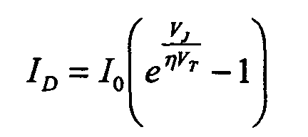 where ID is the biasing current, I 0 is the reverse saturation
current of the junction, VJ is the junction voltage, T is the
junction temperature, VT is the volt equivalent of temperature
at 25°C, and η is a parameter that takes into account the
phenomena of generation and recombination of the charge
carriers within the junction.
where ID is the biasing current, I 0 is the reverse saturation
current of the junction, VJ is the junction voltage, T is the
junction temperature, VT is the volt equivalent of temperature
at 25°C, and η is a parameter that takes into account the
phenomena of generation and recombination of the charge
carriers within the junction.
In particular, Figure 5 shows three curves obtained at three
different junction temperatures, T1, T2 and T3, with T3 < T2 <
T1. As can be seen, if the forward-biasing current IREF is kept
constant, the junction voltage VJ increases as the junction
temperature decreases.
If the bipolar junction 31 is directly biased with a constant
current IREF and the junction voltage VJ is acquired, it is
hence possible to derive the value of the bit stored.
Preferably, the read/write device 20 comprises one or more
dummy elements, which have the same structure as the
read/write elements 3 and can be used as references during
reading so as to prevent undesired changes of temperature
and/or of biasing current from causing data reading errors
(offset compensation). Conveniently, the dummy elements are
not bent and hence do not present the stress region 28 at the
base of the arms 25 and 26. The dummy elements can be used,
for example, in the read circuit 40 shown in Figure 6 and
integrated in the mass storage device 1 of Figure 1.
In detail, the read circuit 40 comprises two current sources
41, which are equal to one another, connected respectively to
a read/write element 3 of the type shown in Figures 2-4 and to
a dummy element, here designated by 42. The current sources 41
supply constant currents IREF and can be obtained via a single
current-mirror circuit (not shown) with two outputs.
The read circuit 40 further comprises an operational amplifier
43, having a non-inverting terminal connected to the
read/write element 3 and an inverting terminal connected to
the dummy element 42; and a comparator stage 44, connected to
the output of the operational amplifier 43 and outputting a
digital voltage VOUT representing the read data bit.
In an alternative embodiment, the concentration of the dopant
atoms is regulated so as to obtain a Zener diode having a
reverse breakdown voltage of approximately 3 V, and writing is
carried out by reverse-biasing of the bipolar junction 31.
Thereby, a considerable decrease of the write current is
obtained. In fact, given the dissipation of power P necessary
for reaching the writing temperature, the current required in
a reverse-biased Zener diode is:
I1 = P/3 V
while the current required in a forward-biased diode with a
junction voltage of 0.7 V is:
I2 = P/0.7 V
hence higher by a factor of four. Thus, if a Zener diode is
used, it is possible to use a simpler driving electronics and
consequently achieve reduced overall dimensions and
consumption levels.
The read/write device described presents the advantages
outlined hereinafter.
First, the detection of temperature is directly linked to the
intrinsic physical properties of semiconductors and hence is
independent of external parameters, such as the geometrical
dimensions of the device.
Reading of the data in the memory is thus much more reliable
and in particular insensitive to any geometrical dimension
spread due to the fabrication process.
Furthermore, temperature detection via a bipolar junction is
affected by lower intrinsic noise as compared to temperature
detection obtained via a resistance variation.
Finally, it is clear that modifications and variations may be
made to the read/write device described and illustrated
herein, without thereby departing from the scope of the
present invention, as defined in the annexed claims.
Claims (13)
- A data-storage device (1) comprising:characterized in that said local probe (6, 31) comprises a bipolar junction (31).a data-storage medium (5), storing data as local deformations (32); andat least one read/write element (3) carrying a local probe (6, 31) facing said data-storage medium (5);
- The data-storage device according to claim 1, wherein said read/write element (3) comprises a supporting structure (25, 26) carrying said local probe (6, 31).
- The data-storage device according to claim 2, comprising a substrate (4) of semiconductor material, and at least one cavity (22) formed within said substrate (4); said supporting structure comprising a first and a second arm (25, 26) of semiconductor material, said first and second arms (25, 26) being carried by said substrate (4), extending in cantilever fashion above said cavity (22), and carrying said bipolar junction (31).
- The data-storage device according to claim 3, wherein said first and second arms (25, 26) are connected to one another at a free end (25b, 26b) and form said bipolar junction (31).
- The data-storage device according to claim 4, wherein said first arm (25) has a first doping type, and said second arm (26) has a second doping type.
- The data-storage device according to any of the preceding claims, wherein said semiconductor material is silicon.
- The data-storage device according to any of the preceding claims, wherein said bipolar junction (31) forms a Zener diode.
- The data-storage device according to any of the preceding claims, wherein said local probe (6, 31) further comprises a tip (6) extending from said bipolar junction (31) and facing said data-storage medium (5), said data-storage medium (5) comprising a layer that can be deformed by said tip (6).
- The data-storage device according to any of the preceding claims, further comprising a reading circuit (40) connected to said read/write element (3) and configured to generate an electrical signal (VOUT) according to the local deformation (32) detected by said local probe (6, 31).
- A method for reading a data-storage device (1) comprising a data-storage medium (5) locally deformable to store a datum; and at least one reading element (3) carrying a local probe (6, 31) facing said data-storage medium (5), the method comprising the step of supplying a first electrical quantity (IREF) to said reading element (3) and detecting a second electrical quantity (VJ ), which is correlated to said first electrical quantity (IREF) and has a value that depends upon the datum stored in said data-storage medium (5); said method being characterized in that it comprises the step of biasing a bipolar junction (31).
- The method according to claim 10, wherein said first electrical quantity is a current (IREF), and said second electrical quantity is a voltage (VJ ).
- The method according to claim 10 or claim 11, wherein said bipolar junction (31) is forward-biased.
- The method according to claim 10 or claim 11, wherein said bipolar junction (31) is reverse-biased.
Priority Applications (2)
| Application Number | Priority Date | Filing Date | Title |
|---|---|---|---|
| EP03425826A EP1550850A1 (en) | 2003-12-29 | 2003-12-29 | Read/Write device for a mass storage device, and Read/Write method thereof |
| US11/019,933 US7885168B2 (en) | 2003-12-29 | 2004-12-21 | Read/write device for a mass storage device, and read/write method thereof |
Applications Claiming Priority (1)
| Application Number | Priority Date | Filing Date | Title |
|---|---|---|---|
| EP03425826A EP1550850A1 (en) | 2003-12-29 | 2003-12-29 | Read/Write device for a mass storage device, and Read/Write method thereof |
Publications (1)
| Publication Number | Publication Date |
|---|---|
| EP1550850A1 true EP1550850A1 (en) | 2005-07-06 |
Family
ID=34560258
Family Applications (1)
| Application Number | Title | Priority Date | Filing Date |
|---|---|---|---|
| EP03425826A Withdrawn EP1550850A1 (en) | 2003-12-29 | 2003-12-29 | Read/Write device for a mass storage device, and Read/Write method thereof |
Country Status (2)
| Country | Link |
|---|---|
| US (1) | US7885168B2 (en) |
| EP (1) | EP1550850A1 (en) |
Cited By (1)
| Publication number | Priority date | Publication date | Assignee | Title |
|---|---|---|---|---|
| US7885168B2 (en) | 2003-12-29 | 2011-02-08 | Stmicroelectronics, S.R.L. | Read/write device for a mass storage device, and read/write method thereof |
Families Citing this family (2)
| Publication number | Priority date | Publication date | Assignee | Title |
|---|---|---|---|---|
| US7173547B2 (en) * | 2004-03-22 | 2007-02-06 | International Business Machines Incorporated | Offset compensation in local-probe data storage devices |
| ITTO20060904A1 (en) * | 2006-12-19 | 2008-06-20 | St Microelectronics Srl | PROCEDURE FOR THE MANUFACTURE OF PROBES INTENDED FOR INTERACTION WITH A STORAGE AND PROBE OBTAINED IN THIS MODE |
Citations (6)
| Publication number | Priority date | Publication date | Assignee | Title |
|---|---|---|---|---|
| US3334352A (en) * | 1965-03-18 | 1967-08-01 | Blh Electronics | Thermal recording |
| US5323377A (en) * | 1992-11-27 | 1994-06-21 | Chen Zhi Q | Electrical data recording and retrieval based on impedance variation |
| US5713667A (en) * | 1995-06-07 | 1998-02-03 | Advanced Micro Devices, Inc. | Temperature sensing probe for microthermometry |
| US5751683A (en) * | 1995-07-24 | 1998-05-12 | General Nanotechnology, L.L.C. | Nanometer scale data storage device and associated positioning system |
| US5886922A (en) * | 1997-05-07 | 1999-03-23 | Hewlett-Packard Company | Probe device for memory device having multiple cantilever probes |
| WO2002037488A1 (en) * | 2000-11-03 | 2002-05-10 | International Business Machines Corporation | Afm-based data storage and microscopy |
Family Cites Families (10)
| Publication number | Priority date | Publication date | Assignee | Title |
|---|---|---|---|---|
| DE69722702T2 (en) * | 1996-04-18 | 2004-04-29 | Seiko Instruments Inc. | Semiconductor strain sensors with pn junction, scanning probe microscope |
| US5835477A (en) | 1996-07-10 | 1998-11-10 | International Business Machines Corporation | Mass-storage applications of local probe arrays |
| JPH11304825A (en) * | 1997-09-30 | 1999-11-05 | Seiko Instruments Inc | Semiconductor strain sensor, method of manufacturing the same, and scanning probe microscope |
| JP3883699B2 (en) * | 1997-11-20 | 2007-02-21 | エスアイアイ・ナノテクノロジー株式会社 | Self-sensing SPM probe and SPM device |
| US6479892B1 (en) * | 2000-10-31 | 2002-11-12 | Motorola, Inc. | Enhanced probe for gathering data from semiconductor devices |
| JP3786608B2 (en) * | 2002-01-28 | 2006-06-14 | 株式会社ルネサステクノロジ | Semiconductor integrated circuit device |
| US7126139B2 (en) * | 2003-10-09 | 2006-10-24 | The Regents Of The University Of California | Device and method of positionally accurate implantation of individual particles in a substrate surface |
| US7423954B2 (en) * | 2003-12-17 | 2008-09-09 | Hewlett-Packard Development Company, L.P. | Contact probe storage sensor pod |
| US7436753B2 (en) * | 2003-12-17 | 2008-10-14 | Mejia Robert G | Contact probe storage FET sensor |
| EP1550850A1 (en) | 2003-12-29 | 2005-07-06 | STMicroelectronics S.r.l. | Read/Write device for a mass storage device, and Read/Write method thereof |
-
2003
- 2003-12-29 EP EP03425826A patent/EP1550850A1/en not_active Withdrawn
-
2004
- 2004-12-21 US US11/019,933 patent/US7885168B2/en not_active Expired - Fee Related
Patent Citations (6)
| Publication number | Priority date | Publication date | Assignee | Title |
|---|---|---|---|---|
| US3334352A (en) * | 1965-03-18 | 1967-08-01 | Blh Electronics | Thermal recording |
| US5323377A (en) * | 1992-11-27 | 1994-06-21 | Chen Zhi Q | Electrical data recording and retrieval based on impedance variation |
| US5713667A (en) * | 1995-06-07 | 1998-02-03 | Advanced Micro Devices, Inc. | Temperature sensing probe for microthermometry |
| US5751683A (en) * | 1995-07-24 | 1998-05-12 | General Nanotechnology, L.L.C. | Nanometer scale data storage device and associated positioning system |
| US5886922A (en) * | 1997-05-07 | 1999-03-23 | Hewlett-Packard Company | Probe device for memory device having multiple cantilever probes |
| WO2002037488A1 (en) * | 2000-11-03 | 2002-05-10 | International Business Machines Corporation | Afm-based data storage and microscopy |
Non-Patent Citations (1)
| Title |
|---|
| VETTIGER P ET AL: "THE MILLIPEDE-NANOTECHNOLOGY ENTERING DATA STORAGE", IEEE TRANSACTIONS ON NANOTECHNOLOGY, IEEE SERVICE CENTER, PISCATAWAY, NY, US, vol. 1, no. 1, March 2002 (2002-03-01), pages 39 - 55, XP001186695, ISSN: 1536-125X * |
Cited By (1)
| Publication number | Priority date | Publication date | Assignee | Title |
|---|---|---|---|---|
| US7885168B2 (en) | 2003-12-29 | 2011-02-08 | Stmicroelectronics, S.R.L. | Read/write device for a mass storage device, and read/write method thereof |
Also Published As
| Publication number | Publication date |
|---|---|
| US7885168B2 (en) | 2011-02-08 |
| US20050162932A1 (en) | 2005-07-28 |
Similar Documents
| Publication | Publication Date | Title |
|---|---|---|
| US7482826B2 (en) | Probe for scanning over a substrate and a data storage device | |
| JP5313522B2 (en) | Multi-level data storage device with phase change material | |
| US7042828B2 (en) | Nanometer scale data storage device and associated positioning system | |
| US5856672A (en) | Single-crystal silicon cantilever with integral in-plane tip for use in atomic force microscope system | |
| US7697403B2 (en) | Data read/write systems comprising a tip | |
| US5729026A (en) | Atomic force microscope system with angled cantilever having integral in-plane tip | |
| KR100746768B1 (en) | Information recording and reading device using cantilever | |
| US7885168B2 (en) | Read/write device for a mass storage device, and read/write method thereof | |
| US7355955B2 (en) | Nanoscale digital data storage device | |
| JP4979229B2 (en) | Probe that scans across the substrate | |
| KR100558376B1 (en) | MOSFF cantilever for atomic force microscopy | |
| US8373431B2 (en) | Probe for scanning over a substrate and data storage device | |
| US20030202456A1 (en) | Apparatus and method for reproducing data using capacitance variation | |
| CN100578631C (en) | Data recording system and method of using the same | |
| US20060212978A1 (en) | Apparatus and method for reading bit values using microprobe on a cantilever | |
| KR100519221B1 (en) | Cantilever of variable conductivity type and manufacturing method thereof, for use in nano data storage device | |
| KR100634552B1 (en) | Field sensing probe with separated sensor and information storage device with same | |
| KR100682921B1 (en) | Semiconductor probe with piezoresistive sensor with vertical PUN junction structure | |
| US20110058465A1 (en) | Microelectromechanical device having an electromagnetic micromotor, in particular mass storage device made by probe storage technology | |
| KR100585670B1 (en) | Probe type data storage with adjustable gap between tip and media | |
| KR20040031534A (en) | Method of manufacturing cantilever for data storage device |
Legal Events
| Date | Code | Title | Description |
|---|---|---|---|
| PUAI | Public reference made under article 153(3) epc to a published international application that has entered the european phase |
Free format text: ORIGINAL CODE: 0009012 |
|
| AK | Designated contracting states |
Kind code of ref document: A1 Designated state(s): AT BE BG CH CY CZ DE DK EE ES FI FR GB GR HU IE IT LI LU MC NL PT RO SE SI SK TR |
|
| AX | Request for extension of the european patent |
Extension state: AL LT LV MK |
|
| 17P | Request for examination filed |
Effective date: 20060104 |
|
| AKX | Designation fees paid |
Designated state(s): DE FR GB IT |
|
| 17Q | First examination report despatched |
Effective date: 20070829 |
|
| STAA | Information on the status of an ep patent application or granted ep patent |
Free format text: STATUS: THE APPLICATION IS DEEMED TO BE WITHDRAWN |
|
| 18D | Application deemed to be withdrawn |
Effective date: 20080109 |